

Ene KB3700 Schematics

Headquarters
ENE RESERVES THE RIGHT TO AMEND THIS DOCUMENT WITHOUT NOTICE AT ANY TIME. ENE ASSUMES
NO RESPONSIBILITY FOR ANY ERRORS APPEAR IN THE DOCUMENT, AND ENE DISCLAIMS ANY EXPRESS
NG LIABILITY OR
WARRANTIES RELATING TO FITNESS FOR A PARTICULAR PURPOSE, OR INFRINGEMENT OF ANY
Taipei Office
KB3700
Keyboard Controller
Datasheet
Revision 0.1
July. 2006
OR IMPLIED WARRANTY, RELATING TO SALE AND/OR USE OF ENE PRODUCTS INCLUDI
PATENTS, COPYRIGHTS OR OTHER INTELLECTUAL PROPERTY RIGHTS.
Copyright©2006, ENE Technology Inc. All rights reserved.
4F-1, No.9, Prosperity Rd.,
Science-based Industrial Park,
Hsinchu City, Taiwan, R.O.C
TEL: 886-3-6662888
FAX: 886-3-6662999
http://www.ene.com.tw
9F, No.88, Bauchiau Rd.
Shindian City, Taipei,
Taiwan, R.O.C.
TEL: 886-2-89111525
FAX: 886-2-89111523

C
ONTENT
KB3700 Keyboard Controller Datasheet
1. FEATURES................................................................................................................... 4
1.1 F
EATURE SUMMARY
1.2 B
LOCK DIAGRAM
................................................................................................................ 4
.................................................................................................................... 7
2. PIN ASSIGNMENT AND DESCRIPTION...............................................................8
2.1 P
IN LIST
2.2 I/O B
2.3 I/O B
2.4 I/O N
................................................................................................................................. 8
UFFER TABLE
UFFER CHARACTERISTIC TABLE
AMING CONVENTION
................................................................................................................. 9
......................................................................................9
....................................................................................................... 9
3. PIN DESCRIPTIONS................................................................................................ 10
3.1 H
ARDWARE TRAP
.................................................................................................................. 10
4. MODULE DESCRIPTIONS..................................................................................... 10
4.1 C
HIP ARCHITECTURE
4.1.1 Power Planes ....................................................................................................................11
4.1.2 Clock Domains..................................................................................................................11
4.1.3 Reset Domains ..................................................................................................................11
4.2 GPIO....................................................................................................................................11
4.2.1 GPIO Functional Description...........................................................................................11
4.2.2 GPIO Input / Output Control Structure............................................................................ 13
4.3 KBC.................................................................................................................................... 14
4.3.1 KBC Functional Description ........................................................................................... 14
4.3.2 KBC Registers Descriptions (Base Address = FC80h, 32 bytes)..................................... 15
4.4 PWM................................................................................................................................... 15
4.4.1 PWM Functional Description.......................................................................................... 16
4.4.2 PWM Registers Descriptions (Base address_FE00h, 16 bytes)....................................... 16
4.5 GPT .................................................................................................................................... 17
4.5.1 GPT Functional Description............................................................................................ 17
4.5.2 GPT Register Descriptions (Base address = FE50h, 16 bytes) ....................................... 17
4.6 SPI/ISP D
EVICE INTERFACE
.............................................................................................................11
.................................................................................................. 18
4.6.1 SPI/ISP Functional Description....................................................................................... 18
4.6.2 SPI Registers Descriptions (Base address = FE70h, 16 bytes) ....................................... 18
4.6.3 ISP Registers Descriptions (8 bytes)................................................................................ 19
4.7 WDT....................................................................................................................................21
4.7.1 WDT Functional Description........................................................................................... 21
4.7.2 WDT Registers Descriptions (Base address = FE80h, 16 bytes)..................................... 21
Copyright©2006, ENE Technology Inc. 2

4.8 LPC.....................................................................................................................................22
4.8.1 LPC / FWH Functional Description ................................................................................ 22
4.8.1.1 LPC Decoding IO Ports................................................................................................ 22
4.8.1.2 LPC Decoding Memory Space...................................................................................... 22
4.8.2 LPC Registers Descriptions (Base address = FE90h, 16 bytes)...................................... 22
4.9 PS / 2 I
4.10 EC..................................................................................................................................... 26
4.10.1.1 Hardware EC Commands ................................................................................................................ 26
4.10.1.2 EC Status Register.............................................................................................................................26
4.10.1.3 EC Command Register.....................................................................................................................26
4.10.1.4 EC Command Program Sequence ...................................................................................................27
4.10.1.5 EC Index IO Mode............................................................................................................................27
NTERFACE
4.9.1 PS/2 Functional Description............................................................................................ 24
4.9.2 PS2 Registers Descriptions (Base Address = FEE0h, 32 bytes)...................................... 24
4.10.1 EC Functional Description ............................................................................................ 26
................................................................................................................. 24
KB3700 Keyboard Controller Datasheet
4.10.1.6 SCI Generation.................................................................................................................................. 27
4.10.1.7 SCI ID Table ...................................................................................................................................... 28
4.10.2 EC Register Descriptions (Base Address = FF00h, 32 bytes) ....................................... 28
4.11 GPWU............................................................................................................................... 32
4.11.1 GPWU Functional Description...................................................................................... 32
4.11.2 GPWU Register Descriptions (Base Address = FF30h, 96 bytes)................................. 32
4.12 8051 M
ICROPROCESSOR
4.12.1 Interrupt Vectors Table................................................................................................... 32
4.12.2 SFR Map ........................................................................................................................ 33
4.12.3 SFR Descriptions ........................................................................................................... 34
.................................................................................................... 32
5. ELECTRONIC CHARACTERISTICS ...................................................................37
5.1 A
BSOLUTE MAXIMUM RATING
5.2 R
ECOMMENDED OPERATING CONDITION
5.3 O
PERATING CURRENT
........................................................................................................... 37
................................................................................................ 37
................................................................................37
6. PACKAGING INFORMATION............................................................................... 39
6.1 64 LQFP ............................................................................................................................. 39
7. REVISION HISTORY............................................................................................... 40
Copyright©2006, ENE Technology Inc. 3

1. Features
1.1 Feature Summary
Low Pin Count Host Interface (LPC)
SIRQ supporting IRQ1, IRQ12, SCI
I/O Address Decoding:
KBC IO Port 60h/64h
Programmable EC IO Port 62h/66h and 68h/6Ch
Programmable 4-byte Index I/O ports to access internal registers
One Programmable I/O write byte-address decoding
X-Bus Interface (XBI)
SPI Flash support, the operation frequency runs at least 50MHz.
Addressable Memory range up to 24MB.
8051 64KB code memory can be mapped into 4 independent 16KB pages.
KB3700 Keyboard Controller Datasheet
8051 Microprocessor
Industry 8051 Instruction set complaint with 3~5 cycles per instruction.
Programmable 8/16/32 MHz clock
Fast instruction fetching from XBI Interface
128 bytes and 2KB tightly-coupled SRAM
24 extended interrupt sources.
Two 16-bit tightly-coupled timer
8042 Keyboard Controller
8 Standard keyboard commands processed by hardware
Each hardware command can be optionally processed by firmware
Embedded Controller (EC)
Five EC Standard Commands can be processed by hardware
ACPI Specification 2.0 compliant
Support customer command by firmware
Programmable EC I/O port addressing (default 62h/66h)
Analog To Digital Converter (ADC)
6 built-in ADCs with 8-bit resolution.
The ADC pins can be alternatively configured as General Purpose Inputs (GPI).
Copyright©2006, ENE Technology Inc. 4

KB3700 Keyboard Controller Datasheet
Pulse Width Modulator (PWM)
5 built-in PWMs
Selectable clock sources: 1MHz/64KHz/4KHz/256Hz.
Configurable cycle time (up to 1 sec) and duty cycle.
Watchdog Timer (WDT)
32.768KHz input clock with 20-bit time scale.
8-bit watchdog timer interrupt and reset setting
General Purpose Timer (GPT)
Two 16-bit, two 8-bit general purpose timers with 32.768KHz resolution
General Purpose Wake-Up (GPWU)
All General Purpose Input pins can be configured to generate interrupts or
wake-up event.
General Purpose Input/Output (GPIO)
All I/O pins are bi-direction and configurable
All outputs can be optionally tri-stated
All inputs equipped with pull-up, high/low active, edge/level trigger selection
All GPIO pins are bi-direction, input and output.
Max. 43 GPIOs
Power Management
Sleep State: 8051 Program Counter (PC) stopped
Deep Sleep State: Stop all internal clocks. Target power consumption ~10uA.
Copyright©2006, ENE Technology Inc. 5
KB3700 64-pin LQFP KB3920 144-pin LQFP
Chip Dimension
Microprocessor
Built-in SRAM
8051 Clock
Flash Memory Range
Flash I/F Clock
ADC
DAC
Watch Dog Timer
PWM
External PS/2 devices
GPIOs
KB matrix scan
FAN Controller
General Purpose Timer
SM Bus
HW KBC Standard Commands
HW IKB Standard Commands
HW EC Standard Commands
Power Consumption
KB3700 Keyboard Controller Datasheet
10x10 mm
2
20x20 mm
2
8051 8051
2048 + 128 bytes 2048 + 128 bytes
32 ~8 MHz (adjustable) 22~8 MHz
4M bytes (SPI) 1M bytes(ISA), 2M bytes (SPI)
65~32 MHz (adjustable) 65/32 MHz (2 select 1)
6 4
N.A. 4
1 1
5 4
2 3
Max 43 Max 89 pins
N.A. 18x8
N.A. 2
6 6
N.A. 2 Interfaces
N.A. 1 Internal Controller
8 8
N.A. 10
5 5
TBD (target 12mA) 15 mA(in Normal RUN)
TBD (target 3mA in IDLE mode) 4 mA (in IDLE mode)
TBD
(target 500 uA in STOP mode)
10 uA( in STOP mode)
Copyright©2006, ENE Technology Inc. 6
1.2 Block Diagram
KB3700 Keyboard Controller Datasheet
Copyright©2006, ENE Technology Inc. 7
KB3700 Keyboard Controller Datasheet
2. Pin Assignment and Description
2.1 Pin List
No. Pin Name GPIO Alt. Output. Alt. Input Default Reset IOCELL
1 GPIOE0 GPIOE0 BQC04HU
2 GPIOE1 GPIOE1 BQC04HU
3 GPIOE2 GPIOE2 BQC04HU
4 GPIOE3 GPIOE3 BQC04HU
5 SERIRQ BCC16H
6 GPIO00 GPIO00 GA20 BQC04HU
7 LFRAME#
8 LAD3 BCC16H
9 GPIO01 GPIO01 KBRST# BQC04HU
10 GPIO02 GPIO02 PLLCLK_REF2 BQC04HU
11 LAD2 BCC16H
12 LAD1 BCC16H
13 VCC VCC
14 LAD0 BCC16H
15 GND GND
16 GPIO03 GPIO03 PCICLK BCC16H
17 GPIOE4 GPIOE4 BQC04HU
18 GPIOE5 GPIOE5 BQC04HU
19 GPIOE6 GPIOE6 BQC04HU
20 GPIOE7 GPIOE7 BQC04HU
21 GPIO04 GPIO04 PCIRST# BCC16H
22 GPIO05 GPIO05 SCI# BQC04HU
23 GPIO06 GPIO06 PWM0/E51_TXD BCC16H
24 GPIO07 GPIO07 PWM1/E51_CLK E51_RXD BCC16H
25 GPIO08 GPIO08 PWM2 BCC16H
26 GPIO09 GPIO09 PWM3 BCC16H
27 GPIO0A GPIO0A PWM4 BCC16H
28 GPIO0B GPIO0B E51_TMR0 BQC04HU
29 GPIO0C GPIO0C E51_TMR1 BQC04HU
30 GPIO0D GPIO0D E51_TXD ECRST# BQC04HU
31 GPIO0E GPIO0E PLLCLK32 E51_INT0 ECRST# BQC04HU
32 GPIO0F GPIO0F POR E51_INT1 BQC04HU
33 GPIOE8 GPIOE8 BQC04HU
34 AD3 IQA
35 AD4 IQA
36 AD5 IQA
37 GPIO10 GPIO10 BQC04HU
38 AD0 IQA
39 AD1 IQA
40 AD2 IQA
41 AVCC AVCC
42 AGND AGND
43 GPIO11 GPIO11 PSCLK1 PSCLK1 BQC04HU_10K
44 GPIO12 GPIO12 PSDAT1 PSDAT1 BQC04HU_10K
BCC16H
Copyright©2006, ENE Technology Inc. 8
45 GPIO13 GPIO13 PSCLK2 PSCLK2 BQC04HU_10K
46 GPIO14 GPIO14 PSDAT2 PSDAT2 BQC04HU_10K
47 GPIO15 GPIO15 TEST_CLK BQC04HU
48 GPIO16 GPIO16 TP_CLK_TEST BQC04HU
49 GPIOEC GPIOEC BQC04HU
50 GPIOED GPIOED BQC04HU
51 GPIOEE GPIOEE BQC04HU
52 GPIOEF GPIOEF BQC04HU
53 GPIO17 GPIO17 CLK TP_PLL_TEST BQC04HU
54 GPIO18 GPIO18 CLK32MHz(8051) TP_ISP_MODE BQC04HU
55 GPIO19 GPIO19 CLK16MHz(peri) TP_IO_TEST BQC04HU
56 GPIO1A GPIO1A CLK32MHz(WDT BQC04HU
57 GPIO1B GPIO1B BQC04HU
58 SPIDI BCC16H
59 SPIDO BCC16H
60 SPICLK BCC16H
61 SPICS# BCC16H
62 VCC VCC
63 VCC18 VCC18
64 GND GND
KB3700 Keyboard Controller Datasheet
2.2 I/O Buffer Table
IO Name Descriptions Applications
BQC04HU Schmitt trigger, 2~4mA Output / Sink Current, with , Input / Output / Pull Up Enable GPIO
BQC04HU_10K Schmitt trigger, 2~4mA Output / Sink Current, with , Input / Output / 10KΩ Pull Up Enable GPIO
BCC16H 8~16mA Output / Sink Current , 5 V Tolerance, Input / Output Enable LPC Interface
IQA Mixed mode IO, ADC Enable, with GPI, 2~4mA Sink Current, Input Enable ADC, GPIN
2.3 I/O Buffer Characteristic Table
IO Name
Port
BQC04HU V V V V V 40K (typ.)
BQC04HU_10K
BCC16H V V V V V V 8~16mA
IQA V V V V
IO I O OE IE AE 5VTor PE
V V V V V 10K (typ.)
Output / Sink
Current
2~4mA
2~4mA
2.4 I/O Naming Convention
I IO Buffer Input
O IO Buffer Output
OE IO Buffer Output Enable
IE IO Buffer Input Enable
PE IO Buffer Pull High Enable
AE IO Buffer Analog mode Enable(AE > OE)
Q Schmitt Trigger
H 5V Tolerance
Copyright©2006, ENE Technology Inc. 9
1
2
3
4
5
6
7
8
9
10
11
Embedded Controller
(hardware EC Space)
12
General Purpose Wake
-
up
(hardware EC Space)
KB3700 Keyboard Controller Datasheet
3. Pin Descriptions
3.1 Hardware trap
Hardware trap pins will latch the external signal levels at the rising edge of ECRST#. Either a High
or Low value will be stored internally to serve as control signals as described below.
For normal application, there is no application component required for selecting the normal mode
because KB3700 build-in internal pull up resistor to select the right operation mode.
After KB3700 booted, the pull up resistor may be disabled by GPIO register setting.
Pin name 64 Pins
TP_TEST
48
(GPIO16)
TP_PLL
53
(GPIO17)
TP_TEST: Clock Test Mode (for testing and ISP Mode)
Low: Clock Test Mode Enable. (all internal logic will use GPIO15 as clock
source)
TP_PLL: PLL Test Mode (for testing)
LOW: PLL Test Mode Enable
GPIO0E is PLL 32MHz clock output.
GPIO0F is Power On Reset output.
HW Strap Description
HIGH: Normal operation (MUST, Power-On Default)
TP_ISP
54
(GPIO18)
TP_IO
55
(GPIO19)
TP_ISP: ISP Mode (for programming external SPI flash)
LOW: ISP Mode Enable
HIGH: Normal operation in not ISP mode (MUST, Power-On Default)
TP_IO: IO Test Mode (for testing)
LOW: IO Test Mode Enable
HIGH: Normal operation (MUST, Power-On Default)
4. Module Descriptions
The following table gives the corresponding memory map for accessing. Each module will be
described detail in the individual sections.
No. Abbreviation
Flash Program space mapped to system BIOS 0000h~F3FFh 61K
XRAM Embedded SRAM F400h~FBFFh 2K
GPIO General Purpose IO (include ADC, DAC) FC00h~FC7Fh 128
KBC Keyboard Controller FC80h~FC9Fh 32
PWM Pulse Width Modulation FE00h~FE1Fh 32
GPT General Purpose 16-bit timer FE50h~FE6Fh 32
WDT Watchdog Timer FE80h~FE8Fh 16
LPC Low Pin Count FE90h~FE9Fh 16
XBI X-BUS Interface FEA0h~FECFh 48
PS2 PS2 FEE0h~FEFFh 32
EC
GPWU
Device Full Name Address Range Size (Byte)
FF00h~FF1Fh 32
FF20h~FE7Fh 96
1K
Copyright©2006, ENE Technology Inc. 10
GPIOD00
4.1 Chip Architecture
4.1.1 Power Planes
There are 2 power planes in this chip. One is used for all logic, the other is used for Analog
parts (ADC).
4.1.2 Clock Domains
There are 4 clock domain in KB3700.
Flash chip interface clock. The clock default in 16MHz, and can be to 32MHz or 64MHz.
8051 / XBI use high clock (setting in CLKCFG, FF0Dh), ranges from 22~4MHz.
WDT uses 32.768KHz clock. WDT default use internal 32KHz clock. The WDTCFG bit 7
options can switch WDT clock to external 32KHz clock oscillator.
Other peripherals (GPWU, PWM,.) use low clock (setting in CLKCFG, FF0Dh), ranges
from 8~2MHz.
4.1.3 Reset Domains
KB3700 Keyboard Controller Datasheet
This chip builds in power on reset. There is also a input reset signal (ECRST#) for global reset.
WDT reset can reset almost all logic, except WDT and GPIO modules. The WDT reset can be
set to only reset 8051 by EC register (PXCFG, FF14h).
There is additional 8051 reset source from EC register (PXCFG, FF14h).
4.2 GPIO
4.2.1 GPIO Functional Description
Multi-function pin Output Function Selection (FS) bit = 0, is set for GPIO Output Function,
and FS bit = 1, is set for Alternative Output. The alternative input function is enabled by Input
Enable register (IE), and is not affected by FS register.
Offset
00
~
03
10
~
15
20
~
Register
Abbreviation
GPIOFS00
GPIOFS08
GPIOFS10
GPIOFS18
GPIOOE00
GPIOOE08
GPIOOE10
GPIOOE18
GPIOEOE0
GPIOEOE8
GPIOD08
Register Full Name
Bit Attr Description
GPIO 00~1B Output Function Selection (0: GPO, 1: Alternative Output)
00h: GPIOFS00 for GPIO00~07 0
7~0 R/W
GPIO 00~1B Output Enable (0: Output Disable, 1: Output Enable)
7~0 R/W
GPIO 00~1B Data Output
7~0
R/W
01h: GPIOFS08 for GPIO08~0F 0
02h: GPIOFS10 for GPIO10~17 0
03h: GPIOFS18 for GPIO18~1B 0
10h: GPIOOE00 for GPIO00~07 0
11h: GPIOOE08 for GPIO08~0F 0
12h: GPIOOE10 for GPIO10~17 0
13h: GPIOOE18 for GPIO18~1B 0
14h: GPIOEOE0 for GPIOE0~7 0
15h: GPIOEOE8 for GPIOE8~F (GPIOE9~A is N.A.) 0
20h: GPIOD00 for GPIO00~07 0
Def Bnk
FC
FC
FC
Copyright©2006, ENE Technology Inc. 11

30
~
36
40
~
45
50
~
53
60
~
66
GPIOIN00
GPIOIN08
GPIOIN10
GPIOIN18
GPIOEIN0
GPIOEIN8
GPIADIN
GPIOPU00
GPIOPU08
GPIOPU10
GPIOPU18
GPIOEPU0
GPIOEPU8
GPIOOD00
GPIOOD08
GPIOOD10
GPIOOD18
GPIOIE00
GPIOIE08
GPIOIE10
GPIOIE18
GPIADIE
KB3700 Keyboard Controller Datasheet
21h: GPIOD08 for GPIO08~0F 0
22h: GPIOD10 for GPIO10~17 0
23h: GPIOD18 for GPIO18~1B 0
24h: GPIOED0 for GPIOE0~7 0
25h: GPIOED8 for GPIOE8~F (GPIOE9~A is N.A.) 0
GPIO 00~1B Input Status
30h: GPIOIN00 for GPIO00~07
31h: GPIOIN08 for GPIO08~0F
32h: GPIOIN10 for GPIO10~17
7~0 R/W
GPIO 00~1B Pull Up Enable
R/WC
7~0
1
GPIO 00~1B Open Drain Enable
7~0 R/W
GPIO 00~1B Input Enable
7~0 R/W
GPIO MISC
33h: GPIOIN18 for GPIO18~1B
34h: GPIOEIN0 for GPIOEIN0~7
35h: GPIOEIN8 for GPIOEIN8~F (GPIOEIN9~A is N.A.)
36h: GPIAD0 for GPIAD0~5
40h: GPIOPU00 for GPIO00~07 0
41h: GPIOPU08 for GPIO08~0F 20
42h: GPIOPU10 for GPIO10~17 E0
43h: GPIOPU18 for GPIO18~1B 03
44h: GPIOEPU0 for GPIOE0~7 0
45h: GPIOEPU8 for GPIOE8~F (GPIOE9~A is N.A.) 0
50h: GPIOOD00 for GPIO00~07 0
51h: GPIOOD08 for GPIO08~0F 0
52h: GPIOOD10 for GPIO10~17 0
53h: GPIOOD18 for GPIO18~1F 0
60h: GPIOIE00 for GPIO00~07 0
61h: GPIOIE08 for GPIO08~0F 20
62h: GPIOIE10 for GPIO10~17 E0
63h: GPIOIE18 for GPIO18~1B 03
64h: GPIOEIN0 for GPIOE0~7 0
65h: GPIOEIN8 for GPIOE8~F (GPIOE9~A is N.A.) 0
66h: GPIAD0 for GPIAD0~5 0
FC
0
FC
FC
FC
70 GPIOMISC
7~2 RSV 0
FC
1 R/W Select GPIO07 as E51_CLK. 0
0 R/W Select GPIO06 as E51_TXD. 0
Copyright©2006, ENE Technology Inc. 12
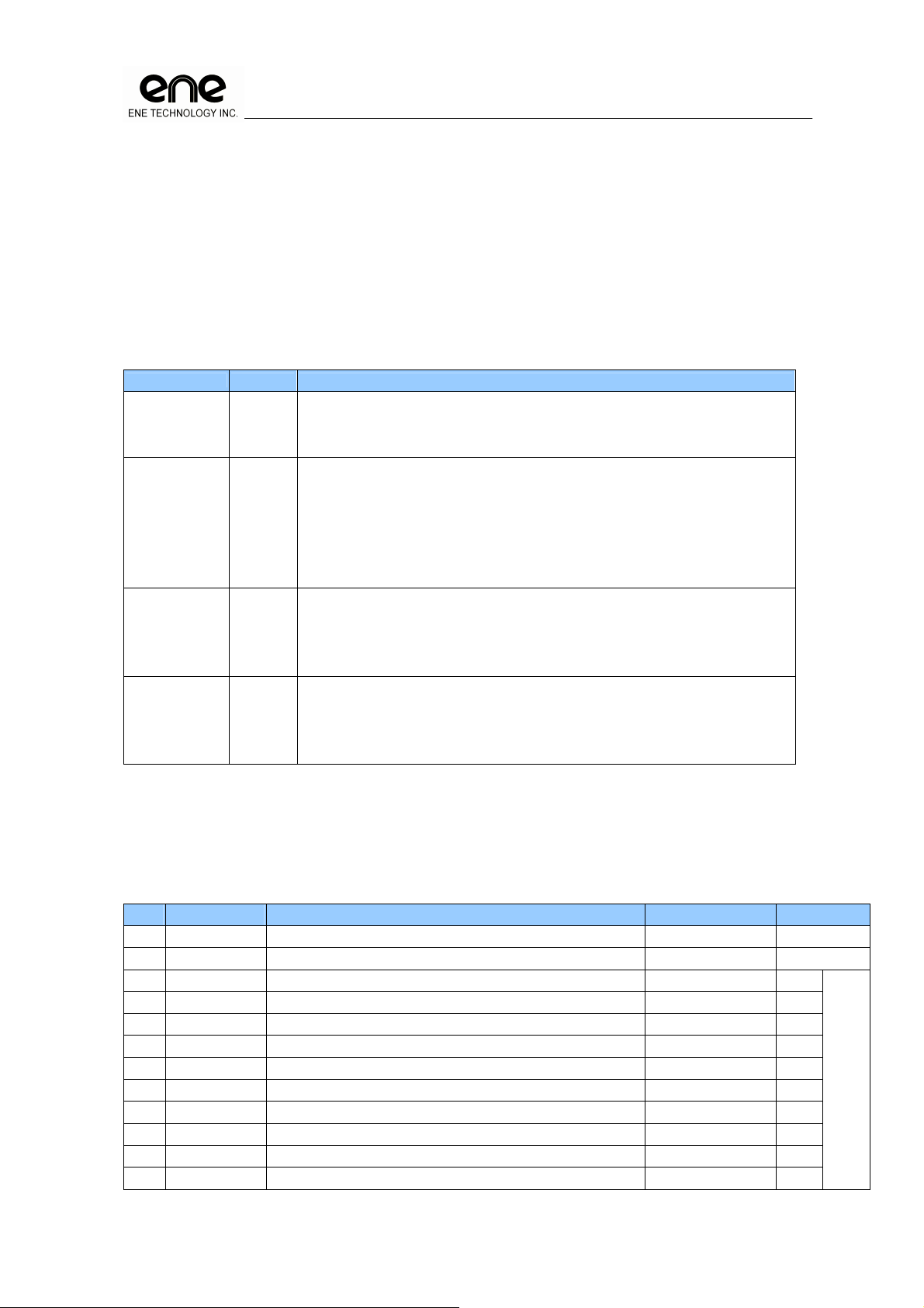
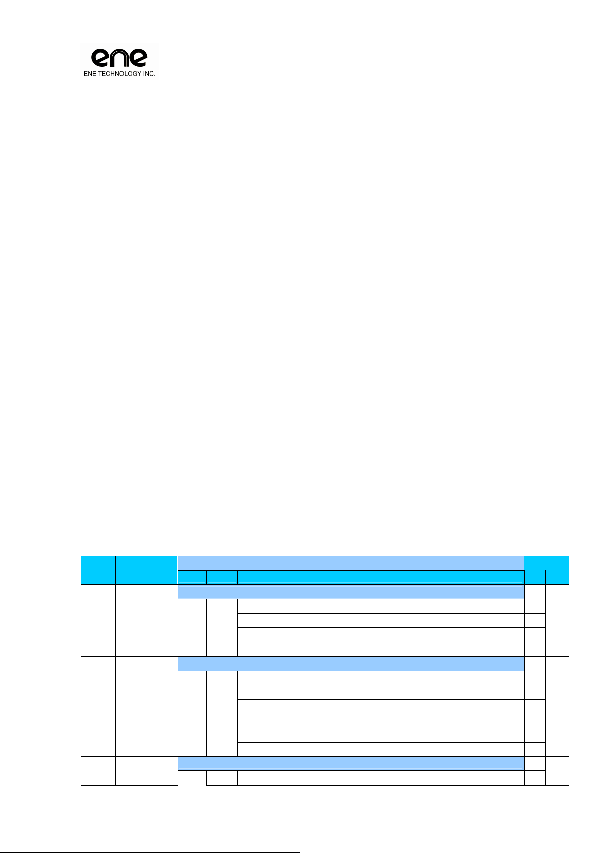
4.2.2 GPIO Input / Output Control Structure
GPIOFS
Alt. Output Enable
GPIOOD
GPIOD
Alt. Output
GPIOFS
GPIOOE
0
1
Pull up Enable
GPIOPIN
Alt Input
0
1
IE
1
0
Output Buffer
Input Buffer
IE
KB3700 Keyboard Controller Datasheet
OE
IO PIN
PE
PE
GPIOPIN
Alt Input
IE
Input Buffer
INPUT PIN
GPIOFS
Alt. Output Enable
GPIOOD
GPIOOE
0
1
1
0
GPIOD
Alt. Output
0
1
GPIOFS
Copyright©2006, ENE Technology Inc. 13
OE
OUTPUT PIN
Output Buffer
 Loading...