EMP EMD2050 Schematic [ru]

ESMT/EMP
EMD2050
PWM Step-Up DC/DC Converter for Panel Backlight
General Description
The EMD2050 designed with high efficiency step up
DC/DC converter for driving white LEDs. The device
can drive up 3 white LEDs from a single Li-Ion battery
or a DC power 2.5V to 5.5V. The EMD2050 uses
current mode and pulse-width modulated (PWM)
operation. It switches at 1.2MHz and allows using
small inductor and both of input/output capacitors.
An internal compensation can reduce external
component.
The EMD2050 include under-voltage lockout, current
limit, over voltage and thermal shutdown protection.
The EMD2050 is available in SOT-26 package.
Applications
Mobile Phone
Digital Still Cameras
Portable applications
MP3 Players
GPS Receivers
Features
WLEDs supports (20mA for each channel):
Up to 3S13P at VIN=3.7V
Up to 3S18P at VIN=5.0V
(Note: SÆ Series; PÆ Parallel)
Low Quiescent Current: 55 μA
Over Voltage Protection: 15V
Inherently Matched LED Current
Shutdown Current < 1μA
Reference Voltage 0.235V
Efficiency : 85% (Typ) at VIN=5.0V
PWM Dimming Control
Internal Soft Start and Compensation
Low Profile SOT-26 Package
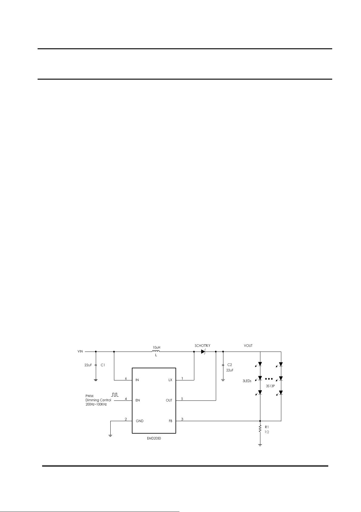
Typical Application (3S13P)
Fig.1
Elite Semiconductor Memory Technology Inc. /Elite MicroPower Inc. Publication Date: Oct. 2009
Revision: 1.0 1/12

ESMT/EMP
EMD2050
Connection Diagram
Order Information
IN
LX GND FB
OUT
65 4
1 32
55
SOT-26
EN
EMD2050-00VC06NRR
00 Output voltage
VC06 SOT-26 Package
NRR RoHS & Halogen free package
Rating: -40 to 85°C
GRR RoHS Package (By Request)
Package in Tape & Reel
Order, Mark & Packing Information
Package Vout Product ID Marking Packing
OUT
SOT-26 Adjustable EMD2050-00VC06NRR
PIN1 DOT
IN
65 4
Tracking Code
1 32
LX GND FB
55
2050
EN
Tape & Reel
3Kpcs
Pin Functions
Pin Name
LX 1
GND 2 Ground Pin.
FB 3
EN 4
OUT 5 Over Voltage Protection Pin.
IN 6 Input Voltage Pin.
SOT-26
Pin #
Switch Pin.
Connect inductor/diode here.
Feedback Pin.
Reference voltage is 0.235V, connect cathode of lowest LED
and resistor here.
Chip Enable Pin.
Connect to 1.2V or higher to enable device, 0.4V or less to
disable device.
Function
Elite Semiconductor Memory Technology Inc. /Elite MicroPower Inc. Publication Date: Oct. 2009
Revision: 1.0 2/12

ESMT/EMP
EMD2050
Absolute Maximum Ratings
Devices are subjected to failure if they stay above absolute maximum ratings
Input Voltage – 0.3V to 6V
EN, VFB Voltages – 0.3V to VIN
LX ,OUT Voltage – 0.3V to 16V
ESD Susceptibility HBM 2kV
MM 200V
Operating Temperature Range –40°C to 85°C
Storage Temperature –65°C to 150°C
Junction Temperature 150°C
Lead Temperature (Soldering, 10 sec) 260°C
Electrical Characteristics
(VCC = 3.7V, TA = 25°C, unless otherwise specified.)
PARAMETER TEST CONDITION MIN TYP MAX UNIT
Under Voltage Lock Out 1.8 2.4 V
Supply Current Continuously Switching 1 mA
Quiescent Current No Switching, VFB = 1V
Shutdown Current VEN < 0.4V 1 uA
Operation Frequency 0.9 1.2 1.5 MHz
Maximum Duty Cycle 93 95 %
Feedback Voltage 0.2115 0.235 0.2585 V
Thermal Shutdown Protection 160
Thermal Shutdown Hysteresis 20
Ron Isw = 200mA 0.5 0.8 ohm
Current Limit 1.4 A
Shutdown Voltage Low 0.4 V
Enable Voltage High 1.2 V
EN Leakage Current 1.3 μA
OVP 15 V
OVP Hysteresis 0.2 1 3 V
47 55 70 μA
℃
℃
Elite Semiconductor Memory Technology Inc. /Elite MicroPower Inc. Publication Date: Oct. 2009
Revision: 1.0 3/12

ESMT/EMP
EMD2050
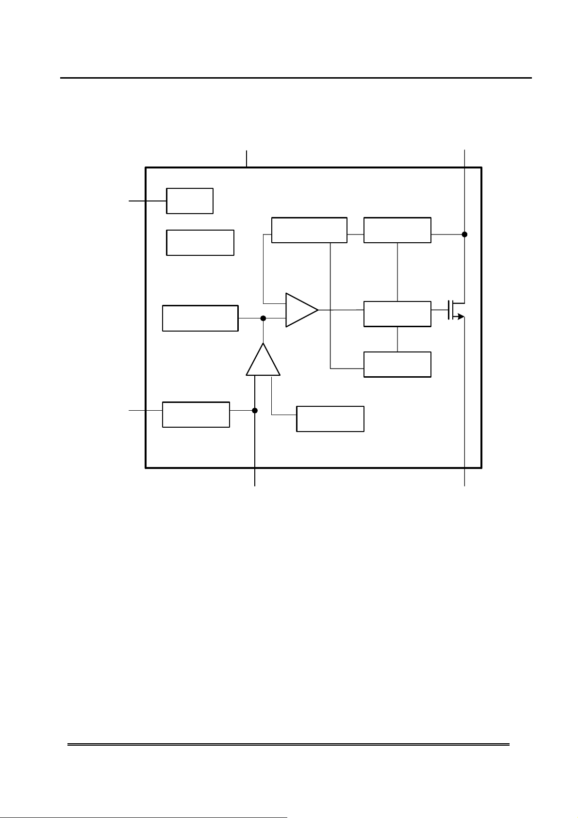
Function block
EN
OUT
EN
UVLO / OTP
INTERNAL
COMPENSATION
OVP
IN
_
+
SLOPE
COMPENSATION
_
+
VERF
LX
CURRENT
SENSER
LOGIC
BUFFER
OSC
GNDFB
Fig.2
Elite Semiconductor Memory Technology Inc. /Elite MicroPower Inc. Publication Date: Oct. 2009
Revision: 1.0 4/12
 Loading...