

Page 1
SERVICE MANUAL
9″ COLOR TV/DVD
EWC09D5 B
Page 2

IMPORTANT SAFETY NOTICE
Proper service and repair is important to the safe, reliable operation of all
Funai Equipment. The service procedures recommended by Funai and
described in this service manual are effective methods of performing
service operations. Some of these service special tools should be used
when and as recommended.
It is important to note that this service manual contains various CAUTIONS
and NOTICES which should be carefully read in order to minimize the risk
of personal injury to service personnel. The possibility exists that improper
service methods may damage the equipment. It also is important to
understand that these CAUTIONS and NOTICES ARE NOT EXHAUSTIVE.
Funai could not possibly know, evaluate and advice the service trade of all
conceivable ways in which service might be done or of the possible
hazardous consequences of each way. Consequently, Funai has not
undertaken any such broad evaluation. Accordingly, a servicer who uses a
service procedure or tool which is not recommended by Funai must first
use all precautions thoroughly so that neither his safety nor the safe
operation of the equipment will be jeopardized by the service method
selected.
Manufactured under license from Dolby Laboratories.
“Dolby” and the double-D symbol are trademarks of Dolby Laboratories.
Page 3

TABLE OF CONTENTS
Specifications . . . . . . . . . . . . . . . . . . . . . . . . . . . . . . . . . . . . . . . . . . . . . . . . . . . . . . . . . . . . . . . . . . . . . . . . . . 1-1-1
Laser Beam Safety Precautions . . . . . . . . . . . . . . . . . . . . . . . . . . . . . . . . . . . . . . . . . . . . . . . . . . . . . . . . . . . . 1-2-1
Important Safety Precautions . . . . . . . . . . . . . . . . . . . . . . . . . . . . . . . . . . . . . . . . . . . . . . . . . . . . . . . . . . . . . . 1-3-1
Standard Notes for Servicing . . . . . . . . . . . . . . . . . . . . . . . . . . . . . . . . . . . . . . . . . . . . . . . . . . . . . . . . . . . . . . 1-4-1
Cabinet Disassembly Instructions. . . . . . . . . . . . . . . . . . . . . . . . . . . . . . . . . . . . . . . . . . . . . . . . . . . . . . . . . . .1-5-1
Electrical Adjustment Instructions . . . . . . . . . . . . . . . . . . . . . . . . . . . . . . . . . . . . . . . . . . . . . . . . . . . . . . . . . . . 1-6-1
How to Initialize the TV/DVD. . . . . . . . . . . . . . . . . . . . . . . . . . . . . . . . . . . . . . . . . . . . . . . . . . . . . . . . . . . . . . . 1-7-1
Firmware Renewal Mode . . . . . . . . . . . . . . . . . . . . . . . . . . . . . . . . . . . . . . . . . . . . . . . . . . . . . . . . . . . . . . . . . 1-8-1
Block Diagrams . . . . . . . . . . . . . . . . . . . . . . . . . . . . . . . . . . . . . . . . . . . . . . . . . . . . . . . . . . . . . . . . . . . . . . . . . 1-9-1
Schematic Diagrams / CBA’s and Test Points. . . . . . . . . . . . . . . . . . . . . . . . . . . . . . . . . . . . . . . . . . . . . . . . . 1-10-1
Waveforms . . . . . . . . . . . . . . . . . . . . . . . . . . . . . . . . . . . . . . . . . . . . . . . . . . . . . . . . . . . . . . . . . . . . . . . . . . . 1-11-1
Wiring Diagram . . . . . . . . . . . . . . . . . . . . . . . . . . . . . . . . . . . . . . . . . . . . . . . . . . . . . . . . . . . . . . . . . . . . . . . . 1-12-1
System Control Timing Charts . . . . . . . . . . . . . . . . . . . . . . . . . . . . . . . . . . . . . . . . . . . . . . . . . . . . . . . . . . . . 1-13-1
IC Pin Function Descriptions. . . . . . . . . . . . . . . . . . . . . . . . . . . . . . . . . . . . . . . . . . . . . . . . . . . . . . . . . . . . . . 1-14-1
Lead Identifications . . . . . . . . . . . . . . . . . . . . . . . . . . . . . . . . . . . . . . . . . . . . . . . . . . . . . . . . . . . . . . . . . . . . . 1-15-1
Exploded Views. . . . . . . . . . . . . . . . . . . . . . . . . . . . . . . . . . . . . . . . . . . . . . . . . . . . . . . . . . . . . . . . . . . . . . . . 1-16-1
Mechanical Parts List . . . . . . . . . . . . . . . . . . . . . . . . . . . . . . . . . . . . . . . . . . . . . . . . . . . . . . . . . . . . . . . . . . .1-17-1
Electrical Parts List . . . . . . . . . . . . . . . . . . . . . . . . . . . . . . . . . . . . . . . . . . . . . . . . . . . . . . . . . . . . . . . . . . . . . 1-18-1
Page 4
SPECIFICATIONS
< TV Section >
* Test input terminal
<Except Tuner>--------Video input (1 Vp-p)
Audio input (-10 dB)
<Tuner>------------------Ant. input (80 dBµV) Video: 87.5%
Audio: 25 kHz dev. (1 kHz Sin)
<DEFLECTION>
Description Condition Unit Nominal Limit
1. Over Scan — % 90 ±5
2. Linearity
3. High Voltage — kV 18 —
Horizontal % — ±15
Verti cal % — ±1 0
<VIDEO & CHROMA>
Description Condition Unit Nominal Limit
Center m/m — 0.4
1. Misconvergence
2. Tint Control Range — deg ±30 —
3. Contrast Control Range — dB 10 —
4. Brightness (100% White Full Field) Contrast: Max ft-L 55 40
5. Color Temperature — K 9200 —
Corner m/m — 1.5
Side m/m — 1.2
<TUNER>
Description Condition Unit Nominal Limit
1. Video S/N (80dBµV, TV4ch) — dB 45 40
2. Audio S/N (W/LPF) — dB 45 40
Note: Nominal specifications represent the design specifications. All units should be able to approximate these.
Some will exceed and some may drop slightly below these specifications. Limit specifications represent the
absolute worst condition that still might be considered acceptable. In no case should a unit fail to meet limit
specifications.
1-1-1 TD300SP
Page 5

<DVD Section>
Description Condition Unit Nominal Limit
1. Horizontal Resolution (TDV-540 TIT.2 CHP.16) --- Line 350 330
2. Video S/N at TP2201 (TDV-540 TIT.2 CHP.6) --- dB 60 55
3. S/N Chroma at TP2201
(TDV-540 TIT.2 CHP.17)
4. Audio Distortion (LPCM 48 kHz, W/LPF)
(PTD 1-NOR TIT.1 CHP.1)
5. Audio freq. response (LPCM 48 kHz)
(PTD 1-NOR TIT.1 CHP.5 -- 10)
6. Audio S/N (LPCM 48 kHz, W/LPF, A-WTD)
(PTD 1-NOR TIT.1 CHP.1 -- 2)
Note:
1. All Items are measured without pre-emphasis unless otherwise specified.
2. Power supply : AC120 V 60 Hz
3. Load imp. : 100 K ohm
4. Room ambient temperature: +25
AM --- dB 58 53
PM --- dB 58 53
L
R
L, 20 Hz
R, 20 Hz
L, 20 kHz
R, 20 kHz
L
R
% 0.03 0.07
dB 0 +4/-5
dB 85 75
°C
1-1-2 TD300SP
Page 6
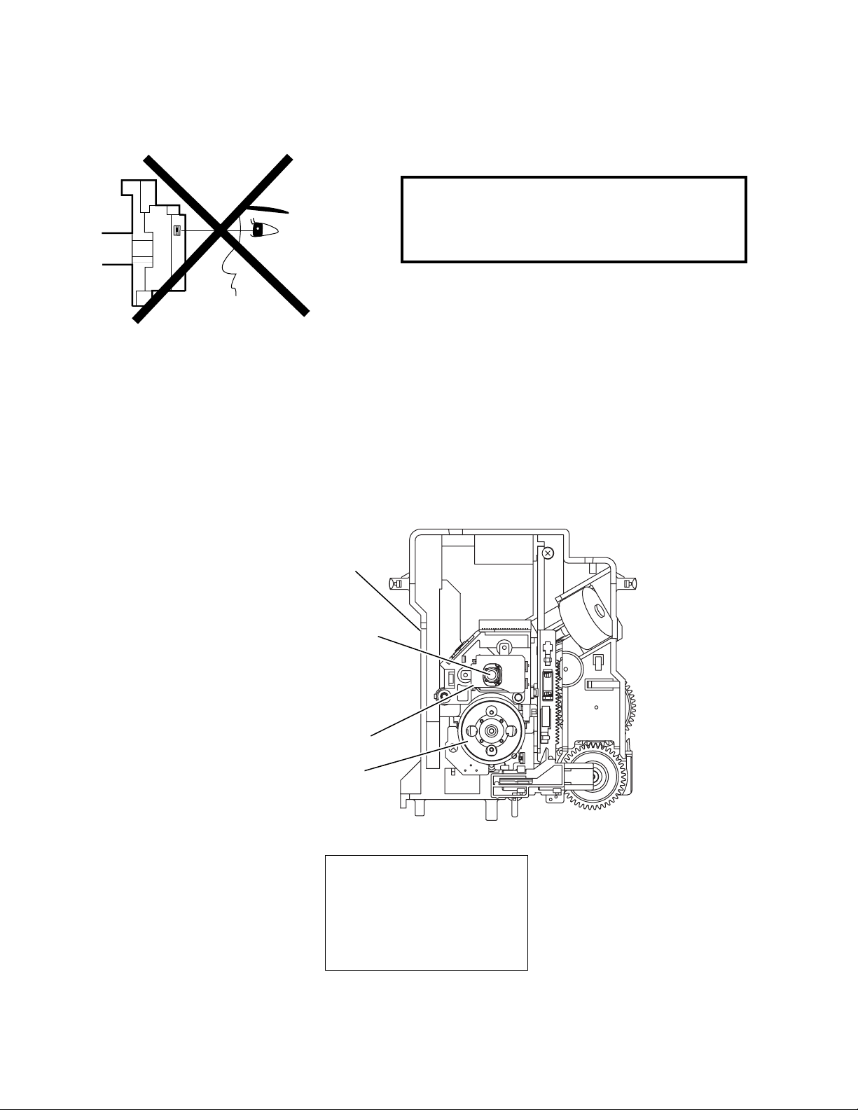
LASER BEAM SAFETY PRECAUTIONS
This DVD player uses a pickup that emits a laser beam.
Do not look directly at the laser beam coming
from the pickup or allow it to strike against your
skin.
The laser beam is emitted from the location shown in the figure. When checking the laser diode, be sure to keep
your eyes at least 30cm away from the pickup lens when the diode is turned on. Do not look directly at the laser
beam.
Caution: Use of controls and adjustments, or doing procedures other than those specified herein, may result in
hazardous radiation exposure.
Drive Mechanism Assembly
Laser Beam Radiation
Laser Pickup
Turntable
WHEN OPEN. DO NOT
CAUTION
LASER RADIATION
STARE INTO BEAM.
Location: Top of DVD mechanism.
1-2-1 TD300DC
Page 7
IMPORTANT SAFETY PRECAUTIONS
Prior to shipment from the factory, our products are strictly inspected for recognized product safety and electrical
codes of the countries in which they are to be sold. However, in order to maintain such compliance, it is equally
important to implement the following precautions when a set is being serviced.
Safety Precautions for TV Circuit
1. Before returning an instrument to the
customer, always make a safety check of the
entire instrument, including, but not limited to, the
following items:
a. Be sure that no built-in protective devices are
defective and have been defeated during
servicing. (1) Protective shields are provided
on this chassis to protect both the technician
and the customer. Correctly replace all missing
protective shields, including any removed for
servicing convenience. (2) When reinstalling
the chassis and/or other assembly in the
cabinet, be sure to put back in place all
protective devices, including but not limited to,
nonmetallic control knobs, insulating
fishpapers, adjustment and compartment
covers/shields, and isolation resistor/capacitor
networks. Do not operate this instrument or
permit it to be operated without all
protective devices correctly installed and
functioning. Servicers who defeat safety
features or fail to perform safety checks
may be liable for any resulting damage.
b. Be sure that there are no cabinet openings
through which an adult or child might be able to
insert their fingers and contact a hazardous
voltage. Such openings include, but are not
limited to, (1) spacing between the picture tube
and the cabinet mask, (2) excessively wide
cabinet ventilation slots, and (3) an improperly
fitted and/or incorrectly secured cabinet back
cover.
c. Antenna Cold Check - With the instrument AC
plug removed from any AC source, connect an
electrical jumper across the two AC plug
prongs. Place the instrument AC switch in the
on position. Connect one lead of an ohmmeter
to the AC plug prongs tied together and touch
the other ohmmeter lead in turn to each tuner
antenna input exposed terminal screw and, if
applicable, to the coaxial connector. If the
measured resistance is less than 1.0 megohm
or greater than 5.2 megohm, an abnormality
exists that must be corrected before the
instrument is returned to the customer. Repeat
this test with the instrument AC switch in the off
position.
d. Leakage Current Hot Check - With the
instrument completely reassembled, plug the
AC line cord directly into a 120 V AC outlet. (Do
not use an isolation transformer during this
test.) Use a leakage current tester or a
metering system that complies with American
National Standards Institute (ANSI) C101.1
Leakage Current for Appliances and
Underwriters Laboratories (UL) 1410, (50.7).
With the instrument AC switch first in the on
position and then in the off position, measure
from a known earth ground (metal water pipe,
conduit, etc.) to all exposed metal parts of the
instrument (antennas, handle brackets, metal
cabinet, screw heads, metallic overlays, control
shafts, etc.), especially any exposed metal
parts that offer an electrical return path to the
chassis. Any current measured must not
exceed 0.5 milli-ampere. Reverse the
instrument power cord plug in the outlet and
repeat the test.
READING SHOULD
NOT BE ABOVE 0.5 mA
LEAKAGE
DEVICE
BEING
TESTED
TEST ALL EXPOSED
METAL SURFACES
ALSO TEST WITH
PLUG REVERSED
USING AC
ADAPTER PLUG
AS REQUIRED
ANY MEASUREMENTS NOT WITHIN THE
LIMITS SPECIFIED HEREIN INDICATE A
POTENTIAL SHOCK HAZARD THAT MUST
BE ELIMINATED BEFORE RETURNING THE
INSTRUMENT TO THE CUSTOMER OR
BEFORE CONNECTING THE ANTENNA OR
ACCESSORIES.
e. X-Radiation and High Voltage Limits -
Because the picture tube is the primary
potential source of X-radiation in solid-state TV
receivers, it is specially constructed to prohibit
X-radiation emissions. For continued Xradiation protection, the replacement picture
tube must be the same type as the original.
CURRENT
TESTER
+
EARTH
GROUND
_
1-3-1 TVDVDN_ISP
Page 8

Also, because the picture tube shields and
mounting hardware perform an X-radiation
protection function, they must be correctly in
place. High voltage must be measured each
time servicing is performed that involves B+,
horizontal deflection or high voltage. Correct
operation of the X-radiation protection circuits
also must be reconfirmed each time they are
serviced. (X-radiation protection circuits also
may be called “horizontal disable” or “hold
down.”) Read and apply the high voltage limits
and, if the chassis is so equipped, the Xradiation protection circuit specifications given
on instrument labels and in the Product Safety
& X-Radiation Warning note on the service
data chassis schematic. High voltage is
maintained within specified limits by close
tolerance safety-related components/
adjustments in the high-voltage circuit. If high
voltage exceeds specified limits, check each
component specified on the chassis schematic
and take corrective action.
2. Read and comply with all caution and safetyrelated notes on or inside the receiver cabinet, on
the receiver chassis, or on the picture tube.
3. Design Alteration Warning - Do not alter or add
to the mechanical or electrical design of this TV
receiver. Design alterations and additions,
including, but not limited to circuit modifications
and the addition of items such as auxiliary audio
and/or video output connections, might alter the
safety characteristics of this receiver and create a
hazard to the user. Any design alterations or
additions will void the manufacturer's warranty and
may make you, the servicer, responsible for
personal injury or property damage resulting
therefrom.
4. Picture Tube Implosion Protection Warning -
The picture tube in this receiver employs integral
implosion protection. For continued implosion
protection, replace the picture tube only with one
of the same type number. Do not remove, install,
or otherwise handle the picture tube in any
manner without first putting on shatterproof
goggles equipped with side shields. People not so
equipped must be kept safely away while picture
tubes are handled. Keep the picture tube away
from your body. Do not handle the picture tube by
its neck. Some “in-line” picture tubes are equipped
with a permanently attached deflection yoke;
because of potential hazard, do not try to remove
such “permanently attached” yokes from the
picture tube.
5. Hot Chassis Warning a. Some TV receiver chassis are electrically
connected directly to one conductor of the AC
power cord and maybe safety-serviced without
an isolation transformer only if the AC power
plug is inserted so that the chassis is
connected to the ground side of the AC power
source. To confirm that the AC power plug is
inserted correctly, with an AC voltmeter,
measure between the chassis and a known
earth ground. If a voltage reading in excess of
1.0V is obtained, remove and reinsert the AC
power plug in the opposite polarity and again
measure the voltage potential between the
chassis and a known earth ground.
b. Some TV receiver chassis normally have 85V
AC(RMS) between chassis and earth ground
regardless of the AC plug polarity. This chassis
can be safety-serviced only with an isolation
transformer inserted in the power line between
the receiver and the AC power source, for both
personnel and test equipment protection.
c. Some TV receiver chassis have a secondary
ground system in addition to the main chassis
ground. This secondary ground system is not
isolated from the AC power line. The two
ground systems are electrically separated by
insulation material that must not be defeated or
altered.
6. Observe original lead dress. Take extra care to
assure correct lead dress in the following areas: a.
near sharp edges, b. near thermally hot parts-be
sure that leads and components do not touch
thermally hot parts, c. the AC supply, d. high
voltage, and, e. antenna wiring. Always inspect in
all areas for pinched, out of place, or frayed wiring.
Check AC power cord for damage.
7. Components, parts, and/or wiring that appear to
have overheated or are otherwise damaged
should be replaced with components, parts, or
wiring that meet original specifications.
Additionally, determine the cause of overheating
and/or damage and, if necessary, take corrective
action to remove any potential safety hazard.
8. Product Safety Notice - Some electrical and
mechanical parts have special safety-related
characteristics which are often not evident from
visual inspection, nor can the protection they give
necessarily be obtained by replacing them with
components rated for higher voltage, wattage, etc..
Parts that have special safety characteristics are
identified by a # on schematics and in parts lists.
Use of a substitute replacement that does not
have the same safety characteristics as the
recommended replacement part might create
shock, fire, and/or other hazards. The product's
safety is under review continuously and new
instructions are issued whenever appropriate.
Prior to shipment from the factory, our products
are strictly inspected to confirm they comply with
the recognized product safety and electrical codes
1-3-2 TVDVDN_ISP
Page 9

of the countries in which they are to be sold.
However, in order to maintain such compliance, it
is equally important to implement the following
precautions when a set is being serviced.
Precautions during Servicing
A. Parts identified by the # symbol are critical for
safety.
Replace only with part number specified.
B. In addition to safety, other parts and assemblies
are specified for conformance with regulations
applying to spurious radiation. These must also be
replaced only with specified replacements.
Examples: RF converters, RF cables, noise
blocking capacitors, and noise blocking filters, etc.
C. Use specified internal wiring. Note especially:
1) Wires covered with PVC tubing
2) Double insulated wires
3) High voltage leads
D. Use specified insulating materials for hazardous
live parts. Note especially:
1) Insulation Tape
2) PVC tubing
3) Spacers
4) Insulators for transistors.
E. When replacing AC primary side components
(transformers, power cord, etc.), wrap ends of
wires securely about the terminals before
soldering.
F. Observe that the wires do not contact heat
producing parts (heat sinks, oxide metal film
resistors, fusible resistors, etc.)
G. Check that replaced wires do not contact sharp
edged or pointed parts.
H. When a power cord has been replaced, check that
5~6 kg of force in any direction will not loosen it.
I. Also check areas surrounding repaired locations.
J. Be careful that foreign objects (screws, solder
droplets, etc.) do not remain inside the set.
K. Crimp type wire connector
When replacing the power transformer in sets
where the connections between the power cord
and power transformer primary lead wires are
performed using crimp type connectors, in order to
prevent shock hazards, perform carefully and
precisely the following steps.
Replacement procedure
1) Remove the old connector by cutting the wires
at a point close to the connector.
Important: Do not re-use a connector (discard
it).
2) Strip about 15 mm of the insulation from the
ends of the wires. If the wires are stranded,
twist the strands to avoid frayed conductors.
3) Align the lengths of the wires to be connected.
Insert the wires fully into the connector.
4) Use the crimping tool to crimp the metal sleeve
at the center position. Be sure to crimp fully to
the complete closure of the tool.
L. When connecting or disconnecting the DVD/VCR
connectors, first, disconnect the AC plug from the
AC supply socket.
1-3-3 TVDVDN_ISP
Page 10
Safety Check after Servicing
Examine the area surrounding the repaired location for damage or deterioration. Observe that screws, parts and
wires have been returned to original positions. Afterwards, perform the following tests and confirm the specified
values in order to verify compliance with safety standards.
1. Clearance Distance
When replacing primary circuit components, confirm
specified clearance distance (d) and (d') between
soldered terminals, and between terminals and
surrounding metallic parts. (See Fig. 1)
Table 1: Ratings for selected area
Chassis or Secondary Conductor
Primary Circuit Terminals
AC Line Voltage Region
110 to 130 V
Note: This table is unofficial and for reference only. Be
sure to confirm the precise values.
U.S.A. or
Canada
Clearance
Distance (d), (d’)
≥ 3.2 mm
(0.126 inches)
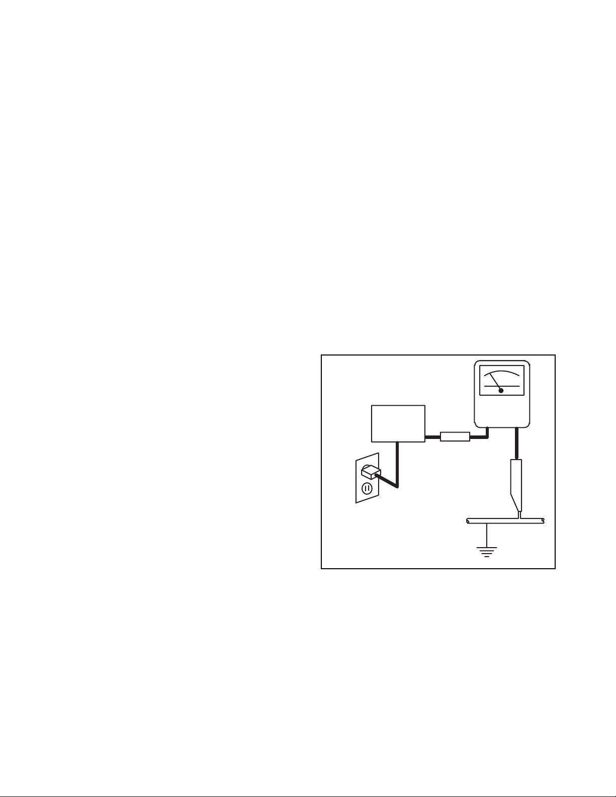
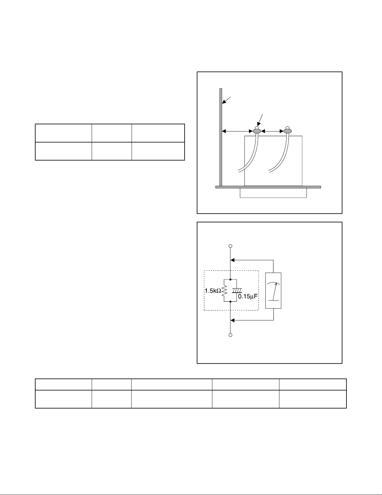
2. Leakage Current Test
Confirm the specified (or lower) leakage current
between B (earth ground, power cord plug prongs) and
externally exposed accessible parts (RF terminals,
antenna terminals, video and audio input and output
terminals, microphone jacks, earphone jacks, etc.).
Measuring Method: (Power ON)
Insert load Z between B (earth ground, power cord plug
prongs) and exposed accessible parts. Use an AC
voltmeter to measure across both terminals of load Z.
See Fig. 2 and following table.
dd'
Fig. 1
Exposed Accessible Part
Z
AC Voltmeter
(High Impedance)
Earth Ground
B
Power Cord Plug Prongs
Fig. 2
Table 2: Leakage current ratings for selected areas
AC Line Voltage Region Load Z Leakage Current (i) Earth Ground (B) to:
110 to 130 V
Note: This table is unofficial and for reference only. Be sure to confirm the precise values.
U.S.A. or
Canada
0.15 µF CAP. & 1.5 kΩ
RES. Connected in parallel
1-3-4 TVDVDN_ISP
i ≤ 0.5 mA rms
Exposed accessible
parts
Page 11
STANDARD NOTES FOR SERVICING
Circuit Board Indications
1. The output pin of the 3 pin Regulator ICs is
indicated as shown.
Top View
Out
2. For other ICs, pin 1 and every fifth pin are
indicated as shown.
Pin 1
3. The 1st pin of every male connector is indicated as
shown.
Input
In
Bottom View
5
10
Pb (Lead) Free Solder
Pb free mark will be found on PCBs which use Pb
free solder. (Refer to figure.) For PCBs with Pb free
mark, be sure to use Pb free solder. For PCBs
without Pb free mark, use standard solder.
Pb free mark
How to Remove / Install Flat Pack-IC
1. Removal
With Hot-Air Flat Pack-IC Desoldering Machine:
1. Prepare the hot-air flat pack-IC desoldering
machine, then apply hot air to the Flat Pack-IC
(about 5 to 6 seconds). (Fig. S-1-1)
Pin 1
Instructions for Connectors
1. When you connect or disconnect the FFC (Flexible
Foil Connector) cable, be sure to first disconnect
the AC cord.
2. FFC (Flexible Foil Connector) cable should be
inserted parallel into the connector, not at an
angle.
FFC Cable
Connector
CBA
* Be careful to avoid a short circuit.
Fig. S-1-1
2. Remove the flat pack-IC with tweezers while
applying the hot air.
3. Bottom of the flat pack-IC is fixed with glue to the
CBA; when removing entire flat pack-IC, first apply
soldering iron to center of the flat pack-IC and heat
up. Then remove (glue will be melted). (Fig. S-1-6)
4. Release the flat pack-IC from the CBA using
tweezers. (Fig. S-1-6)
CAUTION:
1. The Flat Pack-IC shape may differ by models. Use
an appropriate hot-air flat pack-IC desoldering
machine, whose shape matches that of the Flat
Pack-IC.
2. Do not supply hot air to the chip parts around the
flat pack-IC for over 6 seconds because damage
to the chip parts may occur. Put masking tape
1-4-1 TVDVDN_SN
Page 12
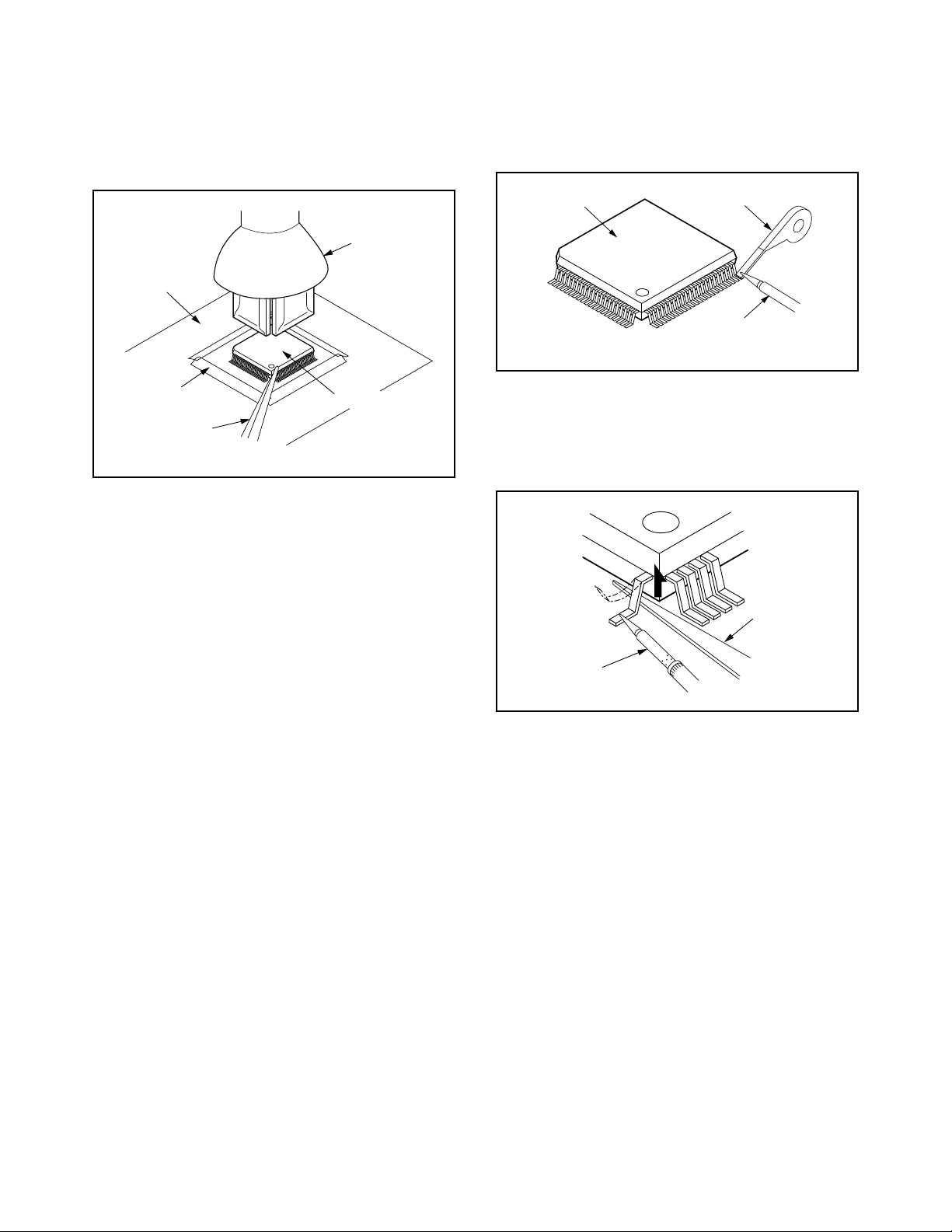
around the flat pack-IC to protect other parts from
damage. (Fig. S-1-2)
3. The flat pack-IC on the CBA is affixed with glue, so
be careful not to break or damage the foil of each
pin or the solder lands under the IC when
removing it.
Hot-air
Flat Pack-IC
Desoldering
CBA
Machine
With Soldering Iron:
1. Using desoldering braid, remove the solder from
all pins of the flat pack-IC. When you use solder
flux which is applied to all pins of the flat pack-IC,
you can remove it easily. (Fig. S-1-3)
Flat Pack-IC
Desoldering Braid
Soldering Iron
Fig. S-1-3
Masking
Tape
Tweezers
Flat Pack-IC
Fig. S-1-2
2. Lift each lead of the flat pack-IC upward one by
one, using a sharp pin or wire to which solder will
not adhere (iron wire). When heating the pins, use
a fine tip soldering iron or a hot air desoldering
machine. (Fig. S-1-4)
Sharp
Pin
Fine Tip
Soldering Iron
3. Bottom of the flat pack-IC is fixed with glue to the
CBA; when removing entire flat pack-IC, first apply
soldering iron to center of the flat pack-IC and heat
up. Then remove (glue will be melted). (Fig. S-1-6)
4. Release the flat pack-IC from the CBA using
tweezers. (Fig. S-1-6)
Fig. S-1-4
1-4-2 TVDVDN_SN
Page 13
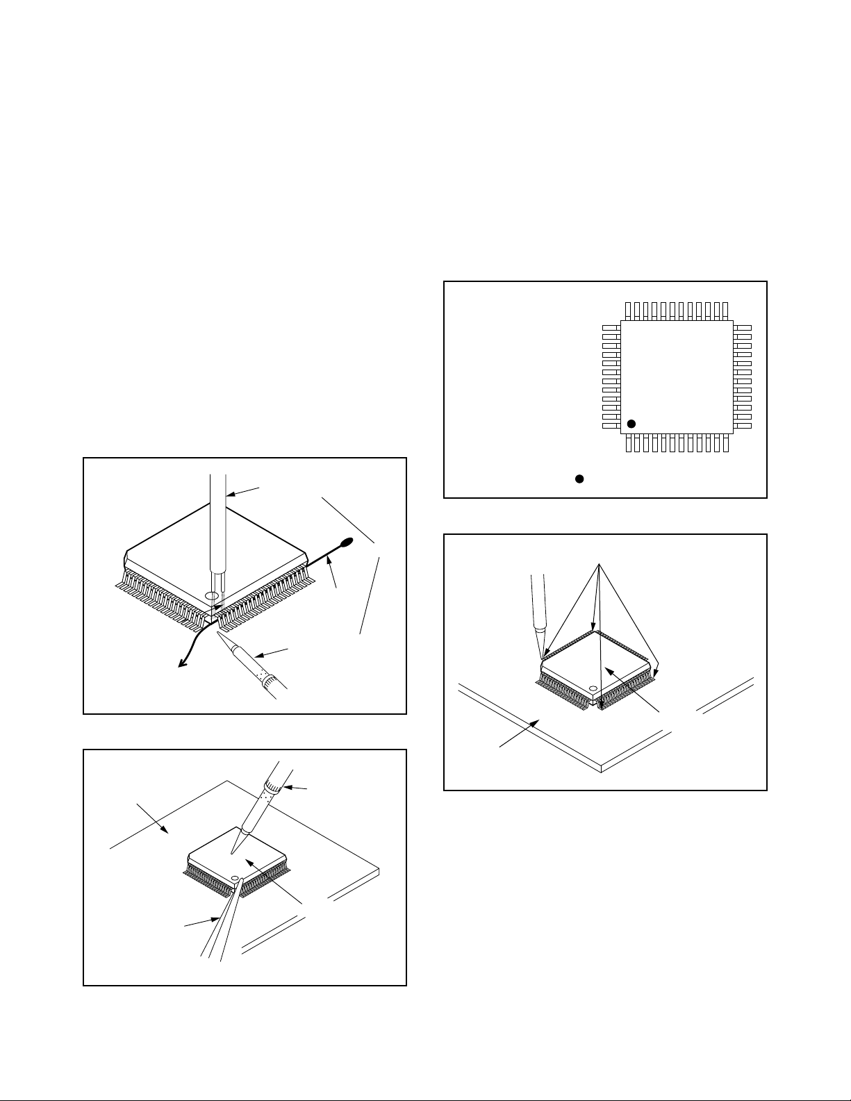
With Iron Wire:
1. Using desoldering braid, remove the solder from
all pins of the flat pack-IC. When you use solder
flux which is applied to all pins of the flat pack-IC,
you can remove it easily. (Fig. S-1-3)
2. Affix the wire to a workbench or solid mounting
point, as shown in Fig. S-1-5.
3. While heating the pins using a fine tip soldering
iron or hot air blower, pull up the wire as the solder
melts so as to lift the IC leads from the CBA
contact pads as shown in Fig. S-1-5.
4. Bottom of the flat pack-IC is fixed with glue to the
CBA; when removing entire flat pack-IC, first apply
soldering iron to center of the flat pack-IC and heat
up. Then remove (glue will be melted). (Fig. S-1-6)
5. Release the flat pack-IC from the CBA using
tweezers. (Fig. S-1-6)
Note: When using a soldering iron, care must be
taken to ensure that the flat pack-IC is not
being held by glue. When the flat pack-IC is
removed from the CBA, handle it gently
because it may be damaged if force is applied.
Hot Air Blower
2. Installation
1. Using desoldering braid, remove the solder from
the foil of each pin of the flat pack-IC on the CBA
so you can install a replacement flat pack-IC more
easily.
2. The “●” mark on the flat pack-IC indicates pin 1.
(See Fig. S-1-7.) Be sure this mark matches the 1
on the PCB when positioning for installation. Then
presolder the four corners of the flat pack-IC. (See
Fig. S-1-8.)
3. Solder all pins of the flat pack-IC. Be sure that
none of the pins have solder bridges.
Example :
Pin 1 of the Flat Pack-IC
is indicated by a " " mark.
Fig. S-1-7
To Solid
Mounting Point
CBA
Tweezers
Iron Wire
Soldering Iron
Fig. S-1-5
Fine Tip
Soldering Iron
Flat Pack-IC
or
Presolder
Flat Pack-IC
CBA
Fig. S-1-8
Fig. S-1-6
1-4-3 TVDVDN_SN
Page 14
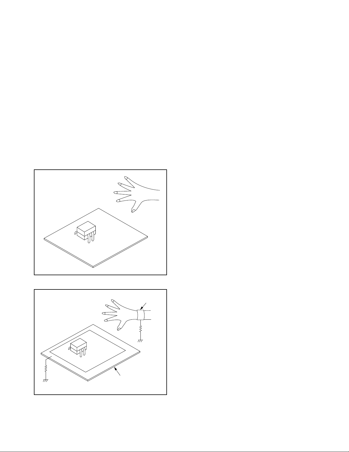
Instructions for Handling Semiconductors
Electrostatic breakdown of the semi-conductors may
occur due to a potential difference caused by
electrostatic charge during unpacking or repair work.
1. Ground for Human Body
Be sure to wear a grounding band (1 MΩ) that is
properly grounded to remove any static electricity that
may be charged on the body.
2. Ground for Workbench
Be sure to place a conductive sheet or copper plate
with proper grounding (1 MΩ) on the workbench or
other surface, where the semi-conductors are to be
placed. Because the static electricity charge on
clothing will not escape through the body grounding
band, be careful to avoid contacting semi-conductors
with your clothing.
<Incorrect>
<Correct>
1MΩ
CBA
Grounding Band
1MΩ
CBA
Conductive Sheet or
Copper Plate
1-4-4 TVDVDN_SN
Page 15
CABINET DISASSEMBLY INSTRUCTIONS
1. Disassembly Flowchart
This flowchart indicates the disassembly steps for the
cabinet parts, and the CBA in order to gain access to
item(s) to be serviced. When reassembling, follow the
steps in reverse order. Bend, route and dress the
cables as they were.
CAUTION!
When removing the CRT, be sure to discharge the
Anode Lead of the CRT with the CRT Ground Wire
before removing the Anode Cap.
[1] Rear Cabinet
[10] H.V./
DC Power
Supply
CBA
[7] DVD
Junction
CBA
[4] CRT
[8] DVD
Main
CBA
Unit
[2] H.V. CBA (with Holder)
[3] Tray Chassis Unit
[5] Shield Box
[6] DVD Mechanism
[9] Main CBA
2. Disassembly Method
REMOVAL
ID/
LOC.
No.
[1]
[2]
[3]
[4] CRT 2 4(S-5) [5] Shield Box 3 5(S-6) -
[6]
[7]
[8]
[9] Main CBA 3, 5 4(S-9) -
[10]
PA RT
Rear
Cabinet
H.V. CBA
(With
Holder)
Tr ay
Chassis
Unit
DVD
Mechanism
DVD
Junction
CBA
DVD Main
CBA Unit
H.V./DC
Power
Supply
CBA
REMOVE/
*UNHOOK/UNLOCK/
Fig.
No.
RELEASE/UNPLUG/
DESOLDER
1 4(S-1), 1(S-2), 2(S-3) -
4(S-4), Anode Cap,
CN501, CRT CBA,
3, 5
CN571, WH551,
WH552, WH554
3, 5 CN1802, CN1801 -
3, 4, 5 2(S-7A), 3(S-7B),
CN401, CN601
3, 5 (S-7C), CN1603 -
2(S-8), CN201,
4, 5
CN301
7(S-10), (S-11),
Shield Case Top,
3, 5
Shield Case Bottom,
FBT Holder
Note
1
-
2
3
-
↓
(1)
Note:
(1) Order of steps in procedure. When reassembling,
follow the steps in reverse order. These numbers
are also used as the Identification (location) No. of
parts in figures.
(2) Parts to be removed or installed.
(3) Fig. No. showing procedure of part location
(4) Identification of parts to be removed, unhooked,
unlocked, released, unplugged, unclamped, or
desoldered.
P = Spring, L = Locking Tab, S = Screw,
CN = Connector
* = Unhook, Unlock, Release, Unplug, or Desolder
e.g. 2(S-2) = two Screws (S-2),
2(L-2) = two Locking Tabs (L-2)
(5) Refer to the following “Reference Notes in the
Ta bl e ” .
1-5-1 TD300DC
↓
(2)
↓
(3)
↓
(4)
↓
(5)
Page 16
Reference Notes in the Table
CAUTION!
When removing the CRT, be sure to discharge the
Anode Lead of the CRT with the CRT Ground Wire
before removing the Anode Cap.
1. CAUTION 1: Discharge the Anode Lead of the
CRT with the CRT Ground Wire before removing
the Anode Cap.
Disconnect the following: Anode Cap, CN501,
CRT CBA, CN571, WH551, WH552, WH554.
Then remove H.V. CBA (with Holder).
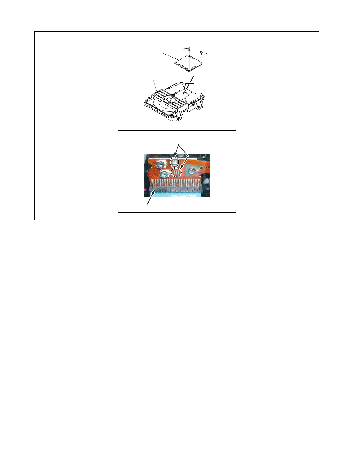
2. CAUTION 2: Electrostatic breakdown of the laser
diode in the optical system block may occur as a
potential difference caused by electrostatic charge
accumulated on cloth, human body etc., during
unpacking or repair work.
To avoid damage of pickup follow next procedures.
1) Disconnect Connector (CN301) on the DVD
Main CBA Unit.
2) Short the three short lands of FPC cable with
solder before removing the FFC cable (CN201)
from it. If you disconnect the FFC cable
(CN201), the laser diode of pickup will be
destroyed. (Fig. D4)
3) To remove the DVD Main CBA Unit, remove
two screws (S-8).
3. CAUTION 3: When reassembling, confirm the
FFC cable (CN201) is connected completely. Then
remove the solder from the three short lands of
FPC cable. (Fig. D4)
S-1
S-2
S-3
S-1
[4] CRT
S-5
[1] Rear Cabinet
Anode Cap
S-5
S-1
Fig. 1
CRT CBA
S-5
S-5
Fig. 2
1-5-2 TD300DC
Page 17
S-6
S-6
[3] Tray Chassis Unit
[5] Shield
Box
S-7C
[7] DVD
Junction
CBA
S-9
S-7A
S-7B
S-9
S-9
S-6
S-7B
[6] DVD
Mechanism
S-7A
[9] Main CBA
S-9
S-10
[10] H.V./DC
Power
Supply CBA
Shield Case Top
S-10
Shield
Case
Bottom
FBT Holder
S-4
S-10
S-11
[2] H.V. CBA
(wih Holder)
1-5-3 TD300DC
S-4
Fig. 3
Page 18
[8] DVD Main
CBA Unit
S-8
S-8
DVD Mechanism
Short the three short lands by soldering.
(Either of two places.)
Connector
View for A
A
Fig. D4
1-5-4 TD300DC
Page 19
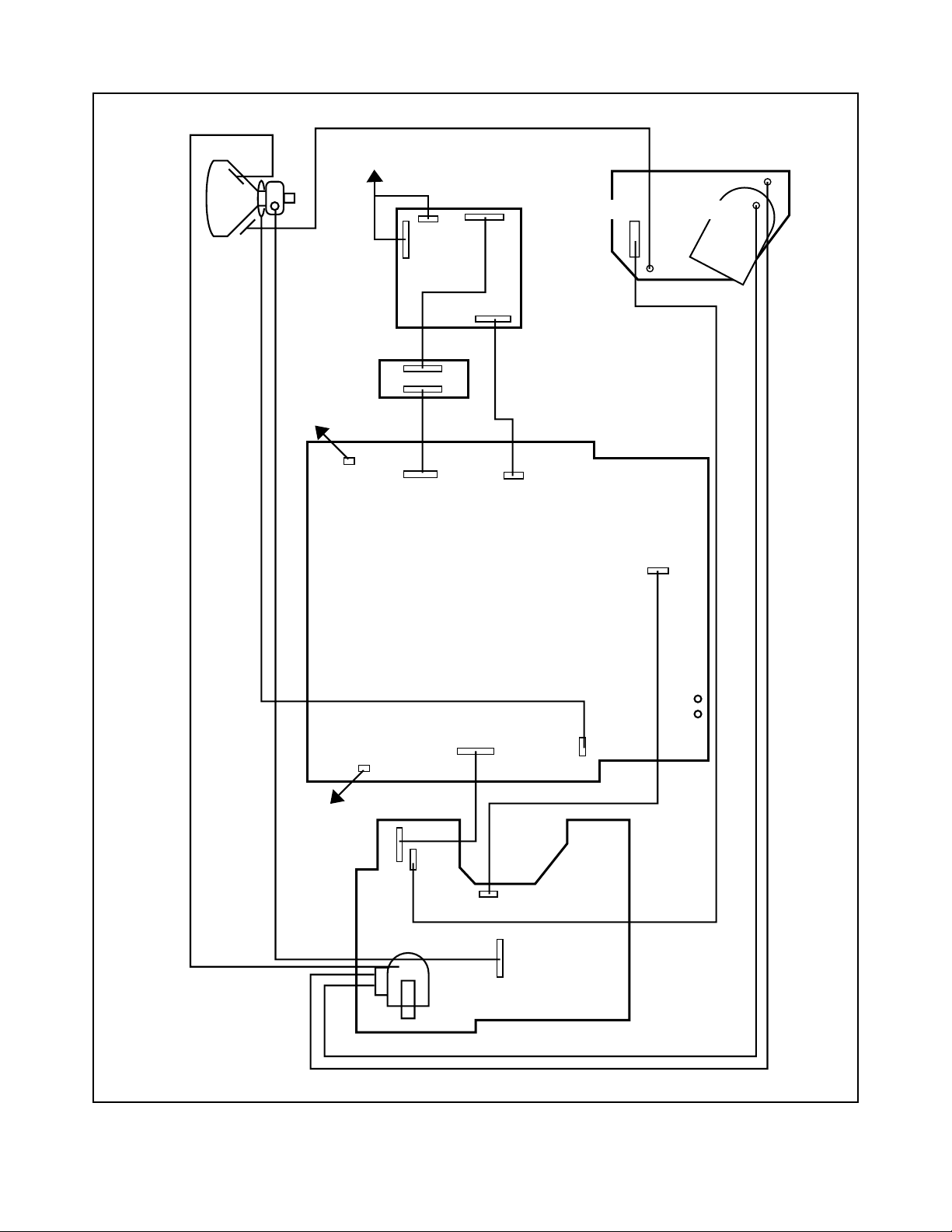
ANODE
CRT
GND
DVD MECHANISM
CN301
CN201
CN401
CN601
WH501
DVD MAIN
CBA UNIT
CRT CBA
SCREEN
FOCUS
CN501
DVD JUNCTION
CBA
SPEAKER
CN1802
CN1603
MAIN CBA
CN1801
CN2603B
CN2603A
CN1302
CN1731
CN1604
CN1601
AC
CORD
SPEAKER
WH552
WH551
WH554A
CN571
H.V./DC
POWER
SUPPLY
CBA
1-5-5 TD300DC
Fig. 5
Page 20
ELECTRICAL ADJUSTMENT INSTRUCTIONS
General Note:
"CBA" is abbreviation for "Circuit Board
Assembly."
NOTE:
Electrical adjustments are required after replacing circuit components and certain mechanical parts.
It is important to perform these adjustments only after
all repairs and replacements have been completed.
Also, do not attempt these adjustments unless the
proper equipment is available.
Test Equipment Required
1. NTSC Pattern Generator (Color Bar W/White Window, Red Color, Dot Pattern, Gray Scale, Monoscope, Multi-Burst)
2. AC Milli Voltmeter (RMS)
3. DC Voltmeter
4. Oscilloscope: Dual-trace with 10:1 probe,
V-Range: 0.001~50V/Div,
F-Range: DC~AC-60MHz
5. Frequency Counter
6. Plastic Tip Driver
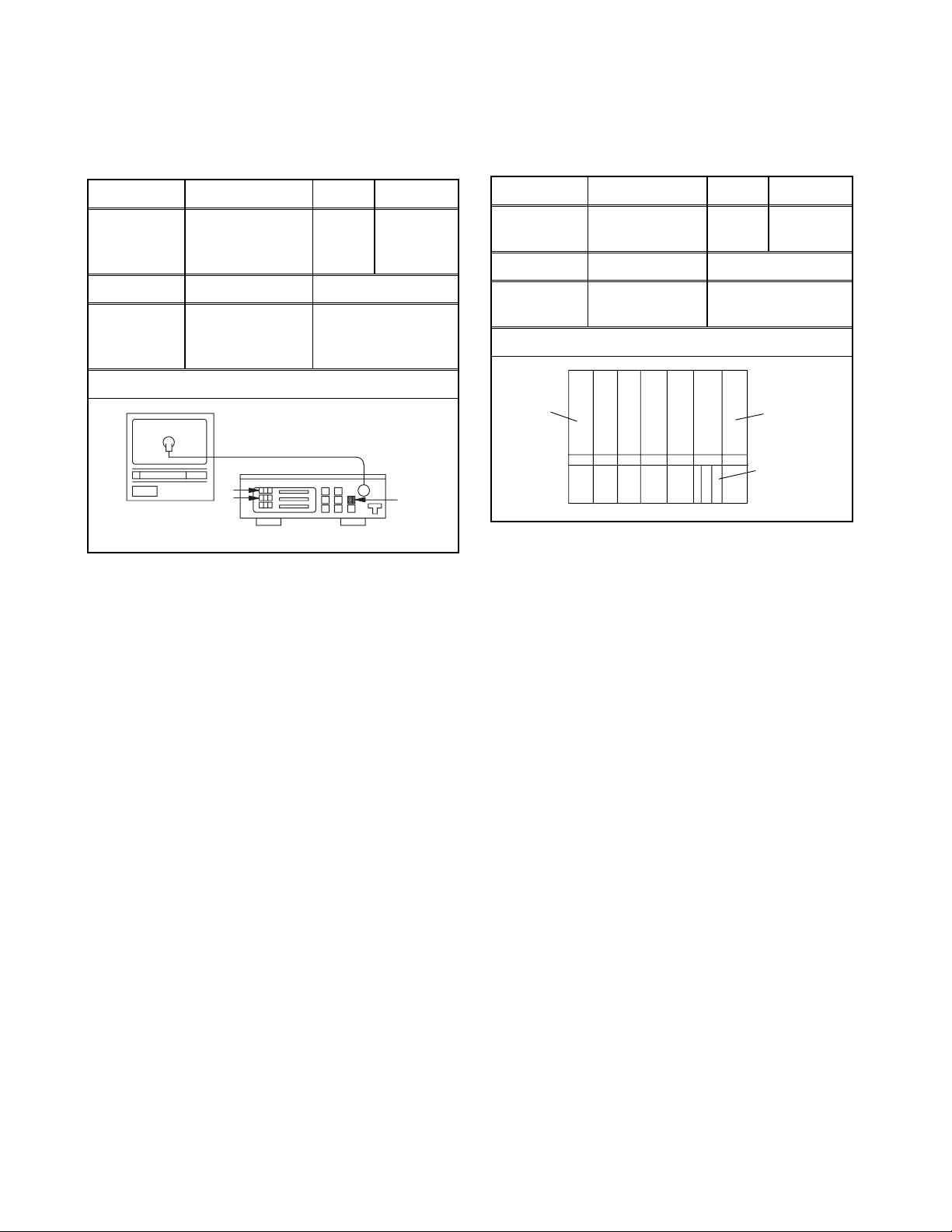
How to make service remote control
unit:
1. Prepare remote control unit. (Part No. NE200UD or
NE207UD) Remove 4 screws from the back lid.
(Fig. 1-1)
SCREW
How to Set up the Service mode:
Service Mode:
1. Use the service remote control unit.
2. Turn the power on.
3. Press [DISC MENU] button on the service remote
control unit.
1a. DC 117V (+B) Adjustment
(AC Power)
Purpose: To obtain correct operation.
Symptom of Misadjustment: The picture is dark and
unit does not operate correctly.
Test point Adj. Point Mode Input
J109 (+B)
TP1303 (GND)
Tape M. EQ. Spec.
---
Note: J109 (+B) --- HV/DC Power Supply CBA
TP1303 (GND), VR1601 --- Main CBA
1. Connect the unit to AC Power Outlet.
2. Connect DC Volt Meter to J109 (+B) and TP1303
(GND).
3. Adjust VR1601 so that the voltage of J109 (+B)
becomes +117±0.5V DC.
VR1601 --- -----
DC Voltmeter
Plastic Tip Driver
+117±0.5V DC
Remote control unit (Bottom)
2. Remote control unit: Part No. NE200UD or
NE207UD
Cut off pin 10 of the remote control microprocessor
and short circuit pins 10 and 17 of the microprocessor with a jumper wire.
Fig. 1-1
1-6-1 TD300EA
Page 21

1b. DC 117V (+B) Adjustment
3-1. Setting for Data Values
(DC Power)
Purpose: To obtain correct operation.
Symptom of Misadjustment: The picture is dark and
unit does not operate correctly.
Test point Adj. Point Mode Input
J109 (+B)
TP1303 (GND)
Tape M. EQ. Spec.
---
Note: J109(+B), VR951 --- HV/DC Power Supply CBA
TP1303(GND) --- Main CBA
1. Input 13.2V DC to DC Jack.
2. Connect DC Volt Meter to J109(+B) and
TP1303(GND).
3. Adjust VR1951 so that the voltage of J109(+B)
becomes +117±0.5V DC.
VR951 --- -----
DC Voltmeter
Plastic Tip Driver
+117±0.5V DC
2. Black Stretch Control Adjustment
Purpose: To show the fine black color.
Symptom of Misadjustment: Black color will not
appear correctly.
Note: Use service remote control unit.
1. Enter the Service mode. (See page 1-6-1)
2. Press [6] button on the service remote control unit.
"B-S" is indicated.
3. Press [CH o / p] buttons on the service remote con-
trol unit so that display will change "OFF," "0," "1," "2"
and "3." Then choose "B-S OFF."
4. Press [6] button on the service remote control unit.
"BS-2" is indicated.
5. Press [CH o / p] buttons on the service remote
control unit so that display will change "0," "1," "2"
and "3." Then choose "BS-2 0."
6. Turn the power off and on again, using the main
power button on the TV unit.
General
1. Enter the Service mode. (See page 1-6-1)
2. To select the Data Value, press [VOL p] button on
the service remote control unit.
3. To set the following each data value, press [CH o
/ p] buttons on the service remote control unit.
7F --- set to FF
3-2. Setting for CONTRAST,
COLOR, TINT and V-TINT
data Values
General
1. Enter the Service mode. (See page 1-6-1)
2. Press [PICTURE" button on the service remote control
unit. Display changes "BRIGHT," "CONTRAST,"
"COLOR," "TINT," and "V-TINT" cyclically when [PICTURE] button is pressed.
CONTRAST (CNT)
1. Press [PICTURE] button on the service remote control unit. Then select "CONTRAST" (CNT) display.
2. Press [CH o / p] buttons on the service remote
control unit so that the value of "CONTRAST"
(CNT) becomes 76.
COLOR (CLR)
1. Press [PICTURE] button on the service remote
control unit. Then select "COLOR" (CLR) display.
2. Press [CH o / p] buttons on the service remote
control unit so that the value of "COLOR" (CLR)
becomes 55.
TINT (TNT)
1. Press [PICTURE] button on the service remote
control unit. Then select "TINT" (TNT) display.
2. Press [CH o / p] buttons on the service remote
control unit so that the value of "TINT" (TNT) becomes 64.
V-TINT (V-TNT)
1. Press [PICTURE] button on the service remote
control unit. Then select "V-TINT" (V-TNT) display.
2. Press [CH o / p] buttons on the service remote
control unit so that the value of "V-TINT" (V-TNT)
becomes 57.
Note: BRIGHT data value does not need to be adjust-
ed at this moment.
1-6-2 TD300EA
Page 22
4. V. Size Adjustment
6. H. Position Adjustment
Purpose: To obtain correct vertical height of screen
image.
Symptom of Misadjustment: If V. Size is incorrect,
vertical height of image on the screen may not be
properly displayed.
Test point Adj. Point Mode Input
---
Tape M. EQ. Spec.
--- Pattern Generator 90±5%
1. Enter the Service mode. (See page 1-6-1.)
Press [9] button on the remote control unit and
select V-S Mode. (Press [9] button then display will
change to V-P and V-S).
2. Input monoscope pattern.
3. Press [CH o / p] buttons on the remote control
unit so that the monoscope pattern is 90±5% of
display size and the circle is round.
CH o / p
buttons
--- Monoscope
5. V. Position Adjustment
Purpose: To obtain correct vertical width of screen
image.
Symptom of misadjustment: If V. Position is incor-
rect, vertical height of image on the screen may not be
properly displayed.
Purpose: To obtain correct horizontal position of
screen image.
Symptom of Misadjustment: If H. Position is incorrect, horizontal position of image on the screen may
not be properly displayed.
Test Point Adj. Point Mode Input
CH o / p
---
Tape M. EQ. Spec.
--- Monoscope 90±5%
Note: Use service remote control unit
1. Operate the unit for at least 20 minutes.
2. Enter the Service mode. (See page 1-6-1)
3. Receive the Monoscope Pattern.
4. Press [8] button on the remote control unit and select "H-P" mode.
5. Press [CH o / p] buttons on the service remote
control unit so that the monoscope pattern will be
90±5% of display size and the circle is round.
6. Turn the power off and on again, using the main
power button on the TV unit.
buttons
[ H-P ] Mode
RF
Monoscope
Test point Adj. Point Mode Input
Screen Control,
---
Tape M. EQ. Spec.
--- Pattern Generator 90±5%
Note: Use service remote control unit
1. Operate the unit for at least 20 minutes.
2. Enter the Service Mode. (See page 1-6-1)
3. Receive the Monoscope Pattern.
4. Press [9] button on the service remote control unit
and select "V-P" mode. (Display change "V-S" and
"V-P" cyclically when [9] button is pressed.)
5. Press [CH o / p] buttons on the service remote
control unit so that the top and bottom of the monoscope pattern will be equal of each other.
6. Turn the power off and on again, using the main
power button on the TV unit.
CH o / p
buttons
RF Monoscope
1-6-3 TD300EA
Page 23
7. White Balance Adjustment
Purpose: To mix red, green and blue beams correctly
for pure white.
Symptom of Misadjustment: White becomes bluish
or reddish.
8. Sub-Brightness Adjustment
Purpose: To get proper brightness.
Symptom of Misadjustment: If Sub-Brightness is
incorrect, proper brightness cannot be obtained by
adjusting the Brightness Control.
Test Point Adj. Point Mode Input
Screen
Tape M. EQ. Spec.
Note: Use service remote control unit
1. Operate the unit more than 20 minutes.
2. Face the unit to east. Degauss the CRT using Degaussing Coil.
3. Input the White Raster (APL 100%).
4. Set the color analyzer to the CHROMA mode and
after zero point calibration, bring the optical receptor to the center on the tube surface (CRT).
5. Enter the Service mode. Press [VOL p] button on
the service remote control unit and select "C/D"
mode. (Display changes "C/D," "7F," and "DVDKEY" cyclically when [VOL p" button is pressed.)
Then press [8] button on the Service remote control Unit.
6. Press [4] button on the service remote control unit
for Red adjustment. Press [5] button on the service
remote control unit for Blue adjustment.
7. In each color mode, press [CH o / p] button to adjust the values of color.
8. Adjusting Red and Blue color so that the temperature becomes 9200K (x: 286 / y: 294) ±3%.
9. At this time, re-check that Horizontal line is white.
If not, Re-adjust Cut-off Adjustment until the Horizontal Line becomes pure white.
10. Turn off and on again to return to normal mode. Receive APL 100% white signal and Check Chroma
temperatures become 9200K (x: 286 / y: 294) ±3%.
Note: Confirm that Cut Off Adj. is correct after this
adjustment, and attempt Cut Off Adj. if needed.
CH o / p
buttons
Pattern
Generator,
Color analyzer
Figure
Color Analyzer
RF
See below
White Ras-
ter (APL
100%)
Fig. 2
Test Point Adj. Point Mode Input
---
Tape M. EQ. Spec.
---
White
Note: IQW Setup level --- 7.5 IRE
Use service remote control unit
1. Enter the Service mode. (See page 1-6-1)
Then input IQW signal from RF Input.
2. Press [PICTURE] button on the service remote control unit and Select "BRT" mode. (Display changes
"BRT," "CNT," "CLR," "TNT," and "V-TINT" cyclically when PICTURE button is pressed.) Press [CH
o / p] buttons so that the bar is just visible (See
above figure).
3. Turn the power off and on again, using the main
power button on the TV unit.
CH o / p
buttons
Pattern
Generator
Figure
RF IQW
See below
Black
This bar
just
visible
Fig. 3
1-6-4 TD300EA
Page 24

9. Focus Adjustment
10. C-Trap Adjustment
Purpose: Set the optimum Focus.
Symptom of Misadjustment: If Focus Adjustment is
incorrect, blurred images are shown on the display.
Test Point Adj. Point Mode Input
--- Focus Control RF
Tape M. EQ. Spec.
---
Note: Focus VR (FBT) --- HV/DC Power Supply CBA
FBT= Fly Back Transformer
1. Operate the unit more than 30 minutes
2. Face the unit to the East and degauss the CRT using a degaussing coil.
3. Input the Monoscope Pattern.
4. Adjust the Focus Control on the FBT to obtain clear
picture.
Pattern
Generator
Mono-
scope
See below
Purpose: To get minimum leakage of the color signal
carrier.
Symptom of Misadjustment: If C-Trap Adjustment is
incorrect, stripes will appear on the screen.
Test point Adj. Point Mode Input
D1311
Cathode
(B-OUT)
Tap e M. E Q. Spec.
---
minimum
Note: D1311 Cathode (B-Out)--- Main CBA
1. Connect Oscilloscope to D1311 Cathode.
2. Input a color bar signal from RF input.
Enter the Service mode. (See page 1-6-1.)
3. Press [0] button on the remote control unit and
select C-TRAP Mode.
4. Press [CH o / p] buttons on the remote control
unit so that the carrier leakage B-Out (3.58MHz)
value becomes minimum on the oscilloscope.
5. Turn the power off and on again.
CH o / p
buttons
Oscilloscope
Pattern Generator
Figure
--- Color Bar
---
Fig. 4
1-6-5 TD300EA
Page 25

11. H f0 Adjustment
Purpose: To get correct horizontal frequency.
Symptom of Misadjustment: If H f0 adjustment is in
correct, skew distortion will appear on the screen.
Test Point Adj. Point Mode Input
R583
Tape M. EQ. Spec.
---
Note: R583 --- HV/DC Power Supply CBA
Use Service remote control unit.
1. Connect Frequency Counter to R583 and ground.
2. Set the unit to the VIDEO mode which is located before CH2 and no input is necessary. Enter the Service mode. (See page 1-6-1)
3. Operate the unit for at least 20 minutes.
4. Press [2] button on the Service remote control unit
and select H-ADJ Mode. (By pressing [2] button the
display will change from TV AGC to H-ADJ.)
5. Press [CH o / p] button on the Service remote con-
trol unit so that the display will change "0" ~ "7." At
this moment, Choose display one of them from "0"
~ "7" when the Frequency Counter shows 15.734
kHz±300Hz or closer.
6. Turn the power off and on again. (Main Power button on the TV unit.)
CH o / p button
["H-ADJ"] MODE
Frequency
Counter
---
15.734kHz±300Hz
12. Y DL Time/Y SW LPF
Adjustment
Purpose: To get minimum leakage of the color signal
carrier.
Symptom of Misadjustment: If Y DL Time Adjust-
ment is incorrect, stripes will appear on the screen.
1. Enter the Service Mode. (See page 1-6-1.)
2. Y DL Time Adjustment: Press [0] button on the
service remote control unit twice to show "D-T" on
the display.
Y SW LPF Adjustment: Press [0] button on the
service remote control unit four times to show
"Y SW" on the display.
3. Y DL Time Adjustment: Select "2" by pressing
[CH o / p] buttons on the service remote control to
enter Y DL Time Adjustment mode.
Y SW LPF Adjustment: Select "1" by pressing [CH
o / p] buttons on the service remote control to
enter Y SW LPF Adjustment mode.
4. If needed, perform the following.
C-TRAP Adjustment (Factory mode)
"0"
button
C-TRP 0 C-TRP 1
"0" button
Y DL Time Adj TV Adjustment
D-T TV 0 D-T TV 1
CH
button
CH
button
CH
button
CH
button
"0" button
Y DL Time Adj EXT/PB Adjustment
CH
D-T EXT 0 D-T EXT 1
"0" button
button
CH
button
Y SW LPF Adjustment
CH
button
Y SW
1-6-6 TD300EA
0 Y SW 1
CH
button
Fig. 5
Page 26

13. Cut-off Adjustment
Purpose: To adjust the beam current of R, G, B, and
screen voltage.
Symptom of Misadjustment: White color may be
reddish, greenish or bluish.
The following 2 adjustments normally are not
attempted in the field. They should be done
only when replacing the CRT then adjust as a
preparation.
14. Purity Adjustment
Test Point Adj. Point Mode Input
Screen-Control
---
Tape M. EQ. Spec.
---
Note: Screen Control FBT --- HV/DC Power Supply
CBA
FBT= Fly Back Transformer
Use service remote control unit
1. Degauss the CRT and allow CRT to operate for 20
minutes before starting the alignment.
2. Input the Black Raster Signal from RF Input.
3. Enter the Service mode. (See page 1-6-1)
4. Press [VOL p] button on the service remote control
unit and select "C/D" mode. (Display changes "C/
D," "7F," and "DVD-KEY" cyclically when [VOL p]
button is pressed.) then press [1.] The display will
momentarily show "CUT OFF R" (R= Red.) Now
there should be a horizontal line across the center
of the picture tube. If needed gradually turn the
screen control on the flyback, clockwise until the
horizontal line appears. Adjust the Red Cut off by
pressing the [CH o / p] buttons. Proceed to Step 5
when the Red Cut off adjustment is done.
5. Press the [2] button. The display will momentarily
show "CUT OFF G" (G=Green.) Adjust the Green
Cut off by pressing the [CH o / p] buttons. Proceed
to step 6 when the Green Cut off adjustment is done.
6. Press the [3] button. The display will momentarily
show "CUT OFF B" (B=Blue.) Adjust the Blue cut
off by pressing the [CH o / p] buttons. When done
with steps 4, 5 and 6 the horizontal line should be
pure white if not, then attempt the Cut off adjustment again.
CH o / p
buttons
Pattern
Generator
Figure
PATTERN GENERATOR
EXT. INPUT
Black Ras-
RF
See Reference
Notes below.
Fig. 6
ter
Purpose: To obtain pure color.
Symptom of Misadjustment: If Color Purity Adjust-
ment is incorrect, large areas of color may not be
properly displayed.
Test point Adj. Point Mode Input
---
Tape M. EQ. Spec.
--- Pattern Generator See below.
GREEN
* This becomes RED COLOR if push 7KEY with a
service mode.
1. Set the unit facing east.
2. Operate the unit for over 30 minutes before adjusting.
3. Fully degauss the unit using an external degaussing coil.
4. Set the unit to the AUX Mode which is located
before CH2 then input a red raster from video in.
5. Loosen the screw on the Deflection Yoke Clamper
and pull the Deflection Yoke back away from the
screen. (See Fig. 8.)
6. Loosen the Ring Lock and adjust the Purity Magnets so that a red field is obtained at the center of
the screen. Tighten Ring Lock. (See Fig. 7,8.)
7. Slowly push the Deflection Yoke toward the bell of
the CRT and set it where a uniform red field is
obtained.
8. Tighten the clamp screw on the Deflection Yoke.
Deflection Yoke
Purity Magnet
Figure
RED
--- *Red Color
BLUE
Fig. 7
1-6-7 TD300EA
Page 27

15. Convergence Adjustment
Purpose: To obtain proper convergence of red, green
and blue beams.
Symptom of Misadjustment: If Convergence Adjust-
ment is incorrect, the edge of white letters may have
color edges.
Test point Adj. Point Mode Input
C.P. Magnet (RB),
---
C.P. Magnet (RB-G),
Deflection Yoke
Tape M. EQ. Spec.
--- Pattern Generator See below.
Figure
DEFLECTION YOKE
CRT
COIL
PURITY
SCREW
RB
---
RB-G
RING LOCK
Dot Pattern
or
Crosshatch
SCREW
DY WEDGE
C.P. MAGNET
COIL CLAMPER
C.P. MAGNET (RB)
R
G
B
C.P. MAGNET (RB-G)
CLAMPER
C.P. MAGNET
Fig. 8
R
G
B
Fig. 9
RB
RB
G
G
Fig. 10
1. Set the unit to the AUX Mode which is located
before CH2 then input a Dot or crosshatch pattern.
2. Loosen the Ring Lock and align red with blue dots
or Crosshatch at the center of the screen by rotating (RB) C.P. Magnets. (See Fig. 9.)
3. Align red / blue with green dots at the center of the
screen by rotating (RB-G) C.P. Magnet.
(See Fig. 10.)
4. Fix the C.P. Magnets by tightening the Ring Lock.
5. Remove the DY Wedges and slightly tilt the Deflection Yoke horizontally and vertically to obtain the
best overall convergence.
6. Fix the Deflection Yoke by carefully inserting the
DY Wedges between CRT and Deflection Yoke.
1-6-8 TD300EA
Page 28

HOW TO INITIALIZE THE TV/DVD
To put the program back at the factory-default, initialize the TV/DVD as the following procedure.
< DVD Section >
1. Press [1], [2], [3], [4], and [DISPLAY] buttons on the
remote control unit in that order.
Fig. g appears on the screen.
"
" differ depending on the models.
*******
MODEL : *******
Version
Region
Version
Region
: *.**
: *
EXIT: SELECTEEPROM CLEAR : CLEAR
Fig. g
"
" differ depending on the models.
*******
: *.**
: *
2. Press [CLEAR] button on the remote control unit.
Fig. h appears on the screen.
MODEL : *******
< TV Section >
1. Use the service remote control unit.
2. Turn the power on. (Use main power on the TV
unit.)
3. Press [DISC MENU] button on the service remote
control unit to enter the Service mode. (Refer to
“How to Set up the Service mode” on page 1-6-1.)
4. Press [VOL p] button on the service remote
control unit twice, and confirm that OSD indication
is “7F = FF.” If needed, set it to become “7F = FF”
by pressing [CH o / p] buttons on the service
remote control unit.
5. Confirm that OSD indication on the four corners
on TV screen changes from on and off light
indication to red by pressing a [DISPLAY] button.
(It takes one or two seconds.)
6. Turn the power off by pressing main power button
on the TV unit, and unplug the AC cord from the
AC outlet.
EEPROM CLEAR : OK
EXIT: SELECTEEPROM CLEAR : CLEAR
Fig. h
When “OK” appears on the screen, the factory
default will be set. Then the firmware renewal
mode is complete.
3. To exit this mode, press [CH o / p] or [SELECT]
button to go to TV mode, or press [POWER] button
to turn the power off.
1-7-1 TD300INT
Page 29

FIRMWARE RENEWAL MODE
1. Turn the power on and press [SELECT] button on
the remote control unit to put the TV/DVD into DVD
mode. Then remove the disc on the tray.
(It is possible to move to F/W version up mode only
when the TV/DVD is in DVD mode with the tray
opened.)
2. To put the TV/DVD into F/W version up mode,
press [9], [8], [7], [6], and [SEARCH MODE] buttons on the remote control unit in that order.
Fig. a appears on the screen.
"
" differ depending on the models.
*******
F/W Version Up Mode Model No : *******
Please insert a DISC
for F/W Version Up.
VERSION : *.**
EXIT: SELECT
Fig. a Version Up Mode Screen
The TV/DVD can also enter the version up mode
with the tray open. In this case, Fig. a will be shown
on the screen while the tray is open.
3. Load the disc for version up.
4. The TV/DVD enters the F/W version up mode automatically. Fig. c appears on the screen. If you enter
the F/W for different models, “Disc Error” will
appear on the screen, then the tray will open automatically.
"
" differ depending on the models.
*******
5. After programming is finished, the tray opens automatically. Fig. e appears on the screen and the
checksum will be shown in (*2).
"
" differ depending on the models.
*******
(*2)
F/W Version Up Mode
VERSION : ************.ab5
Completed
SUM : 7ABC
Model No : *******
VERSION : *.**
Fig. e Completed Program Mode Screen
At this time, no button is available.
6. Remove the disc on the tray.
7. Press [CH o / p] button on the unit to go to TV
mode, or press [POWER] button on the unit to turn
the power off.
8. Press [SELECT] button on the remote control unit
to put the TV/DVD into DVD mode again.
9. Press [1], [2], [3], [4], and [DISPLAY] buttons on the
remote control unit in that order.
Fig. g appears on the screen.
"
" differ depending on the models.
*******
MODEL : *******
Version
Region
: *.**
: *
(*1)
F/W Version Up Mode Model No : *******
VERSION : ************.ab5
Reading...
VERSION : *.**
Fig. c Programming Mode Screen
The appearance shown in (*1) of Fig. c is
described as follows:
AppearanceNo. State
Reading... Sending files into the memory
1
Erasing... Erasing previous version data
2
Programming...
3 Writing new version data
EXIT: SELECTEEPROM CLEAR : CLEAR
Fig. g
10.Press [CLEAR] button on the remote control unit.
Fig. h appears on the screen.
"
" differ depending on the models.
*******
MODEL : *******
Version
Region
: *.**
: *
EXIT: SELECTEEPROM CLEAR : CLEAR
EEPROM CLEAR : OK
Fig. h
When “OK” appears on the screen, the factory
default will be set. Then the firmware renewal
mode is complete.
11.To exit this mode, press [CH o / p] or [SELECT]
button to go to TV mode, or press [POWER] button
to turn the power off.
1-8-1 TD300FW
Page 30

BLOCK DIAGRAMS < TV Section >
Video/System Control Block Diagram
TO DVD SYSTEM
CONTROL BLOCK
DIAGRAM
<DVD SECTION>
CN401
21
18
22
TO
POWER SUPPLY
CN2603B
DVD JUNCTION
CBA
CN2603A
321
5 19
CS18
SD ATA20
SCLK21
C1603
BLOCK DIAGRAM
KEY
REMOTE
SENSOR
RS1201
DVD-MAIN-POWER
P-ON-H
+5V-CTRL
P-DOWN
DVD-REMOTE
22
TO AUDIO
DVD-H
SWITCH
BLOCK DIAGRAM
BLUE12
GREEN10
CN1302
525150
RGB DRIVE
/CUT OFF
/H.V. BLK
TO CRT/H.V.
BLOCK
DIAGRAM
CN503
RED11
ACL7
AFC3
H-DRIVE4
CN1302
5346453837
V-DRIVE8
V-RAMP-F/B
5
DVD VIDEO SIGNAL
+9V
31
Q1622
59
CS
Q1621
606164
SD ATA
VIDEO (TUNER/LINE) SIGNAL
X1301
3.58MHz
16
MAIN CBA
TV MICON/VIDEO
/CHROMA
IC1201
AFT
/DEFLECTION
69
Q1623
SCLK
REMOTE-OUT
28
POWER
VCXO
32
78
P-ON-H
MANAGE.
77
12
RESET
DVD-MAIN-POWER
70
REMOTE
SCL
SDA
58
56
57 I2C-OPEN
75
76
62
65
DVD-H
EXT-L EXT-L
VOLUME VOLUME
DVD-MUTE DVD-MUTE
72
SPOT-KILL
LUMINANCE
PROCESS
CIRCUIT
TUNER/LINE
TUNER
24
26
OSD SW
CONTRAST
RGB
MATRIX
DVD
LINE
BRIGHTNESS
/COLOR
CONT
CHROMA
COMB
/BASEBAND
TINT
CHROMINANCE
PROCESS
CIRCUIT
DVD
TUNER/LINE
Q1738
DVD-C
J1734
30
BUFFER
Q1737
29
BUFFER
LPF
WF2
H-SYNC
PROCESS
CIRCUIT
14
TP1301
VIDEO-OUT
OSD
11
V-SYNC
PROCESS
CIRCUIT
67
66
KEY-1
KEY-0
WF1
17
VIDEO
(TUNER UNIT)
TU1001
16
AFT
9
SCL
DVD-Y
TP1733
WF16
13
10
SDA
EXT.CLK
IC1202
(MEMORY)
7
6
5
CS
SCL
SDA
JK1701
1-9-1
VIDEO-IN
TO DIGITAL
WF17
CN1731
DVD-Y 12
SIGNAL PROCESS
BLOCK DIAGRAM
<DVD SECTION>
CN601
WF18
DVD-C 10
TD300BLV
Page 31

Audio Block Diagram
JK1730
DIGITAL
AUDIO-OUT
(COAXIAL)
SP1801
SPEAKER
R-CH
CLN801
1
SP-R
CN1801
SP1802
SPEAKER
L-CH
JK1801
HEADPHONE
JACK
SP-GND 2
CLN802
SP-L 1
CN1802
SP-GND 2
TO VIDEO
/SYSTEM CONTROL
BLOCK DIAGRAM
VOLUME
DVD-H
EXT-L
Q1731
AUDIO (TV/LINE) SIGNAL DVD AUDIO SIGNAL
MAIN CBA
AMP
(AMP)
7
AMP
IC1801 (AUDIO AMP)
5
TP1402
AUDIO-R-OUT
15
TUNER/LINE
DVD
IC1451(OUTPUT SELECT)
1
2
7
1
14
DC VOL.
CTRL
MUTE
TP1401
AUDIO-L-OUT
(R-CH)
12
AMP
2
(L-CH)
TUNER/LINE
13
15
6
VOLUME
CONTROL
Q1282
14
10 11
SW CTL
DVD
12
Q1453
IC1731
WF20
CN1731
1
SPDIF
TO DVD AUDIO
6
4
DVD-AUDIO(L) 6
DVD-AUDIO(R)
DIAGRAM
<DVD SECTION>
BLOCK
DVD-A-MUTE 7
CN601
2
WF19
DVD-MUTE
TO VIDEO
/SYSTEM CONTROL
BLOCK DIAGRAM
Q1736
WF6
TU1001
(TUNER UNIT)
IC1452(INPUT SELECT)
6
AUDIO
1-9-2
TUNER
12
LINE
13
JK1702
(R-CH)
AUDIO(R)-
IN
(L-CH)
TUNER
10 11
SW CTL
LINE
2
1
JK1703
AUDIO(L)-
IN
Q1454
TD300BLA
Page 32

CRT/H.V. Block Diagram
/
D.Y.
V-
DRIVEH-DRIVE
543
WF12
WF9
1
CN571
ANODE
JK501
FOCUS
SCREEN
GND
V501
CRT
RGB
HEATER
WF13
GND
CN501
DVD VIDEO SIGNAL
5
PROTECTION
7
PULSE
AMP
1
WF7
THERMAL
VIDEO SIGNAL(TUNER/LINE)
IC551 (VERTICAL DEFLECTION CONTROL)
WF11
UP
WF8
T572
Q571
H.OUTPUT
WF14WF15
Q501WH501WH551
Q502
RED AMP
66RED
BLUE AMP
Q503
WF5
GREEN AMP
WF4
WF3
77GREEN
55BLUE
CRT CBA
WH501WH551
ANODE
3
6
FOCUS VR
F
HV
T571 F.B.T.
J109
+B ADJ
S
11
1
FOCUS
SCREEN
SCREEN VR
810796
3
5
HEATER 33
+145V 11
WF10
H.V./DC POWER SUPPLY CBA
4
Q572
H.DRIVE
WH552
+B
DEF+B
TO
POWER SUPPLY
BLOCK DIAGRAM
1-9-3
V-DRIVE4H-DRIVE3AFC7ACL5V-RAMP-F/B
8
374
8
55
374
8
CN503 WH553
SYSTEM CONTROL
TO VIDEO
BLOCK DIAGRAM
11 RED
10 GREEN
11 11
10 10
CN1302
12 BLUE
12 12
JUNCTION-B
CBA
TD300BLCRT
Page 33

Power Supply Block Diagram
NOTE:
The voltage for parts in hot circuit is measured using
hot GND as a common terminal.
TO DC POWER
SUPPLY BLOCK
DIAGRAM
CN901A
TO CRT/H.V.
BLOCK DIAGRAM
DVD-ON+12V
+B
11 P-ON+9V(2)
CN1604
8 DC+13.2V
16 +B
17 +B
9 EV+4V
13 DEF+B
6 P-ON+12V
DEF+B
AL+5V
P-ON+12V
TO VIDEO
/SYSTEM CONTROL
P-ON+5V
P-DOWN
BLOCK DIAGRAM
DVD-MAIN-POWER
(TO PIN77 OF IC1201)
+5V-CTRL
(TO PIN28 OF IC1201)
P-ON-H
(TO PIN78 OF IC1201)
AUDIO+5V
P-ON+9V
TO DC
POWER SUPPLY
3 AL+9V
CN1604
DIAGRAM
BLOCK
CN901A
DVD-MAIN-POWER
1
TO DC
POWER SUPPLY
CN1302
DIAGRAM
BLOCK
1 P-ON-H
CN503
TO DVD SYSTEM
CONTROL BLOCK
DVD MAIN CBA UNIT
DVD JUNCTION
PWRCON
DIAGRAM
<DVD SECTION>
CN401
17
17
CN2603B
CBA
CN2603A
EV+1.2V
2
1
2
1
EV+3.3V
435
435
DVD-ON+5V
AL+9V
986
7
986
7
DVD-ON+3.3V
+12V
SWITCHING
Q1611
For continued protection against risk of fire,
replace only with same type 4 A, 125V fuse.
CAUTION ! :
ATTENTION : Utiliser un fusible de rechange de même type de 4A, 125V.
4A 125V
Q1620
9
+5V
SWITCHING
Q1610
SWITCHING
Q1606
Q1609
Q1612
10
Q1616
Q1614
Q1607
+5V
SWITCHING
11
EV+1.2V122
EV+1.2V221
EV+1.2V320
EV+3.3V419
EV+3.3V518
DVD-ON+5V
AL+9V14 9
AL+9V15 8
DVD-ON+3.3V
13 10
17 6
Q1613
+9V
SWITCHING
+3.3V
IC1603
PWRCON19 4
CN1603
+5V
SWITCHING
Q1608
Q1625
SWITCHING
SHUNT
IC1604
+3.3V
REGULATOR
Q1619
REGULATOR
MAIN CBA
+B ADJ
VR1601
+1.5V
REGULATOR
IC1602
16
13
15
14
12
Q1605
FEED
BACK
Q1604
1
2
HOT CIRCUIT. BE CAREFUL.
CAUTION !
Fixed voltage (or Auto voltage selectable) power supply circuit is used in this unit.
If Main Fuse (F1601) is blown , check to see that all components in the power supply
circuit are not defective before you connect the AC plug to the AC power supply.
Otherwise it may cause some components in the power supply circuit to fail.
HOT COLD
T1601
4A 125V
W1601
1
BRIDGE
RECTIFIER
D1603 - D1606
LINE
FILTER
L1601
F1601
4A/125V
AC CORD
PS1601
CN1601
DG601
DEGAUSSING
COIL
4
1-9-4
6
SWITCHING
Q1601
Q1602
7
LIMITER
4
IC1601
ERROR
3
VOLTAGE DET
TD300BLP
Page 34

DC Power Supply Block Diagram
CN901A
TO POWER SUPPLY
BLOCK DIAGRAM
CN1604
1
3
6118
131617
TO POWER SUPPLY
CN503
BLOCK DIAGRAM
CN1302
For continued protection against risk of fire,
replace only with same type 8 A, 125V fuse.
CAUTION ! :
ATTENTION : Utiliser un fusible de rechange de même type de 8A, 125V.
8A 125V
10
11
T951
2
1
3
4
+B
VR951
5
ADJ.
WH555A
136118
9 9
DVD-MAIN-POWER
1
3 AL+9V
9 EV+4V
6 P-ON+12V
8 DC+13.2V
11 P-ON+9V(2)
WH554A
45
+4V REG.
IC902
6 8
1 2
Q953
Q933
131617
13 DEF+B
16 +B
Q934
17 +B
SW/CTL
Q954,
JUNCTION-A CBA
Q935
Q956
Q955
JUNCTION-B CBA
WH553
1 1
1 P-ON-H
WH552
Q952
Q931
F951
8A/125V
CAUTION !
Fixed voltage (or Auto voltage selectable) power supply circuit is used in this unit.
If Main Fuse (F951) is blown , check to see that all components in the power supply
circuit are not defective before you connect the DC plug to the DC power supply.
Otherwise it may cause some components in the power supply circuit to fail.
8A 125V
JK951
DC JACK
DC IN
IC951 (PWM CONTROL)
1-9-5
1
OSC
2
DRIVE
Q932
Q930
SHORT
PROTECTION
6 5
7
H.V./DC POWER SUPPLY CBA
Q951
TD300BLDC
Page 35

BLOCK DIAGRAMS < DVD Section >
L
DVD System Control/Servo Block Diagram
IC101 (MICRO CONTROLLER)
ADAC-MD
A-MUTE
PCM-SCLK
57
88
163
56 ADAC-MC
86 ADAC-ML
RESET
73
FOCUS DRIVE
FD-OFST
148
146
TD-OFST
TRACKING
DRIVE
147
139
SPDL
76
TO VIDEO
SDATA
211918
CN401
SDATA
BLOCK DIAGRAM
<TC SECTION>
/SYSTEM CONTRO
SCLK
CS
DVD-REMOTE
22
606167
59
CS
SCLK
DVD-REMOTE
SLD
75
CN1603
SP-ROT
143
TO POWER
SUPPLY BLOCK
<TV SECTION>
PWRCON
70
PWRCON
SL-AMP
81
TRAY-IN
66
VREF
27
26
RESET
IC462
1 3
RESET
IC461
2 1
+3.3V +3.3V
*1
A-MUTE
ADAC-MC
ADAC-ML
ADAC-MD
PCM-SCLK
1 NOTE:
Either IC461 or IC462 is used for DVD MAIN CBA UNIT.
TO DVD AUDIO
BLOCK DIAGRAM
IC301 (SERVO DRIVE)
-
+
+
FOCUS
ACTUATOR
15
FS(+)
FS(-)
-
DRIVE
16
TO DIGITAL SIGNAL
25
24
-
+
-
+
TRACKING
ACTUATOR
14
TS(+)
TS(-)
PROCESS BLOCK
DIAGRAM
DRIVE
13
312
-
+
-
+
SPINDLE
MOTOR
DRIVE
12
11
645
23
1
7
-
+
IC202
SLED
MOTOR
17
DRIVE
18
(OP AMP)
3
TRAY-IN
6
2
5
SPINDLE
+3.3V
CN301
MOTOR
3SP(+)
M
4SP(-)
131412
5TRAY-IN
6GND
7SL(-)
M
8SL(+)
SLED
MOTOR
DVD MAIN CBA UNITDRIVE CBA
1-9-6
TD300BLSD
Page 36

Digital Signal Process Block Diagram
TO DVD
AUDI O
BLOCK
DIAGRAM
TO VIDEO
/SYSTEM
CONTROL
BLOCK
DIAGRAM
<TV SECTION>
CN1731
FLASH
ROM
DATA(AUDIO) SIGNAL
DATA(VIDEO/AUDIO) SIGNAL DVD VIDEO SIGNAL
DATA
RAM
DSP
INST.
ROM
DECODER
STREAM
I/F
DATA
RAM
I/O
INST.
ROM
PROCESSOR
SPDIF
PCM-BCK
177
170
PCM-DATA
171
AUDI O
I/F
UMAC
PCM-LRCLK
169
SERIAL
GENERAL
I/O
CPU
I/F
READ
MEMORY
INTERRUPT
CN601
Y
CONTROLLER
8DVD-Y
149
D/A
10 DVD-C
TIMER
158
C
D/A
NTSC/PAL
VIDEO
WATCH DOG
TIMER
ENCODER
I/F
REMOTE
CONTROL
32BIT CPU
BCU
DATA
INST
DEBUG
RAM
RAM
IC103 (FLASH ROM)
23~51
~
~
1
9
162548
FADR (0-19)
~
293638
FDQ (0-15)
~
45
SDRAM ADDRESS(0-10)
~
217
238
SDRAM ADDRESS(0-10)
~~
202427
IC501,IC502 (SDRAM) IC101 (MICRO CONTROLLER)
EXTERNAL
MEMORY
I/F
1
2
32
SDRAM
DECODER
I/F
ECC
SDRAM DATA(0-15)
~~
18
252
SDRAM DATA(0-15)
~~
123949
256
114
115
116
DMA
DVD/CD
RF
SIGNAL
117
132
CN201
C16
FORMATTER
PROCESS
CIRCUIT
131
134
A17
D18
192~212
CPU
I/F
BCU
WATCH DOG
9
GND(LD)
TIMER
INTERRUPT
TIMER
CONTROLLER
CD/DVD
83
TO DVD SYSTEM
CONTROL/SERVO
BLOCK DIAGRAM
6
IC201
(SW)
4
1 3
CD DVD
FS
TS
FS(+)
CN201
FS(+) 2
FS(-)
FS(-) 3
TS(+)
TS(+) 1
TS(-)
DVD MAIN CBA UNIT
TS(-) 4
PICK-UP
UNIT
32BIT
CPU
INST.
ROM
DATA
RAM
126
124
125
AMP
Q251,Q252
Q253,Q254
AMP
CN201
CD-LD 10
DVD-LD 8
PD-MONI 7
123
6
GND(DVD-PD)
5
GND(CD-PD)
133
129
130
F12
B15
E14
CD/DVD 19
DETECTOR
1-9-7
TD300BLD
Page 37

DVD Audio Block Diagram
DVD AUDIO SIGNAL
7
L-CH
DATA(AUDIO) SIGNAL
8
R-CH
19 SPDIF
CN601
TO AUDI O
BLOCK DIAGRAM
<TV SECTION>
CN1731
DVD-A-MUTE
16 DVD-AUDIO(R)
13
14 DVD-AUDIO(L)
(AUDIO D/A CONVERTER)
IC601
LPF+AMP
DAC
ENHANCED
MULTI-LEVEL
DELTA-SIGMA
4X/8X
/FUNCTION
DIGITAL FILTER
OVERSAMPLING
PORT
SERIAL
123
LPF+AMP
DAC
MODULATOR
CONTROLLER
SERIAL
131415
16
SYSTEM CLOCK
DVD MAIN CBA UNIT
CONTROL
SPDIF
TO DIGITAL
PCM-BCK
PCM-DATA
SIGNAL
PROCESS
BLOCK
PCM-LRCLK
DIAGRAM
ADAC-MD
ADAC-MC
ADAC-ML
1-9-8
TO DVD
SYSTEM
CONTROL
/SERVO
BLOCK
DIAGRAM
PCM-SCLK
A-MUTE
TD300BLAD
Page 38

SCHEMATIC DIAGRAMS / CBA’S AND TEST POINTS
Standard Notes
WARNING
Many electrical and mechanical parts in this chassis
have special characteristics. These characteristics
often pass unnoticed and the protection afforded by
them cannot necessarily be obtained by using
replacement components rated for higher voltage,
wattage, etc. Replacement parts that have these
special safety characteristics are identified in this
manual and its supplements; electrical components
having such features are identified by the mark “#” in
the schematic diagram and the parts list. Before
replacing any of these components, read the parts list
in this manual carefully. The use of substitute
replacement parts that do not have the same safety
characteristics as specified in the parts list may create
shock, fire, or other hazards.
Notes:
1. Do not use the part number shown on these
drawings for ordering. The correct part number is
shown in the parts list, and may be slightly
different or amended since these drawings were
prepared.
2. All resistance values are indicated in ohms
(K = 10
3. Resistor wattages are 1/4W or 1/6W unless
otherwise specified.
4. All capacitance values are indicated in µF
(P = 10
5. All voltages are DC voltages unless otherwise
specified.
3
, M = 106).
-6
µF).
1-10-1 X6SN_SC
Page 39

LIST OF CAUTION, NOTES, AND SYMBOLS USED IN THE SCHEMATIC DIAGRAMS ON
THE FOLLOWING PAGES:
1. CAUTION: FOR CONTINUED PROTECTION AGAINST RISK OF FIRE, REPLACE ONLY
WITH SAME TYPE_A,_V FUSE.
ATTENTION: UTILISER UN FUSIBLE DE RECHANGE DE MÊME TYPE DE_A,_V.
2. CAUTION:
Fixed Voltage (or Auto voltage selectable) power supply circuit is used in this unit.
If Main Fuse (F1601) is blown, first check to see that all components in the power supply circuit are not defective before you connect the AC plug to the AC power supply. Otherwise it may cause some components in the
power supply circuit to fail.
3. Note:
1. Do not use the part number shown on the drawings for ordering. The correct part number is shown in the
parts list, and may be slightly different or amended since the drawings were prepared.
2. To maintain original function and reliability of repaired units, use only original replacement parts which are
listed with their part numbers in the parts list section of the service manual.
4. Mode: SP/REC
5. Voltage indications for PLAY and REC modes on the schematics are as shown below:
< DVD Section >
Unit: Volts
The same voltage for
both PLAY & STOP modes
231
5.0
5.0
(2.5)
Indicates that the voltage
is not consistent here.
6. How to read converged lines
1-D3
Distinction Area
Line Number
(1 to 3 digits)
Examples:
1. "1-D3" means that line number "1" goes to the line number
"1" of the area "D3".
2. "1-B1" means that line number "1" goes to the line number
"1" of the area "B1".
7. Test Point Information
: Indicates a test point with a jumper wire across a hole in the PCB.
: Used to indicate a test point with a component lead on foil side.
PLAY mode
STOP mode
< TV Section > Unit: Volts
Unit: Volts
The same voltage for
both TV & DVD modes
231
5.0
5.0
(2.5)
< 0 >
Indicates that the voltage
is not consistent here.
TV mode (Power on)
TV mode (Power off)
DVD mode
3
AREA D3
2
1
AREA B1
1-D3
ABCD
1-B1
: Used to indicate a test point with no test pin.
: Used to indicate a test point with a test pin.
1-10-2 X6SN_SC
Page 40

Main 1/5 Schematic Diagram < TV Section >
MAIN 1/5
Ref No. Position
IC1201
B-2
Q1301
E-2
Q1350 B-3
CN1302
F-3
TP1301
D-1
TP1302
E-1
TP1303 E-1
IC
TRANSISTORS
TEST POINTS
CONNECTOR
1-10-3
TD300SCM1
Page 41

Main 2/5 Schematic Diagram < TV Section >
MAIN 2/5
Ref No. Position
IC1202
H-3
IC1451
H-2
IC1452
H-1
IC1731
J-2
Q1453
I-2
Q1454
I-1
CN1731
L-2
TP1401
H-3
TP1402
H-3
TP1732 K-2
ICS
TRANSISTORS
TEST POINTS
CONNECTOR
1-10-4
TD300SCM2
Page 42

Main 3/5 Schematic Diagram < TV Section >
MAIN 3/5
Ref No. Position
IC1801
O-4
Q1282
N-2
Q1731 P-3
Q1736 P-1
Q1737 P-1
Q1738 O-1
CN1801
M-3
CN1802 M-4
TP1731 M-3
TP1733
Q-1
TP1734 Q-1
IC
TRANSISTORS
CONNECTORS
TEST POINTS
1-10-5
TD300SCM3
Page 43

Main 4/5 Schematic Diagram < TV Section >
NOTE:
The voltage for parts in hot circuit is measured using
hot GND as a common terminal.
MAIN 4/5
Ref No. Position
IC1601
T-2
Q1601 S-2
Q1602 T-2
Q1604 U-1
Q1605 U-1
Q1606 U-3
Q1607 U-1
Q1608 V-2
Q1609 V-3
Q1610 V-4
Q1611 V-4
Q1612 V-3
Q1613 V-2
Q1614 W-2
Q1616 W-2
Q1620 W-2
CN1601
S-4
VR1601 U-2
VARIABLE RESISTOR
CONNECTOR
TRANSISTORS
IC
CAUTION !
Fixed voltage (or Auto voltage selectable) power supply circuit is used in this unit.
If Main Fuse (F1601) is blown , check to see that all components in the power supply
circuit are not defective before you connect the AC plug to the AC power supply.
Otherwise it may cause some components in the power supply circuit to fail.
4A 125V
CAUTION ! :
For continued protection against risk of fire,
replace only with same type 4 A, 125V fuse.
ATTENTION : Utiliser un fusible de rechange de même type de 4A, 125V.
1-10-6
TD300SCM4
Page 44

Main 5/5 Schematic Diagram < TV Section >
MAIN 5/5
Ref No. Position
IC1602 Z-2
IC1603 AA-3
IC1604 Z-2
Q1619
AA-3
Q1621 BB-2
Q1622 BB-2
Q1623 BB-1
Q1625 BB-3
CN1603
CC-3
CN1604 Y-2
ICS
TRANSISTORS
CONNECTORS
1-10-7
TD300SCM5
Page 45

H.V. / DC Power Supply 1/2 & CRT Schematic Diagram < TV Section >
H.V./DC POWER SUPPLY 1/2
Ref No. Position
IC551
A-3
Q571
C-2
Q572
B-2
Q591
B-2
CN571
B-3
WH551
D-2
WH552 B-1
J109 C-2
J551 C-2
J552 C-2
IC
TRANSISTORS
CONNECTORS
TEST POINTS
CRT
Ref No. Position
TRANSISTORS
Q501
Q502
Q503
CONNECTORS
CN501 F-2
WH501 D-2
E-2
E-2
E-2
1-10-8 TD300SCHV1
Page 46

H.V. / DC Power Supply 2/2 Schematic Diagram < TV Section >
For continued protection against risk of fire,
replace only with same type 8 A, 125V fuse.
CAUTION ! :
ATTENTION : Utiliser un fusible de rechange de même type de 8A, 125V.
8A 125V
H.V./DC POWER SUPPLY 2/2
Ref No. Position
IC902
J-2
IC951
G-2
Q930
H-2
Q931
H-2
Q932
H-2
Q933
H-2
Q934
J-1
Q935
J-1
Q951
G-1
Q952
H-1
Q953
I-2
Q954
I-2
Q955
I-1
Q956
I-1
WH554A
K-2
VR951 H-1
ICS
VARIABLE RESISTOR
TRANSISTORS
CONNECTOR
CAUTION !
Fixed voltage (or Auto voltage selectable) power supply circuit is used in this unit.
If Main Fuse (F951) is blown , check to see that all components in the power supply
circuit are not defective before you connect the DC plug to the DC power supply.
Otherwise it may cause some components in the power supply circuit to fail.
1-10-9
TD300SCHV2
Page 47

DVD Main 1/3 Schematic Diagram < DVD Section >
DVD MAIN 1/3
Ref No. Position
IC201 C-1
IC202 D-4
IC301 D-3
IC461 F-1
IC462 E-1
Q251 C-2
Q252 B-2
Q253 C-2
Q254 B-2
CN201 A-3
CN301 A-1
CN401 F-3
CONNECTORS
ICS
TRANSISTORS
1 NOTE:
Either IC461 or IC462 is used for DVD MAIN CBA UNIT.
1-10-10
TD300SCD1
Page 48

DVD Main 2/3 Schematic Diagram < DVD Section >
DVD MAIN 2/3
Ref No. Position
IC101 G-4
IC
1-10-11
TD300SCD2
Page 49

IC101 Voltage Chart
PIN.NO PLAY STOP PIN.NO PLAY STOP PIN.NO PLAY STOP PIN.NO PLAY STOP
129 2.3 2.3 161 3.4 3.4 193 ~ ~ 225 3.4 3.4
130 2.3 2.3 162 0 0 194 ~ ~ 226 ~ ~
131 2.3 2.3 163 1.8 1.8 195 ~ ~ 227 ~ ~
132 2.4 2.3 164 0 0 196 3.4 3.4 228 ~ ~
133 2.4 2.4 165 1.7 1.8 197 ~ ~ 229 0 0
134 2.4 2.4 166 1.7 1.7 198 ~ ~ 230 ~ ~
135 2.3 2.3 167 3.4 3.4 199 ~ ~ 231 3.4 3.4
136 2.3 2.3 168 0 0 200 ~ ~ 232 1.3 1.6
137 2.3 2.3 169 1.8 1.8 201 0 0 233 ~ ~
138 2.3 2.3 170 1.7 1.7 202 3.4 3.4 234 1.9 2.3
139 1.7 1.7 171 1.3 0.1 203 ~ ~ 235 0 0
140 ----- ----- 172 1.3 1.3 204 ~ ~ 236 1.3 1.3
141 3.4 3.4 173 0 0 205 0 0 237 ----- ----142 1.3 1.3 174 ----- ----- 206 ~ ~ 238 ~ ~
143 2.1 1.7 175 ----- ----- 207 ~ ~ 239 3.4 3.4
144 2.2 2.2 176 ----- ----- 208 ~ ~ 240 3.4 3.3
145 0 0 177 1.8 1.7 209 3.4 3.4 241 1.9 1.9
146 1.7 1.7 178 3.4 3.5 210 ~ ~ 242 0 0
147 1.8 1.7 179 0 0 211 ~ ~ 243 1.9 1.9
148 1.7 1.7 180 ----- ----- 212 ~ ~ 244 3.4 3.3
149 0.6 0.5 181 ----- ----- 213 0 0 245 3.4 3.4
150 3.4 3.4 182 ----- ----- 214 2.5 3.0 246 3.4 3.4
151 ----- ----- 183 ----- ----- 215 2.5 3.0 247 0 0
152 ----- ----- 184 ----- ----- 216 3.4 3.4 248 3.3 3.4
153 1.4 1.3 185 ----- ----- 217 ~ ~ 249 3.2 3
154 1.4 1.3 186 ----- ----- 218 0 0 250 0 0
155 2.4 2.4 187 ----- ----- 219 1.3 1.3 251 3.2 3.0
156 ----- ----- 188 ----- ----- 220 ~ ~ 252 ~ ~
157 0 0 189 ----- ----- 221 ~ ~ 253 0 0
158 0.9 0.9 190 3.4 3.5 222 0 0 254 ~ ~
159 3.4 3.4 191 0 0 223 ~ ~ 255 3.4 3.4
160 0 0 192 ~ ~ 224 ~ ~ 256 ~ ~
PIN.NO PLAY STOP PIN.NO PLAY STOP PIN.NO PLAY STOP PIN.NO PLAY STOP
1 ~ ~ 33 ~ ~ 65 0 0 97 ----- ----2 ~ ~ 343.43.4663.43.5983.43.4
3 0 0 35 0 0 673.23.2990.90.8
4 ~ ~36~ ~680 01000 0
5 ~ ~ 37 ~ ~ 69 ----- ----- 101 2.4 2.4
6 3.4 3.4 38 0.4 0.3 70 3.4 3.4 102 2.2 2.2
7 ~ ~ 39 ~ ~ 71 ----- ----- 103 1.9 1.9
8 ~ ~ 40 ~ ~ 72 1.4 2.7 104 0.4 0.3
9 0 0 41 ~ ~ 73 3.4 3.4 105 0 0
10 ~ ~ 42 ~ ~ 74 0 0 106 1.7 1.7
11 ~ ~ 43 ~ ~ 75 1.7 1.8 107 3.4 3.4
12 3.4 3.4 44 1.3 1.3 76 2.3 1.8 108 ----- ----13 ~ ~ 45 ~ ~ 77 ----- ----- 109 ----- ----14 ~ ~ 46 ~ ~ 78 ----- ----- 110 1.9 1.9
15 ~ ~ 47 ~ ~ 79 ----- ----- 111 1.9 1.9
16 0 0 48 3.4 3.4 80 3.4 0.1 112 1.7 1.7
17 ~ ~ 49 0 0 81 0.1 0.1 113 1.7 1.7
18 ~ ~ 50 ~ ~ 82 ----- ----- 114 1.7 1.7
19 3.4 3.4 51 ~ ~ 83 0.1 0.1 115 1.7 1.7
20 0 0 52 0.8 0.8 84 3.4 3.4 116 1.7 1.7
21 ----- ----- 53 0 0 85 0.1 0.1 117 1.7 1.7
22 3.5 3.5 54 ----- ----- 86 3.6 3.4 118 3.4 3.4
23 ~ ~ 55 ----- ----- 87 0 0 119 2.0 2.0
24 ~ ~ 56 3.4 3.4 88 3.5 0.1 120 1.7 1.7
25 ~ ~ 57 3.5 3.5 89 1.3 1.3 121 1.5 1.5
26 1.3 1.3 58 ----- ----- 90 ----- ----- 122 0 0
27 ~ ~ 59 3.4 3.4 91 ----- ----- 123 0.3 0.1
28 3.4 3.4 60 3.4 3.4 92 ----- ----- 124 1.2 0.1
29 0 0 61 3.5 3.5 93 0 0 125 0.3 0.1
30 ~ ~ 62 3.4 3.4 94 ----- ----- 126 0.1 0.1
31 ~ ~ 63 0 0 95 ----- ----- 127 2.3 2.3
32 ~ ~ 64 0 0 96 ----- ----- 128 1.7 1.7
1-10-12
Page 50

DVD Main 3/3 Schematic Diagram < DVD Section >
DVD MAIN 3/3
Ref No. Position
IC103 N-3
IC501 N-4
IC502 Q-4
IC601 O-1
CN601 R-1
ICS
CONNECTOR
1-10-13
TD300SCD3
Page 51

Main CBA Top View < TV Section >
MAIN CBA
Ref No. Position Ref No. Position
IC1201
B-2 Q1620 D-3
IC1202
B-2
Q1621 C-4
IC1451
A-3
Q1622 C-4
IC1452
A-4
Q1623 C-4
IC1601
F-2
Q1625 C-4
IC1602 E-4 Q1731 F-4
IC1603 C-5 Q1736 D-5
IC1604 D-4 Q1737 D-5
IC1731
A-4
Q1738 D-5
IC1801
A-1
CN1302
C-1
Q1282
B-3
CN1601
D-1
Q1301
C-1
CN1603
B-5
Q1350 A-2
CN1604
F-4
Q1453
B-3
CN1731
C-5
Q1454
B-4
CN1801
A-1
Q1601 E-2 CN1802
A-5
Q1602 F-2
Q1604 F-3 TP1301
F-5
Q1605 D-3 TP1302
E-2
Q1606 D-3 TP1303
F-4
Q1607 D-3 TP1401
A-5
Q1608 E-3 TP1402
A-5
Q1609 D-3 TP1731
D-5
Q1610 D-4 TP1732
E-5
Q1611 D-3 TP1733
D-5
Q1612 D-4 TP1734
D-5
Q1613 D-2
Q1614 E-4 VR1601 F-3
Q1616 C-2
Q1619 C-3
TEST POINTS
VARIABLE RESISTOR
ICS
CONNECTORS
TRANSISTORS
TRANSISTORS
NOTE:
The voltage for parts in hot circuit is measured using
hot GND as a common terminal.
Because a hot chassis ground is present in the power
supply circuit, an isolation transformer must be used.
Also, in order to have the ability to increase the input
slowly,when troubleshooting this type power supply
circuit, a variable isolation transformer is required.
CAUTION !
Fixed voltage (or Auto voltage selectable) power supply circuit is used in this unit.
If Main Fuse (F1601) is blown , check to see that all components in the power supply
circuit are not defective before you connect the AC plug to the AC power supply.
Otherwise it may cause some components in the power supply circuit to fail.
4A 125V
CAUTION ! :
For continued protection against risk of fire,
replace only with same type 4 A, 125V fuse.
ATTENTION : Utiliser un fusible de rechange de même type de 4A, 125V.
TP1303
GND
D1311 Cathode
(C-Trap Adjustment)
1-10-14
VR1601
+B ADJ
BTD700F01013
Page 52

Main CBA Bottom View < TV Section >
NOTE:
The voltage for parts in hot circuit is measured using
hot GND as a common terminal.
Because a hot chassis ground is present in the power
supply circuit, an isolation transformer must be used.
Also, in order to have the ability to increase the input
slowly,when troubleshooting this type power supply
circuit, a variable isolation transformer is required.
CAUTION !
Fixed voltage (or Auto voltage selectable) power supply circuit is used in this unit.
If Main Fuse (F1601) is blown , check to see that all components in the power supply
circuit are not defective before you connect the AC plug to the AC power supply.
Otherwise it may cause some components in the power supply circuit to fail.
WF6
PIN 6
OF TU1001
WF16
PIN 13
OF TU1001
WF1
PIN 17
OF TU1001
4A 125V
WF17
PIN 12
OF CN1731
CAUTION ! :
For continued protection against risk of fire,
replace only with same type 4 A, 125V fuse.
ATTENTION : Utiliser un fusible de rechange de même type de 4A, 125V.
WF18
PIN 10
OF CN1731
WF19
PIN 6
OF CN1731
WF20
PIN 1
OF CN1731
WF2
PIN 14
OF IC1201
1-10-15
BTD700F01013
Page 53

H.V. /DC POWER SUPPLY CBA Top View < TV Section >
H.V. /DC
POWER SUPPLY CBA
Ref No. Position
IC551
B-2
IC902
D-3
IC951
D-2
Q571
B-1
Q572
B-1
Q591
A-3
Q930
D-2
Q931
D-2
Q932
D-2
Q933
D-2
Q934
D-3
Q935
D-3
Q951
D-2
Q952
D-3
Q953
C-1
Q954
C-1
Q955
C-2
Q956 D-2
CN571
C-1
WH551
A-3
WH552 A-3
WH554A C-3
J109 B-3
J551 B-3
J552 B-3
VR951 D-3
CONNECTORS
TEST POINTS
VARIABLE RESISTOR
ICS
TRANSISTORS
For continued protection against risk of fire,
replace only with same type 8 A, 125V fuse.
CAUTION ! :
ATTENTION : Utiliser un fusible de rechange de même type de 8A, 125V.
8A 125V
CAUTION !
Fixed voltage (or Auto voltage selectable) power supply circuit is used in this unit.
If Main Fuse (F951) is blown , check to see that all components in the power supply
circuit are not defective before you connect the DC plug to the DC power supply.
Otherwise it may cause some components in the power supply circuit to fail.
J109
+B ADJ
R583
(Hf0 Adjustment)
FOCUS-VR
(UPPER SIDE)
SCREEN-VR
(LOWER SIDE)
1-10-16
VR951
+B ADJ
BTD700F01023-A
Page 54

H.V. /DC POWER SUPPLY CBA Bottom View < TV Section >
For continued protection against risk of fire,
replace only with same type 8 A, 125V fuse.
CAUTION ! :
ATTENTION : Utiliser un fusible de rechange de même type de 8A, 125V.
8A 125V
CAUTION !
Fixed voltage (or Auto voltage selectable) power supply circuit is used in this unit.
If Main Fuse (F951) is blown , check to see that all components in the power supply
circuit are not defective before you connect the DC plug to the DC power supply.
Otherwise it may cause some components in the power supply circuit to fail.
WF10
PIN 3
OF WH551
WF11
PIN 7
OF IC551
WF12
PIN 4
OF CN571
WF9
PIN 1
OF CN571
WF8
Q571
Base
WF7
Q572
Collector
1-10-17
BTD700F01023-A
Page 55

CRT CBA Top View < TV Section >
CRT CBA
Ref No. Position
TRANSISTORS
Q501
Q502
Q503
CONNECTORS
CN501 A-1
WH501 A-1
CRT CBA Bottom View < TV Section >
A-2
A-2
B-1
WF13
Q503
Collector
WF5
Q503
Base
WF15
Q501
Collector
WF3
Q501
Base
WF14
Q502
Collector
WF4
Q502
Base
1-10-18
BTD700F01023-D
Page 56

Junction-A CBA
Junction-A CBA
DVD Junction CBA
Top View < TV Section >
Bottom View < TV Section >
BTD700F01023-B
Top View < TV Section >
Junction-B CBA
Top View < TV Section >
Junction-B CBA
Bottom View < TV Section >
BTD700F01023-C
DVD Junction CBA
Bottom View < TV Section >
1-10-19
BTD300F01031
Page 57

WAVEFORMS
SPDIF
1V
0.1
sec
sec
µ
0.1
1V
CN1731 Pin 12
WF17
1DIV: 20V 20µsec
Q503 Collector
WF13 1DIV: 0.2V 20µsec
Input: NTSC Color Bar Signal (with 1kHz Audio Signal) --- WF1~WF16
DVD Video (Power on (Stop) MODE) --- WF17, WF18
CD (1KHz Play) --- WF19, WF20
INITIAL POSITION: Unplug unit from AC outlet for at least five minutes,
reconnect to AC outlet and then turn power on.
(Brightness---Center Color---Center Tint --- Center Contrast---Approx 70%)
GND
1DIV: 200V 20µsec
CN 571 Pin 1
WF9
WF18
1DIV: 20V 20µsec
WF14 1DIV: 0.2V 20µsec
GND
1DIV: 5V 20µsec
WF10
CN1731 Pin 10
Q 502 Collector
WH551 Pin 3
CN1731 Pin 6
WF19
1DIV: 20V 20µsec
Q 501 Collector
WF15 1DIV: 1V 0.5msec
1DIV: 2V 5msec
IC 551 Pin 7
WF11
CN1731 Pin 1
1DIV: 1V 0.1µsec
SPDIF
WF20
TU 1001 Pin 13
1DIV: 0.2V 20µsec
WF16
1DIV: 10V 5msec
CN 571 Pin 4
WF12
GND
1DIV: 0.2V 20msec
1DIV: 2V 20µsec
Q 503 Base
WF5
GND
TU1001 Pin 17
1DIV: 0.5V 20µsec
WF1
TU1001 Pin 6
WF6
IC 1201 Pin 14
1DIV: 0.5V 20µsec
WF2
1-11-1
GND
GND
Q 572 Collector
1DIV: 10V 20µsec
WF7
1DIV: 2V 20µsec
Q501 Base
WF3
GND
TD300WF
1DIV: 5V 20µsec
Q 571 Base
WF8
Q 502 Base
1DIV: 2V 20µsec
WF4
Page 58

JK951
DC JACK
DC IN
WIRING DIAGRAM
HD
D.Y.
CN571
VD
1
2
5
3
4
T571
FBT
ANODE
FOCUS
CRT
CLN551
GND
CN501
JUNCTION-A CBA
DVD-MAIN-POWER
1
2GND
23456
12345
23456
12345
CN1604 WH555ACN901A WH554A
DVD-MAIN-POWER1GND 2
CN1801
1 SP-R
2 SP-GND
CLN801
SP1801
SPEAKER
R CH
3 AL+9V
AL+9V 3
4GND
GND 4
CN1802
5GND
6 P-ON+12V
6
6
GND 5
P-ON+12V 6
1 SP-L
CLN802
SP1802
SPEAKER
7GND
8 DC+13.2V
7 7
8 8
GND 7
DC+13.2V 8
2 SP-GND
L CH
9 EV+4V
10 GND
9 9
10 10
EV+4V 9
GND 10
SCREEN
CRT CBA
H.V./DC POWER SUPPLY CBAMAIN CBA
P-ON-H1
P-SAFETY12
AFC3
H-DRIVE4
V-RAMP-F/B5
GND6
ACL7
V-DRIVE8
14 GND
15 GND
12345
WH553CN503
14 14
15 15
P-ON+9V(2) 11 11 P-ON+9V(2)11 11
GND 12 12 GND12 12
DEF+B 13 13 DEF+B13 13
GND 14
GND 15
+B 16 16 +B16 16
+B 17 17 +B17 17
CL1731
DVD -Y 128
VIDEO-GND 119
DVD -C 1010
CN601 CN1731
12345
CN1302 WH552
P-ON-H 1
P-SAFETY1 2
AFC 3
H-DRIVE 4
V-RAMP-F/B 5
416
GND 812
DVD-AUDIO(L) 614
NU 515
DVD-AUDIO(R)
NU 317
DVD-A-MUTE 713
GND 911
AUDIO+5V 218
GND9
6
6
7 7
8 8
9 9
GND 6
ACL 7
V-DRIVE 8
GND 9
SPDIF 119
WH551
GREEN10
RED11
BLUE12
2GND
1 +145V
10 10
11 11
12 12
JUNCTION-B CBA
GREEN 10
RED 11
BLUE 12
EV+1.2V1
CN1603
CL1603
2221201918
CN2603ACN2603B
12345
DVD JUNCTION CBA
CL2603
3 HEATER
EV+1.2V2
7 GREEN
6 RED
5 BLUE
4GND
EV+3.3V4
EV+3.3V5
GND6
EV+1.2V3
17
6
WH501
2GND
1 +145V
GND7
GND8
GND9
GND10
GND11
GND12
DVD-ON+5V13
10
7 16
8 15
9 14
131415161718192021
10 13
11 12
12 11
12
7 GREEN
6 RED
5 BLUE
4GND
3 HEATER
W1601
AC CORD
CN1601
AL+9V14
AL+9V15
NU16
DVD-ON+3.3V17
CS18
PWRCON19
SDATA20
987654321
17
DVD-REMOTE22
SCLK21
22
CN301
SP(-)
SP(+)
3
4
DRIVE CBA
TRAY-IN
DVD MECHANISM
TRAY-IN
GND
5
6
M
SPINDLE
MOTOR
SL(-)
7
8 SL(+)
M
SLED
MOTOR
DVD MAIN CBA UNIT
CN201
TS(+)
TS(-)
FS(-)
FS(+)
GND(CD-PD)
123456789
FSTS
PICK UP UNIT
CD-LD
GND(DVD-PD)
PD-MONI
DVD-LD
GND
GND(LD)
1011121314151617181920
VREF
E
B
F
7
91123654
DETECTOR
1-12-1
CN401
EV+1.2V1EV+1.2V2EV+3.3V3EV+3.3V4EV+3.3V5DVD-ON+3.3V6DVD-ON+5V7AL+9V8AL+9V9GND10GND11GND
P-ON+5V
CD/DVD
DAC
GND13GND14GND15GND16PWRCON
SCLK 18
CS 19
NU 20
SDATA 21
DVD-REMOTE 22
TD300WI
Page 59

SYSTEM CONTROL TIMING CHARTS
Tray Close ~ Play / Play ~ Tray Open
Tray IN
(TL221)
Sled Drive
(TP303)
Disc Drive
(TP301)
Focus Drive
(TP304)
3.3V
0V
1.65V
0V
1.65V
0V
1.65V
0V
Tr ay
Close
Disc
Rotation
Play
Disc
Stop
Tr ay
Open
Tracking Drive
(TP302)
1.65V
0V
1-13-1 X5S_TI
Page 60

IC PIN FUNCTION DESCRIPTIONS
IC1201 (TV Micro Computer)
Pin
Signal Name Function
No.
1GND GND
2
XIN Input for Oscillator
3
XOUT Output for Oscillator
4 TEST 1 TEST 1
5GND GND
6VCC AL+5V
7 TEST 0 TEST 0
8 FILT FILT
9 HLF Filter for CCD
10 VHOLD VHOLD
11 CVIN Input for Video Signal
12 RESET RESET
13 N.U. Not Used
14 Y-SW OUT Composite Signal Output
15 GND GND
16 3.58 X'TAL 3.58MHz Crystal
17 C-APC CHROMINANCE APC
18 N.U. Not Used
19 N.U. Not Used
20 N.U. Not Used
21 N.U. Not Used
22 VCC VCC
23 N.U. (GND)
24 CVBS IN2
25 N.U. Not Used
26 CVBS IN1
27 N.U. Not Used
28 5.7V REG OUT 5.7V Output
29 C IN DVD Chrominance Signal
30 Y IN DVD Luminance Signal
31 V REG VCC DC 8.7V Input
32 FSC OUT Clock Output 3.58MHz
33 N.U. Not Used
34 N.U. Not Used
35 N.U. Not Used
Composite Signal Input 2
(LINE)
Composite Signal Input 1
(TUNER)
Pin
Signal Name Function
No.
36 N.U. Not Used
37 V RAMP F/B V Ramp Feed Back
38 V RAMP OUT Vertical Output
39 V RAMP CAP V Ramp OSC Capacitor
40 N.U. Not Used
41 N.U. Not Used
42 H VCO F/B H Vco Feed Back
43 AFC FILT Horizontal AFC Filter
44 GND GND
45 FBP IN Flyback Pulse Input
46 H-OUT H Pulse Output
47 VCC Vcc
48 VCC Vcc
49 VCC Vcc
50 R OUT Red Output
51 G OUT Green Output
52 B OUT Blue Output
53 ACL IB-Input
54 N.U. Not Used
55 N.U. Not Used
56
SDA
57 I2C-OPEN
58 SCL
59 CS DVD Interface Chip Select
60 SDATA DVD Interface Data
61 SCLK DVD Interface Clock
62 VOLUME Volume Control
63 AMP-STANDBY
64 REMOTE OUT
65 DVD -MUTE DVD Mute Signal Input
66 KEY-0 Key Input 0
67 KEY-1 Key Input 1
68 AGC-IN AGC Voltage Input
69 AFT AFT Voltage Input
I2C-BUS Controller Interface
(Data
White Balance Adjustment
Judgement
I2C-BUS Controller Interface
(Clock)
Speaker Amp. ON/OFF
Output Signal
DVD Control Key Code
Output
1-14-1 TD300PIN
Page 61

Pin
Signal Name Function
No.
70 REMOTE Input for Remote Control
71 N.U. Not Used
72 SPOT-KILL Spot Countermeasure
73 P-SAFETY 1 Power Supply Protection
74 P-SAFETY 2 Power Supply Protection
DVD-H/
75
P-SAFETY 3
76 EXT-L Switching External Input
DVD at High/Power Supply
Protection
DVD-MAIN-
77
POWER
78 P-ON-H Output for P-ON-H
79 N.U. Not Used
80 ACL-CONT ACL Control Signal
Power On Signal to High for
DVD
1-14-2 TD300PIN
Page 62

LEAD IDENTIFICATIONS
E C B
2SK2232
S D G
KTC3199(GR)
2SC2785(J,H,F)
KRC103M
KRA103M
S: Souce
D: Drain
G: Gate
2SA1931
BCE
E C B
2SD400(F)
2SA950(Y,O)
2SA1175(F)
2SC2482 TPE6
2SC2120-(O,Y)(TPE2)
2SC1627Y-TPE2
E C B
KIA431-AT
RAK
TT2138LS-YB11
E: Emitter
C: Collector
B: Base
B C E
NJM4558D
M62212FP
8 5
1 4
PQ070XF01SZ
PQ015EF01SZ
1: Vin
2: Vo
3: GND
4: Vc
1234
AN17805A
112
PQ1CG21HFZ
BR24C02F-W
8
1
5
4
LA78040A
65
17
80
TC4053BF(N)
16
1
M61271M8-066FP
64
1
PS2501-1W
9
41
32
8
41
Note:
40
A: Anode
K: Cathode
E: Emitter
C: Collector
B: Base
R: Reference
25
S: Source
G: Gate
D: Drain
24
1
5
1-15-1 TD300LE
Page 63

Cabinet
EXPLODED VIEWS
SP1802
A1-3
B6
V501
B4
CLN802
B2
B4
B2
A5
A1-5
B4
A1-6
B1
A1-4
DVD Junction CBA
CRT CBA
B2
B4
B2
DG601
Scotch
Tape #880
Main CBA
CLN801
TB2
CL1731
TL1
B9
Junction A CBA
TL1
TB10
B6
TL1
TL7
TL4
TB12
TL1
TL3
TL4
1B1
TL1
TB9
TL1
Junction B CBA
TL1
DVD Main
CBA Unit
W1601
TL2
TL1
H.V./DC Power
Supply CBA
PL4
PB7
TB19
PL1
L8
B5
PB6
PB3
PB5
L1
PL1
PL3
PL2
PL1
PB2
B5
L1
PL1
PL8
L8
PL1
A2
PB1
L1
PB4
PB8
A3
L7
L9
L1
PL1
PL7
PB9
A1-2
A1-1
A1X
SP1801
TB1
See Electrical Parts List
for parts with this mark.
1-16-1 TD300CEX
Page 64

Packing
X7
X22
X2
X16
X8
S14
S2
S2
X3
S12
S6
X4
X1
TAPE
PACKING TAPE
FRONT
S3
X6
S4
S5
S1
1-16-2 TD300PEX
Page 65

MECHANICAL PARTS LIST
PRODUCT SAFETY NOTE: Products marked with a
# have special characteristics important to safety.
Before replacing any of these components, read
carefully the product safety notice in this service
manual. Don't degrade the safety of the product
through improper servicing.
NOTE: Parts that are not assigned part numbers
(---------) are not available.
Ref. No. Description Part No.
A1X FRONT CABINET ASSEMBLY TD300UA 1EM220091
A1-1 FRONT CABINET TD300UA 1EM220092
A1-2 CONTROL PLATE TD300UA 1EM320166
A1-3 BRAND PLATE T8012UN~EMERSON~ 1EM420685
A1-4 TRAY SPRING TD707UH 0EM408552
A1-5 CLOTH(B) L5201U0 15X10X1.0T 0EM400076
A1-6 CLOTH(4X7X0.3T) TD250UA 0EM407578
A2 REAR CABINET TD300UA 1EM220066
A3# RATING LABEL TD300UA ---------A5 TRAY PANEL TD300UA 1EM420682
1B1 DVD MECHA(TRP-COMBO) 0838 VCZL0500 N79T0HVM
B1 SPRING TENSION B0080B0 EM40808 26WH006
B2 M5 CRT SCREW(B) L0990UA 0EM405411
B4 9V DEGAUSS HOLDER T4012UN 0EM405132
B5 CLOTH 190X15XT0.5 TS7623
B6 CLOTH(10X30XT0.5) B5900UA 0EM404486
B9 LOADER ADAPTER TD300UA 1EM220065
CL1731 FFC WIRE FFC 12P 250MM WX1TD300-002
CLN801 SPEAKER WIRE ASSEMBLY 2P/135MM WX1TD001-003
CLN802 SPEAKER WIRE ASSEMBLY 2P/135MM WX1TD001-003
DG601# DEGAUSSING COIL F-052 LLBH00ZTM052
L1 SCREW, P-TIGHT 4X18 BIND HEAD + GBMP4180
L7 SCREW, P-TIGHT 3X10 BIND HEAD+ GBKP3100
L8 SCREW, P-TIGHT 3X12 WASHER HEAD+ GCMP3120
L9 SCREW, P-TIGHT M4X12 BIND HEAD+ GBKP4120
SP1801 SPEAKER S08F02B DSD0808XQ010
SP1802 SPEAKER S08F02B DSD0808XQ010
TB1 TRAY CHASSIS TD001UB 0EM000727
TB2 SHIELD BOX(X4) TD801UB 0EM101275
TB10 RCA HOLDER TD001UB 0EM407842
TB12 LABEL, LASER CAUTION (C) TD100UA ---------TB19# 9V CHASSIS NO.LABEL TJ TD001UB ---------TL1 SCREW, P-TIGHT 3X12 WASHER HEAD+ GCMP3120
TL3 SCREW P-TIGHT M3X8 WASHER+ GCMP3080
TL4 SCREW, P-TIGHT 3X16 BIND HEAD + GBMP3160
TL7 SCREW, P-TIGHT 3X30 BIND HEAD + GBMP3300
V501# CRT A23QFA221X001 TCRT190SM031
PACKING
S1 CARTON TD300UA 1EM420528
S2 STYROFOAM TOP TD001UB 0EM000745
S3 STYROFOAM BOTTOM TD001UB 0EM000746
S4 SERIAL NO. LABEL TD300UA ---------S5 LABEL, EAS(H3761UD) MAKER
S6 SET SHEET:1000X600XT0.3 L7300UA 0EM401153
S12 AC CORD SHEET T4400UA 0EM407920
S14 HOLD PAD TD300UA 1EM420773
NO.ZLLFNSLE1
ACCESSORIES
X1 BAG POLYETHYLENE 235X365XT0.03 0EM408420
----------
Ref. No. Description Part No.
X2# OWNER'S MANUAL TD300UA 1EMN20217
X3 REMOTE CONTROL 144/ECNX501/NE221UD NE221UD
X4 DRY BATTERY R6P UM3 XB0M451GH001
X6 DIPOLE ANTENNA B5307UH 0EMN00723
X7 SHEET RETURN STOP T4259UK 0EM406203A
X8 CARRYING BAG TD300UA 1EMN20243
X16 MATCHING ADAPTOR ICM-02N UCPGANTPK004
X22 CAR PLUG CORD WPC0202GA001 WPC0202GA001
20050309 1-17-1 TD300CA
Page 66

ELECTRICAL PARTS LIST
PRODUCT SAFETY NOTE: Products marked with a
# have special characteristics important to safety.
Before replacing any of these components, read
carefully the product safety notice in this service
manual. Don't degrade the safety of the product
through improper servicing.
NOTES:
1. Parts that are not assigned part numbers (---------)
are not available.
2. Tolerance of Capacitors and Resistors are noted
with the following symbols.
C.....±0.25% D.....±0.5% F.....±1%
G.....±2% J......±5% K.....±10%
M.....±20% N.....±30% Z.....+80/-20%
DVD MAIN CBA UNIT
Ref. No. Description Part No.
DVD MAIN CBA UNIT N79T6HUP
MAIN CBA
Ref. No. Description Part No.
MAIN CBA
Consists of the following:
CAPACITORS
C1003 CERAMIC CAP.(AX) B K 0.01µF/50V CA1J103TU011
C1004 CERAMIC CAP.(AX) B K 0.01µF/50V CA1J103TU011
C1006 ELECTROLYTIC CAP. 10µF/50V M CE1JMASDL100
C1007 CERAMIC CAP.(AX) Y M 0.01µF/16V CCA1CMT0Y103
C1008 ELECTROLYTIC CAP. 100µF/16V M CE1CMASDL101
C1009 ELECTROLYTIC CAP. 47µF/25V M CE1EMASDL470
C1031 ELECTROLYTIC CAP. 2.2µF/50V M CE1JMASDL2R2
C1203 CERAMIC CAP.(AX) Y M 0.01µF/16V CCA1CMT0Y103
C1204 CERAMIC CAP.(AX) B K 0.015µF/50V CA1J153TU011
C1205 CERAMIC CAP.(AX) B K 1000pF/50V CCA1JKT0B102
C1206 CERAMIC CAP.(AX) B K 220pF/50V CCA1JKT0B221
C1207 FILM CAP.(P) 0.001µF/50V J CMA1JJS00102
C1209 CERAMIC CAP.(AX) F Z 0.1µF/50V CCA1JZTFZ104
C1212 CERAMIC CAP.(AX) CH J 18pF/50V CCA1JJTCH180
C1213 CERAMIC CAP.(AX) CH J 18pF/50V CCA1JJTCH180
C1214 CERAMIC CAP.(AX) Y M 0.01µF/16V CCA1CMT0Y103
C1215 CERAMIC CAP.(AX) Y M 0.01µF/16V CCA1CMT0Y103
C1216 CERAMIC CAP.(AX) Y M 0.01µF/16V CCA1CMT0Y103
C1217 CERAMIC CAP.(AX) Y M 0.01µF/16V CCA1CMT0Y103
C1218 CERAMIC CAP.(AX) F Z 0.1µF/50V CCA1JZTFZ104
C1219 CERAMIC CAP.(AX) B K 220pF/50V CCA1JKT0B221
C1220 CERAMIC CAP.(AX) B K 220pF/50V CCA1JKT0B221
C1222 ELECTROLYTIC CAP. 0.1µF/50V M CE1JMASDLR10
C1224 ELECTROLYTIC CAP. 1µF/50V M CE1JMASDL1R0
C1225 ELECTROLYTIC CAP. 47µF/25V M CE1EMASDL470
C1228 ELECTROLYTIC CAP. 100µF/10V M CE1AMASDL101
C1230 CERAMIC CAP.(AX) Y M 0.01µF/16V CCA1CMT0Y103
C1231 ELECTROLYTIC CAP. 100µF/10V M CE1AMASDL101
C1233 CERAMIC CAP.(AX) Y M 0.01µF/16V CCA1CMT0Y103
C1256 ELECTROLYTIC CAP. 10µF/50V M CE1JMASDL100
C1257 ELECTROLYTIC CAP. 10µF/50V M CE1JMASDL100
1ESA10409
Ref. No. Description Part No.
C1261 ELECTROLYTIC CAP. 22µF/16V M CE1CMASDL220
C1262 CERAMIC CAP.(AX) B K 0.01µF/50V CA1J103TU011
C1263 ELECTROLYTIC CAP. 10µF/16V M CE1CMASDL100
C1301 CERAMIC CAP.(AX) CH J 100pF/50V CA1J101TU008
C1302 CERAMIC CAP.(AX) B K 0.01µF/50V CA1J103TU011
C1304 ELECTROLYTIC CAP. 100µF/10V M CE1AMASDL101
C1305 CERAMIC CAP.(AX) Y M 0.01µF/16V CCA1CMT0Y103
C1306 ELECTROLYTIC CAP. 1µF/50V M CE1JMASDL1R0
C1308 ELECTROLYTIC CAP. 47µF/25V M CE1EMASDL470
C1309 ELECTROLYTIC CAP. 1µF/50V M CE1JMASDL1R0
C1310 ELECTROLYTIC CAP. 1µF/50V M CE1JMASDL1R0
C1311 ELECTROLYTIC CAP. 10µF/50V M CE1JMASDL100
C1314 CERAMIC CAP.(AX) CH J 10pF/50V CCA1JJTCH100
C1317 TF CAP. 0.47µF/50V J CT1J474MS045
C1318 CERAMIC CAP.(AX) B K 0.01µF/50V CA1J103TU011
C1319 ELECTROLYTIC CAP. 2.2µF/50V M H7 CE1JMASSL2R2
C1320 CERAMIC CAP.(AX) B K 0.01µF/50V CA1J103TU011
C1322 ELECTROLYTIC CAP. 1000µF/10V M CE1AMASDL102
C1325 CERAMIC CAP.(AX) F Z 0.1µF/50V CCA1JZTFZ104
C1326 ELECTROLYTIC CAP. 1µF/50V M CE1JMASDL1R0
C1327 CERAMIC CAP.(AX) SL J 33pF/50V CCA1JJTSL330
C1328 CERAMIC CAP.(AX) SL J 33pF/50V CCA1JJTSL330
C1329 CERAMIC CAP.(AX) SL J 33pF/50V CCA1JJTSL330
C1333 PCB JUMPER D0.6-P5.0 JW5.0T
C1348 ELECTROLYTIC CAP. 47µF/25V M CE1EMASDL470
C1350 ELECTROLYTIC CAP. 22µF/50V M CE1JMASDL220
C1352 CERAMIC CAP.(AX) Y M 0.01µF/16V CCA1CMT0Y103
C1452 ELECTROLYTIC CAP. 10µF/50V M CE1JMASDL100
C1454 CERAMIC CAP.(AX) F Z 0.022µF/25V CCA1EZTFZ223
C1455 ELECTROLYTIC CAP. 470µF/16V M CE1CMASDL471
C1458 ELECTROLYTIC CAP. 10µF/50V M CE1JMASDL100
C1460 CERAMIC CAP.(AX) F Z 0.022µF/25V CCA1EZTFZ223
C1601# METALLIZED FILM CAP. 0.22µF/250V CT2E224MS037
C1602 CERAMIC CAP. BN 470pF/2KV CCD3DKA0B471
C1603 CERAMIC CAP. F Z 0.01µF/500V CCD2JZP0F103
C1604 CERAMIC CAP. F Z 0.01µF/500V CCD2JZP0F103
C1607# SAFETY CAP. 4700pF/250V KX CA2E472MR050
C1609 FILM CAP.(P) 0.047µF/50V J CMA1JJS00473
C1610# ELECTROLYTIC CAP. 220µF/200V SL X CA2D221S6003
C1611 FILM CAP.(P) 0.0015µF/50V J CMA1JJS00152
C1612 FILM CAP.(P) 0.033µF/50V J CMA1JJS00333
C1615 CERAMIC CAP. BN 560pF/2KV CCD3DKA0B561
C1616 ELECTROLYTIC CAP. 47µF/160V M W/F CE2CMZNDL470
C1617 ELECTROLYTIC CAP. 470µF/35V M CE1GMASDL471
C1619 ELECTROLYTIC CAP. 470µF/16V M CE1CMASDL471
C1622 ELECTROLYTIC CAP. 1000µF/16V M CE1CMZPDL102
C1623 FILM CAP.(P) 0.018µF/50V J CMA1JJS00183
C1624 ELECTROLYTIC CAP. 2200µF/6.3V M CE0KMZPDL222
C1625 ELECTROLYTIC CAP. 470µF/10V M CE1AMASDL471
C1626 ELECTROLYTIC CAP. 10µF/50V M CE1JMASDL100
C1630 CERAMIC CAP.(AX) B K 0.0047µF/50V CA1J472TU011
C1631 CERAMIC CAP.(AX) B K 0.01µF/50V CA1J103TU011
C1632 ELECTROLYTIC CAP. 220µF/16V M CE1CMASDL221
C1633 ELECTROLYTIC CAP. 47µF/25V M CE1EMASDL470
C1634 ELECTROLYTIC CAP. 1000µF/6.3V M CE0KMASDL102
C1638 ELECTROLYTIC CAP. 100µF/16V M CE1CMASDL101
C1639 ELECTROLYTIC CAP. 47µF/25V M CE1EMASDL470
C1640 ELECTROLYTIC CAP. 470µF/16V M CE1CMASDL471
C1642 CERAMIC CAP.(AX) B K 1000pF/50V CCA1JKT0B102
C1643 ELECTROLYTIC CAP. 100µF/16V M H7 CE1CMASSL101
20050309 1-18-1 TD300EL
Page 67

Ref. No. Description Part No.
C1644 ELECTROLYTIC CAP. 220µF/6.3V M H7 CE0KMASSL221
C1647 ELECTROLYTIC CAP. 470µF/16V M CE1CMASDL471
C1650 ELECTROLYTIC CAP. 0.47µF/50V M CE1JMASDLR47
C1651 CERAMIC CAP.(AX) F Z 0.022µF/25V CCA1EZTFZ223
C1652 CERAMIC CAP.(AX) F Z 0.1µF/50V CCA1JZTFZ104
C1653 ELECTROLYTIC CAP. 1000µF/6.3V M CE0KMASDL102
C1656 ELECTROLYTIC CAP. 470µF/6.3V M CE0KMASDL471
C1657 CARBON RES. 1/4W J 180 Ω RCX4JATZ0181
C1664 ELECTROLYTIC CAP. 220µF/6.3V M CE0KMASDL221
C1666 CERAMIC CAP.(AX) X M 2200pF/16V CCA1CMT0X222
C1668 ELECTROLYTIC CAP. 4.7µF/25V M CE1EMASDL4R7
C1669 CERAMIC CAP.(AX) B K 0.01µF/50V CA1J103TU011
C1670 ELECTROLYTIC CAP. 470µF/6.3V M CE0KMASDL471
C1672 CERAMIC CAP.(AX) B K 1000pF/50V CCA1JKT0B102
C1702 ELECTROLYTIC CAP. 1µF/50V M CE1JMASDL1R0
C1704 ELECTROLYTIC CAP. 1µF/50V M CE1JMASDL1R0
C1732 ELECTROLYTIC CAP. 47µF/25V M CE1EMASDL470
C1733 CERAMIC CAP.(AX) B K 1000pF/50V CCA1JKT0B102
C1734 CERAMIC CAP.(AX) F Z 0.1µF/50V CCA1JZTFZ104
C1735 ELECTROLYTIC CAP. 47µF/16V M CE1CMASDL470
C1737 CERAMIC CAP.(AX) B K 100pF/50V CCA1JKT0B101
C1738 CERAMIC CAP.(AX) CH J 20pF/50V CCA1JJTCH200
C1741 CERAMIC CAP.(AX) X K 4700pF/16V CCA1CKT0X472
C1746 ELECTROLYTIC CAP. 470µF/16V M CE1CMASDL471
C1748 ELECTROLYTIC CAP. 10µF/50V M CE1JMASDL100
C1749 ELECTROLYTIC CAP. 10µF/50V M CE1JMASDL100
C1750 ELECTROLYTIC CAP. 47µF/25V M CE1EMASDL470
C1751 CERAMIC CAP.(AX) F Z 0.022µF/25V CCA1EZTFZ223
C1752 CERAMIC CAP.(AX) SL J 47pF/50V CCA1JJTSL470
C1754 ELECTROLYTIC CAP. 47µF/16V M CE1CMASDL470
C1756 CERAMIC CAP.(AX) SL J 47pF/50V CCA1JJTSL470
C1757 CERAMIC CAP.(AX) B K 220pF/50V CCA1JKT0B221
C1758 CERAMIC CAP.(AX) B K 100pF/50V CCA1JKT0B101
C1759 CERAMIC CAP.(AX) F Z 0.022µF/25V CCA1EZTFZ223
C1762 ELECTROLYTIC CAP. 10µF/50V M CE1JMASDL100
C1773 CERAMIC CAP.(AX) B K 220pF/50V CCA1JKT0B221
C1801 ELECTROLYTIC CAP. 1µF/50V M CE1JMASDL1R0
C1802 CERAMIC CAP.(AX) B K 560pF/50V CCA1JKT0B561
C1803 ELECTROLYTIC CAP. 1µF/50V M CE1JMASDL1R0
C1804 CERAMIC CAP.(AX) B K 560pF/50V CCA1JKT0B561
C1807 ELECTROLYTIC CAP. 470µF/16V M CE1CMASDL471
C1808 ELECTROLYTIC CAP. 100µF/16V M CE1CMASDL101
C1809 ELECTROLYTIC CAP. 330µF/16V M CE1CMASDL331
C1813 ELECTROLYTIC CAP. 330µF/16V M CE1CMASDL331
C1814 ELECTROLYTIC CAP. 10µF/50V M CE1JMASDL100
C1815 CERAMIC CAP.(AX) Y M 0.01µF/16V CCA1CMT0Y103
C1816 ELECTROLYTIC CAP. 10µF/50V M CE1JMASDL100
C1817 ELECTROLYTIC CAP. 10µF/50V M CE1JMASDL100
CONNECTORS
CN1302 242 SERIES CONNECTOR 224202112W1 J322C12TG001
CN1601# CONNECTOR BASE, 2P TV-50P-02-V3 J3TVC02TG002
CN1603 FMN CONNECTOR, TOP 22P 22FMN-BTRK JCFNG22JG002
CN1604 242 SERIES CONNECTOR 224202117W1 J322C17TG001
CN1731 FMN CONNECTOR, TOP 12P 12FMN-BTRK JCFNG12JG002
CN1801 STRAIGHT CONNECTOR BASE 00 8283 0212
CN1802 STRAIGHT CONNECTOR BASE 00 8283 0212
00 000
00 000
J383C02UG002
J383C02UG002
DIODES
D1225 ZENER DIODE MTZJT-776.2B QDTB0MTZJ6R2
D1226 ZENER DIODE MTZJT-776.2B QDTB0MTZJ6R2
D1261 SWITCHING DIODE 1SS133(T-77) QDTZ001SS133
D1281 SWITCHING DIODE 1SS133(T-77) QDTZ001SS133
Ref. No. Description Part No.
D1307 SWITCHING DIODE 1SS133(T-77) QDTZ001SS133
D1309 SWITCHING DIODE 1SS133(T-77) QDTZ001SS133
D1310 SWITCHING DIODE 1SS133(T-77) QDTZ001SS133
D1311 SWITCHING DIODE 1SS133(T-77) QDTZ001SS133
D1312 SWITCHING DIODE 1SS133(T-77) QDTZ001SS133
D1313 SWITCHING DIODE 1SS133(T-77) QDTZ001SS133
D1314 SWITCHING DIODE 1SS133(T-77) QDTZ001SS133
D1315 SWITCHING DIODE 1SS133(T-77) QDTZ001SS133
D1316 SWITCHING DIODE 1SS133(T-77) QDTZ001SS133
D1317 SWITCHING DIODE 1SS133(T-77) QDTZ001SS133
D1318 SWITCHING DIODE 1SS133(T-77) QDTZ001SS133
D1320 SWITCHING DIODE 1SS133(T-77) QDTZ001SS133
D1350 PCB JUMPER D0.6-P5.0 JW5.0T
D1603# DIODE 1N5399-B/P NDLZ001N5399
D1604# DIODE 1N5399-B/P NDLZ001N5399
D1605# DIODE 1N5399-B/P NDLZ001N5399
D1606# DIODE 1N5399-B/P NDLZ001N5399
D1607# ZENER DIODE MTZJT-7720C QDTC00MTZJ20
D1609# SWITCHING DIODE 1SS133(T-77) QDTZ001SS133
D1610 ZENER DIODE MTZJT-775.6B QDTB0MTZJ5R6
D1613 SWITCHING DIODE 1SS133(T-77) QDTZ001SS133
D1614# ZENER DIODE MTZJT-7736A QDTA00MTZJ36
D1616 SWITCHING DIODE 1SS133(T-77) QDTZ001SS133
D1617# SCHOTTKY BARRIER DIODE ERA81-004Q QDLZRA81004Q
D1618# RECOVERY DIODE ERC18-04 QDZZ0ERC1804
D1619# DIODE FR104-B NDLZ000FR104
D1620# ZENER DIODE MTZJT-776.8B QDTB0MTZJ6R8
D1621 SWITCHING DIODE 1SS133(T-77) QDTZ001SS133
D1622# DIODE FR104-B NDLZ000FR104
D1623# DIODE FR154 NDLZ000FR154
D1624# SCHOTTKY BARRIER DIODE ERB81-004 AERB81004***
D1625# SCHOTTKY BARRIER DIODE ERA81-004Q QDLZRA81004Q
D1626 ZENER DIODE MTZJT-7736A QDTA00MTZJ36
D1627# SCHOTTKY BARRIER DIODE ERB81-004 AERB81004***
D1628# SWITCHING DIODE 1SS133(T-77) QDTZ001SS133
D1629# SWITCHING DIODE 1SS133(T-77) QDTZ001SS133
D1630 SWITCHING DIODE 1SS133(T-77) QDTZ001SS133
D1631 SWITCHING DIODE 1SS133(T-77) QDTZ001SS133
D1632 SCHOTTKY BARRIER DIODE ERA81-004Q QDLZRA81004Q
D1633 RECTIFIER DIODE 1N4005 NDQZ001N4005
D1634 ZENER DIODE MTZJT-779.1B QDTB0MTZJ9R1
D1635 SWITCHING DIODE 1SS133(T-77) QDTZ001SS133
D1636 SWITCHING DIODE 1SS133(T-77) QDTZ001SS133
D1637# SWITCHING DIODE 1SS133(T-77) QDTZ001SS133
D1638# SWITCHING DIODE 1SS133(T-77) QDTZ001SS133
D1640# DIODE 1ZC30 QDQZ0001ZC30
D1641 ZENER DIODE MTZJT-7713B QDTB00MTZJ13
D1643 SWITCHING DIODE 1SS133(T-77) QDTZ001SS133
D1644 ZENER DIODE MTZJT-775.6C QDTC0MTZJ5R6
D1645 ZENER DIODE MTZJT-776.8A QDTA0MTZJ6R8
D1647 SWITCHING DIODE 1SS133(T-77) QDTZ001SS133
D1648 ZENER DIODE MTZJT-7715A QDTA00MTZJ15
D1649# SWITCHING DIODE 1SS133(T-77) QDTZ001SS133
D1650# SWITCHING DIODE 1SS133(T-77) QDTZ001SS133
D1651# SWITCHING DIODE 1SS133(T-77) QDTZ001SS133
D1652# SWITCHING DIODE 1SS133(T-77) QDTZ001SS133
D1657 SWITCHING DIODE 1SS133(T-77) QDTZ001SS133
D1660 PCB JUMPER D0.6-P5.0 JW5.0T
D1661 SWITCHING DIODE 1SS133(T-77) QDTZ001SS133
D1663 ZENER DIODE MTZJT-775.6C QDTC0MTZJ5R6
D1664 ZENER DIODE MTZJT-775.6B QDTB0MTZJ5R6
D1667 CARBON RES. 1/4W J 1k Ω RCX4JATZ0102
D1730 ZENER DIODE MTZJT-775.6B QDTB0MTZJ5R6
20050309 1-18-2 TD300EL
Page 68

Ref. No. Description Part No.
D1732 PCB JUMPER D0.6-P5.0 JW5.0T
D1735 PCB JUMPER D0.6-P5.0 JW5.0T
D1736 ZENER DIODE MTZJT-775.1B QDTB0MTZJ5R1
D1739 SWITCHING DIODE 1SS133(T-77) QDTZ001SS133
D1740 SWITCHING DIODE 1SS133(T-77) QDTZ001SS133
D1801 SWITCHING DIODE 1SS133(T-77) QDTZ001SS133
D1856 PCB JUMPER D0.6-P5.0 JW5.0T
ICS
IC1201# MICRO COMPUTER M61271M8-066FP QSZAA0RHT057
IC1202 IC:MEMORY BR24C02F-W QSMBA0SRM003
IC1451 IC:SWITCH TC4053BF(N) QSMBA0STS002
IC1452 IC:SWITCH TC4053BF(N) QSMBA0STS002
IC1601# PHOTOCOUPLER PS2501-1W QPEW0PS25011
IC1602# 1.5V REGULATOR PQ015EF01SZ QSZBA0SSH011
IC1603 VOLTAGE REGULATOR PQ070XF01SZ QSZBA0SSH026
IC1604 IC:SHUNT REGULATOR KIA431-AT NSZLA0TJY001
IC1731 IC:OP AMP NJM4558D QSZBA0SJR006
IC1801 AUDIO POWER IC AN17805A QSZBA0SMS007
COILS
L1001 PCB JUMPER D0.6-P5.0 JW5.0T
L1002 PCB JUMPER D0.6-P5.0 JW5.0T
L1201 INDUCTOR 22µH-K-5FT LLARKBSTU220
L1203 INDUCTOR 22µH-J-26T LLAXJATTU220
L1204 INDUCTOR 22µH-J-26T LLAXJATTU220
L1302 PCB JUMPER D0.6-P5.0 JW5.0T
L1601# LINE FILTER 2.7MH ELF15N013A LLBG00ZMS037
L1602 INDUCTOR 2.2µH-K-5FT LLARKBSTU2R2
L1603 INDUCTOR 22µH-K-5FT LLARKBSTU220
L1609 PCB JUMPER D0.6-P5.0 JW5.0T
L1610 PCB JUMPER D0.6-P5.0 JW5.0T
L1611 PCB JUMPER D0.6-P5.0 JW5.0T
L1612 PCB JUMPER D0.6-P5.0 JW5.0T
L1613 PCB JUMPER D0.6-P5.0 JW5.0T
L1734 PCB JUMPER D0.6-P5.0 JW5.0T
L1735 PCB JUMPER D0.6-P5.0 JW5.0T
L1737 CHOKE COIL 47µH-K LLBD00PKV007
L1738 PCB JUMPER D0.6-P5.0 JW5.0T
L1739 INDUCTOR 0.47µH-J-26T LLAXJATTUR47
L1851 PCB JUMPER D0.6-P5.0 JW5.0T
L1852 INDUCTOR 2.2µH-K-5FT LLARKBSTU2R2
L1853 INDUCTOR 2.2µH-K-5FT LLARKBSTU2R2
L1854 PCB JUMPER D0.6-P5.0 JW5.0T
L1855 INDUCTOR 2.2µH-K-5FT LLARKBSTU2R2
L1856 INDUCTOR 2.2µH-J-26T LLAXJATTU2R2
L1857 INDUCTOR 2.2µH-J-26T LLAXJATTU2R2
TRANSISTORS
Q1282 TRANSISTOR 2SC2785(F) QQSF02SC2785
Q1301 TRANSISTOR 2SC2785(F) QQSF02SC2785
Q1350 TRANSISTOR 2SC2785(F) QQSF02SC2785
Q1453 RES. BUILT-IN TRANSISTOR KRC103M NQSZ0KRC103M
Q1454 RES. BUILT-IN TRANSISTOR KRC103M NQSZ0KRC103M
Q1601# MOS FET 2SK3563 QFWZ02SK3563
Q1602# TRANSISTOR 2SC2120-O-TPE2 QQS002SC2120
Q1604# TRANSISTOR 2SC2785(F) QQSF02SC2785
Q1605 TRANSISTOR 2SC2785(F) QQSF02SC2785
Q1606 TRANSISTOR 2SA950(O) Q2SA9500TPE2
Q1607 TRANSISTOR 2SC2785(F) QQSF02SC2785
Q1608 TRANSISTOR 2SC2120-O-TPE2 QQS002SC2120
Q1609 TRANSISTOR 2SC2120-O-TPE2 QQS002SC2120
Q1610# TRANSISTOR 2SA1175(F) QQSF02SA1175
Q1611 TRANSISTOR KTC3199(GR) NQS10KTC3199
Q1612 TRANSISTOR 2SC2785(F) QQSF02SC2785
Ref. No. Description Part No.
Q1613 TRANSISTOR 2SC2120-O-TPE2 QQS002SC2120
Q1614 TRANSISTOR 2SD400(F) QQUF002SD400
Q1616 RES. BUILT-IN TRANSISTOR KRA103M NQSZ0KRA103M
Q1619# TRANSISTOR KTC3199(GR) NQS10KTC3199
Q1620 TRANSISTOR 2SC2785(F) QQSF02SC2785
Q1621 TRANSISTOR 2SC2785(F) QQSF02SC2785
Q1622 TRANSISTOR 2SC2785(F) QQSF02SC2785
Q1623 TRANSISTOR 2SC2785(F) QQSF02SC2785
Q1625 TRANSISTOR 2SC2785(F) QQSF02SC2785
Q1731 TRANSISTOR 2SC2785(F) QQSF02SC2785
Q1736 TRANSISTOR 2SC2785(F) QQSF02SC2785
Q1737 TRANSISTOR 2SA1175(F) QQSF02SA1175
Q1738 TRANSISTOR 2SA1175(F) QQSF02SA1175
RESISTORS
R1001 CARBON RES. 1/4W J 100 Ω RCX4JATZ0101
R1002 CARBON RES. 1/4W J 100 Ω RCX4JATZ0101
R1035 CARBON RES. 1/4W J 470k Ω RCX4JATZ0474
R1201 CARBON RES. 1/4W J 1.5k Ω RCX4JATZ0152
R1202 CARBON RES. 1/4W J 1.5k Ω RCX4JATZ0152
R1203 CARBON RES. 1/4W J 2.2k Ω RCX4JATZ0222
R1204 CARBON RES. 1/4W J 2.7k Ω RCX4JATZ0272
R1205 CARBON RES. 1/4W J 10k Ω RCX4JATZ0103
R1206 CARBON RES. 1/4W J 1.5k Ω RCX4JATZ0152
R1207 CARBON RES. 1/4W J 1.5k Ω RCX4JATZ0152
R1208 CARBON RES. 1/4W J 2.2k Ω RCX4JATZ0222
R1209 CARBON RES. 1/4W J 2.7k Ω RCX4JATZ0272
R1210 CARBON RES. 1/4W J 4.7k Ω RCX4JATZ0472
R1211 CARBON RES. 1/4W J 10k Ω RCX4JATZ0103
R1212 PCB JUMPER D0.6-P5.0 JW5.0T
R1214 PCB JUMPER D0.6-P5.0 JW5.0T
R1216 CARBON RES. 1/4W J 1k Ω RCX4JATZ0102
R1217 PCB JUMPER D0.6-P5.0 JW5.0T
R1220# CARBON RES. 1/4W J 10k Ω RCX4JATZ0103
R1221# CARBON RES. 1/4W J 100k Ω RCX4JATZ0104
R1222# CARBON RES. 1/4W J 1k Ω RCX4JATZ0102
R1223# CARBON RES. 1/4W J 100k Ω RCX4JATZ0104
R1224 CARBON RES. 1/4W J 5.6k Ω RCX4JATZ0562
R1225 CARBON RES. 1/4W J 100 Ω RCX4JATZ0101
R1226 PCB JUMPER D0.6-P5.0 JW5.0T
R1227 PCB JUMPER D0.6-P5.0 JW5.0T
R1228 PCB JUMPER D0.6-P5.0 JW5.0T
R1229 CARBON RES. 1/4W J 5.6k Ω RCX4JATZ0562
R1230 CARBON RES. 1/4W J 5.6k Ω RCX4JATZ0562
R1232 CARBON RES. 1/4W J 2.7k Ω RCX4JATZ0272
R1233 PCB JUMPER D0.6-P5.0 JW5.0T
R1234 PCB JUMPER D0.6-P5.0 JW5.0T
R1235 CARBON RES. 1/4W J 6.8k Ω RCX4JATZ0682
R1238 CARBON RES. 1/4W J 1k Ω RCX4JATZ0102
R1240 CARBON RES. 1/4W J 1M Ω RCX4JATZ0105
R1241 CARBON RES. 1/4W J 10k Ω RCX4JATZ0103
R1257 PCB JUMPER D0.6-P5.0 JW5.0T
R1260 PCB JUMPER D0.6-P5.0 JW5.0T
R1261 CARBON RES. 1/4W J 1k Ω RCX4JATZ0102
R1262 CARBON RES. 1/4W J 47k Ω RCX4JATZ0473
R1281 CARBON RES. 1/4W J 6.8k Ω RCX4JATZ0682
R1283 CARBON RES. 1/4W J 47k Ω RCX4JATZ0473
R1284 CARBON RES. 1/4W J 1.5k Ω RCX4JATZ0152
R1285 CARBON RES. 1/4W J 5.6k Ω RCX4JATZ0562
R1289 CARBON RES. 1/4W J 47k Ω RCX4JATZ0473
R1301 CARBON RES. 1/4W J 120k Ω RCX4JATZ0124
R1302 CARBON RES. 1/4W J 15k Ω RCX4JATZ0153
R1303 CARBON RES. 1/4W J 10k Ω RCX4JATZ0103
20050309 1-18-3 TD300EL
Page 69

Ref. No. Description Part No.
R1304 CARBON RES. 1/4W J 2.2k Ω RCX4JATZ0222
R1305 CARBON RES. 1/4W J 10k Ω RCX4JATZ0103
R1306 CARBON RES. 1/4W J 5.6k Ω RCX4JATZ0562
R1307 PCB JUMPER D0.6-P5.0 JW5.0T
R1308 CARBON RES. 1/4W J 1k Ω RCX4JATZ0102
R1309 CARBON RES. 1/4W J 39k Ω RCX4JATZ0393
R1312 CARBON RES. 1/4W J 100 Ω RCX4JATZ0101
R1313 PCB JUMPER D0.6-P5.0 JW5.0T
R1317 CARBON RES. 1/4W J 100 Ω RCX4JATZ0101
R1318 CARBON RES. 1/4W J 22 Ω RCX4JATZ0220
R1319 CARBON RES. 1/4W J 470 Ω RCX4JATZ0471
R1320 CARBON RES. 1/4W J 120k Ω RCX4JATZ0124
R1323 CARBON RES. 1/4W J 6.8k Ω RCX4JATZ0682
R1324 CARBON RES. 1/4W J 100 Ω RCX4JATZ0101
R1334 CARBON RES. 1/4W J 470 Ω RCX4JATZ0471
R1335 CARBON RES. 1/4W J 470 Ω RCX4JATZ0471
R1336 CARBON RES. 1/4W J 470 Ω RCX4JATZ0471
R1337 PCB JUMPER D0.6-P5.0 JW5.0T
R1338 CARBON RES. 1/4W J 22 Ω RCX4JATZ0220
R1346 CARBON RES. 1/4W J 12k Ω RCX4JATZ0123
R1351 CARBON RES. 1/4W J 1k Ω RCX4JATZ0102
R1430 PCB JUMPER D0.6-P5.0 JW5.0T
R1464 CARBON RES. 1/4W J 47k Ω RCX4JATZ0473
R1465 CARBON RES. 1/4W J 47k Ω RCX4JATZ0473
R1466 CARBON RES. 1/4W J 47k Ω RCX4JATZ0473
R1467 CARBON RES. 1/4W J 47k Ω RCX4JATZ0473
R1469 CARBON RES. 1/4W J 47k Ω RCX4JATZ0473
R1472 CARBON RES. 1/4W J 47k Ω RCX4JATZ0473
R1473 CARBON RES. 1/4W J 47k Ω RCX4JATZ0473
R1474 CARBON RES. 1/4W J 47k Ω RCX4JATZ0473
R1475 CARBON RES. 1/4W J 47k Ω RCX4JATZ0473
R1476 CARBON RES. 1/4W J 100k Ω RCX4JATZ0104
R1477 CARBON RES. 1/4W J 100k Ω RCX4JATZ0104
R1478 CARBON RES. 1/4W J 100k Ω RCX4JATZ0104
R1479 CARBON RES. 1/4W J 47k Ω RCX4JATZ0473
R1480 CARBON RES. 1/4W J 100k Ω RCX4JATZ0104
R1600 CARBON RES. 1/4W J 1k Ω RCX4JATZ0102
R1601# CEMENT RES. 3W K 1.2 Ω RW031R2PG007
R1602 CARBON RES. 1/4W J 180 Ω RCX4JATZ0181
R1603 CARBON RES. 1/4W J 220 Ω RCX4JATZ0221
R1604# CARBON RES. 1/4W J 680k Ω RCX4JATZ0684
R1605# CARBON RES. 1/4W J 680k Ω RCX4JATZ0684
R1606 CARBON RES. 1/4W J 680k Ω RCX4JATZ0684
R1607 CARBON RES. 1/4W J 680k Ω RCX4JATZ0684
R1608 CARBON RES. 1/4W J 180k Ω RCX4JATZ0184
R1609 CARBON RES. 1/4W J 8.2k Ω RCX4JATZ0822
R1610 CARBON RES. 1/4W J 1.5k Ω RCX4JATZ0152
R1611# METAL OXIDE FILM RES. 2W J 0.39 Ω RN02R39ZU001
R1612# METAL OXIDE FILM RES. 1W J 1.2 Ω RN011R2ZU001
R1613 CARBON RES. 1/4W J 120 Ω RCX4JATZ0121
R1614 CARBON RES. 1/4W J 1.2k Ω RCX4JATZ0122
R1615 CARBON RES. 1/4W J 27k Ω RCX4JATZ0273
R1616 PCB JUMPER D0.6-P5.0 JW5.0T
R1617 CARBON RES. 1/4W J 180 Ω RCX4JATZ0181
R1618# CARBON RES. 1/4W J 820 Ω RCX4JATZ0821
R1619 METAL OXIDE FILM RES. 1W J 820 Ω RN01821ZU001
R1620# METAL OXIDE FILM RES. 2W J 10k Ω RN02103ZU001
R1621# METAL OXIDE FILM RES. 2W J 10k Ω RN02103ZU001
R1622 CARBON RES. 1/4W J 15k Ω RCX4JATZ0153
R1623# CARBON RES. 1/4W J 15k Ω RCX4JATZ0153
R1624# CARBON RES. 1/4W J 39k Ω RCX4JATZ0393
R1625# CARBON RES. 1/4W J 47k Ω RCX4JATZ0473
R1629# CARBON RES. 1/4W J 13k Ω RCX4JATZ0133
Ref. No. Description Part No.
R1630# CARBON RES. 1/4W J 13k Ω RCX4JATZ0133
R1631# CARBON RES. 1/4W J 13k Ω RCX4JATZ0133
R1632# CARBON RES. 1/4W J 470 Ω RCX4JATZ0471
R1633# CARBON RES. 1/4W J 5.6k Ω RCX4JATZ0562
R1634 CARBON RES. 1/4W J 6.8k Ω RCX4JATZ0682
R1635 CARBON RES. 1/4W J 10k Ω RCX4JATZ0103
R1636# CARBON RES. 1/4W J 22 Ω RCX4JATZ0220
R1637 CARBON RES. 1/4W J 22 Ω RCX4JATZ0220
R1638 CARBON RES. 1/4W J 100 Ω RCX4JATZ0101
R1639# CARBON RES. 1/2W J 820 Ω RCX2JZQZ0821
R1640 CARBON RES. 1/4W J 56k Ω RCX4JATZ0563
R1641 CARBON RES. 1/4W J 10k Ω RCX4JATZ0103
R1642 CARBON RES. 1/4W J 8.2k Ω RCX4JATZ0822
R1643# CARBON RES. 1/2W J 18 Ω RCX2JZQZ0180
R1644 CARBON RES. 1/4W J 47k Ω RCX4JATZ0473
R1645# CARBON RES. 1/4W J 47k Ω RCX4JATZ0473
R1646 CARBON RES. 1/4W J 47k Ω RCX4JATZ0473
R1647# CARBON RES. 1/4W J 560 Ω RCX4JATZ0561
R1648# CARBON RES. 1/4W J 560 Ω RCX4JATZ0561
R1649# METAL OXIDE FILM RES. 2W J 10 Ω RN02100ZU001
R1650 PCB JUMPER D0.6-P5.0 JW5.0T
R1651# CARBON RES. 1/4W J 47k Ω RCX4JATZ0473
R1652 METAL OXIDE FILM RES. 1W J 47 Ω RN01470ZU001
R1653# CARBON RES. 1/4W J 270 Ω RCX4JATZ0271
R1654# PCB JUMPER P12.5MM JW12.5
R1655# CARBON RES. 1/4W J 1.8k Ω RCX4JATZ0182
R1656 CARBON RES. 1/4W J 22k Ω RCX4JATZ0223
R1657 CARBON RES. 1/4W J 22k Ω RCX4JATZ0223
R1658 METAL OXIDE FILM RES. 1W J 1 Ω RN011R0ZU001
R1659 CARBON RES. 1/4W J 2.2k Ω RCX4JATZ0222
R1660 CARBON RES. 1/4W J 2.2k Ω RCX4JATZ0222
R1661 CARBON RES. 1/4W J 1k Ω RCX4JATZ0102
R1662 CARBON RES. 1/4W J 4.7k Ω RCX4JATZ0472
R1663 CARBON RES. 1/4W J 1k Ω RCX4JATZ0102
R1664 CARBON RES. 1/4W J 2.2k Ω RCX4JATZ0222
R1665 METAL OXIDE FILM RES. 1W J 3.3 Ω RN013R3ZU001
R1666# CARBON RES. 1/4W J 6.8k Ω RCX4JATZ0682
R1667# CARBON RES. 1/4W J 6.8k Ω RCX4JATZ0682
R1669 PCB JUMPER D0.6-P5.0 JW5.0T
R1670 CARBON RES. 1/4W G 4.7k Ω RCX4GATZ0472
R1671 CARBON RES. 1/4W G 8.2k Ω RCX4GATZ0822
R1673 CARBON RES. 1/4W J 2.2k Ω RCX4JATZ0222
R1674 CARBON RES. 1/4W J 22 Ω RCX4JATZ0220
R1675 CARBON RES. 1/4W J 680 Ω RCX4JATZ0681
R1680 CARBON RES. 1/4W J 47k Ω RCX4JATZ0473
R1681 CARBON RES. 1/4W J 10k Ω RCX4JATZ0103
R1682 CARBON RES. 1/4W J 22k Ω RCX4JATZ0223
R1683 CARBON RES. 1/4W J 47k Ω RCX4JATZ0473
R1684 CARBON RES. 1/4W J 47k Ω RCX4JATZ0473
R1685 CARBON RES. 1/4W J 47k Ω RCX4JATZ0473
R1686 CARBON RES. 1/4W J 1.2 Ω RCX4JATZ01R2
R1687 CARBON RES. 1/4W J 10k Ω RCX4JATZ0103
R1688 CARBON RES. 1/4W J 10k Ω RCX4JATZ0103
R1689 CARBON RES. 1/4W G 20k Ω RCX4GATZ0203
R1690 CARBON RES. 1/4W G 56k Ω RCX4GATZ0563
R1691# METAL OXIDE FILM RES. 1W J 1 Ω RN011R0ZU001
R1692 METAL OXIDE FILM RES. 1W J 0.39 Ω RN01R39ZU001
R1693 CARBON RES. 1/4W J 47k Ω RCX4JATZ0473
R1694 CARBON RES. 1/4W J 47k Ω RCX4JATZ0473
R1695 CARBON RES. 1/4W J 390 Ω RCX4JATZ0391
R1696 CARBON RES. 1/4W J 1k Ω RCX4JATZ0102
R1697 CARBON RES. 1/4W J 1k Ω RCX4JATZ0102
R1698 CARBON RES. 1/4W J 1k Ω RCX4JATZ0102
20050309 1-18-4 TD300EL
Page 70

Ref. No. Description Part No.
R1699# CARBON RES. 1/4W J 3.9k Ω RCX4JATZ0392
R1701 CARBON RES. 1/4W J 75 Ω RCX4JATZ0750
R1703 CARBON RES. 1/4W J 100k Ω RCX4JATZ0104
R1706 CARBON RES. 1/4W J 100k Ω RCX4JATZ0104
R1733 CARBON RES. 1/4W J 2.2k Ω RCX4JATZ0222
R1734 CARBON RES. 1/4W J 75 Ω RCX4JATZ0750
R1735 CARBON RES. 1/4W J 220 Ω RCX4JATZ0221
R1736 CARBON RES. 1/4W J 1.8k Ω RCX4JATZ0182
R1737 CARBON RES. 1/4W J 2.2k Ω RCX4JATZ0222
R1749 CARBON RES. 1/4W J 47k Ω RCX4JATZ0473
R1750 CARBON RES. 1/4W J 1k Ω RCX4JATZ0102
R1752 CARBON RES. 1/4W J 330 Ω RCX4JATZ0331
R1753 CARBON RES. 1/4W J 100 Ω RCX4JATZ0101
R1756 CARBON RES. 1/4W J 20k Ω RCX4JATZ0203
R1758 CARBON RES. 1/4W J 8.2k Ω RCX4JATZ0822
R1759 PCB JUMPER D0.6-P5.0 JW5.0T
R1760 CARBON RES. 1/4W J 33k Ω RCX4JATZ0333
R1761 CARBON RES. 1/4W J 33k Ω RCX4JATZ0333
R1762 CARBON RES. 1/4W J 30k Ω RCX4JATZ0303
R1763 CARBON RES. 1/4W J 8.2k Ω RCX4JATZ0822
R1764 CARBON RES. 1/4W J 30k Ω RCX4JATZ0303
R1765 PCB JUMPER D0.6-P5.0 JW5.0T
R1767 PCB JUMPER D0.6-P5.0 JW5.0T
R1768 PCB JUMPER D0.6-P5.0 JW5.0T
R1778 CARBON RES. 1/4W J 20k Ω RCX4JATZ0203
R1788 CARBON RES. 1/4W J 160 Ω RCX4JATZ0161
R1789 CARBON RES. 1/4W J 160 Ω RCX4JATZ0161
R1790 CARBON RES. 1/4W J 100 Ω RCX4JATZ0101
R1791 CARBON RES. 1/4W J 330 Ω RCX4JATZ0331
R1792 PCB JUMPER D0.6-P5.0 JW5.0T
R1793 CARBON RES. 1/4W J 3.3k Ω RCX4JATZ0332
R1794 CARBON RES. 1/4W J 3.3k Ω RCX4JATZ0332
R1795 PCB JUMPER D0.6-P5.0 JW5.0T
R1801# METAL OXIDE FILM RES. 1W J 1 Ω RN011R0ZU001
R1802 CARBON RES. 1/4W J 4.7k Ω RCX4JATZ0472
R1804 CARBON RES. 1/4W J 22k Ω RCX4JATZ0223
R1805 CARBON RES. 1/4W J 33k Ω RCX4JATZ0333
R1806 CARBON RES. 1/4W J 33k Ω RCX4JATZ0333
R1808 CARBON RES. 1/4W J 22k Ω RCX4JATZ0223
R1809 METAL OXIDE FILM RES. 1W J 1 Ω RN011R0ZU001
R1810 CARBON RES. 1/4W J 10k Ω RCX4JATZ0103
R1814 PCB JUMPER D0.6-P5.0 JW5.0T
R1851 CARBON RES. 1/4W J 180 Ω RCX4JATZ0181
R1852 CARBON RES. 1/4W J 180 Ω RCX4JATZ0181
R1901 CARBON RES. 1/4W J 22k Ω RCX4JATZ0223
SWITCHES
SW1201 TACT SWITCH SKQSAB SST0101AL038
SW1202 TACT SWITCH SKQSAB SST0101AL038
SW1203 TACT SWITCH SKQSAB SST0101AL038
SW1204 TACT SWITCH SKQSAB SST0101AL038
SW1205 TACT SWITCH SKQSAB SST0101AL038
SW1206 TACT SWITCH SKQSAB SST0101AL038
SW1207 TACT SWITCH SKQSAB SST0101AL038
SW1208 TACT SWITCH SKQSAB SST0101AL038
SW1209 TACT SWITCH SKQSAB SST0101AL038
SW1210 TACT SWITCH SKQSAB SST0101AL038
SW1211 TACT SWITCH SKQSAB SST0101AL038
MISCELLANEOUS
BC1601 BEAD INDUCTORS FBR07HA121TB-00 LLBF00ZTU021
BC1602 BEAD INDUCTORS FBR07HA121TB-00 LLBF00ZTU021
BC1605 BEAD INDUCTORS FBR07HA121TB-00 LLBF00ZTU021
BC1606 BEAD INDUCTORS FBR07HA121TB-00 LLBF00ZTU021
Ref. No. Description Part No.
BC1731 PCB JUMPER D0.6-P5.0 JW5.0T
BC1732 BEAD INDUCTORS FBR07HA121TB-00 LLBF00ZTU021
BC1733 BEAD INDUCTORS FBR07HA121TB-00 LLBF00ZTU021
BC1734 BEAD INDUCTORS FBR07HA121TB-00 LLBF00ZTU021
BC1735 BEAD INDUCTORS FBR07HA121TB-00 LLBF00ZTU021
BC1736 BEAD INDUCTORS FBR07HA121TB-00 LLBF00ZTU021
F1601# FUSE 4.00A/125V PAGU20CAG402
FH1601 FUSE HOLDER MSF-015 XH01Z00LY001
FH1602 FUSE HOLDER MSF-015 XH01Z00LY001
J1904 INDUCTOR 22µH-K-5FT LLARKBSTU220
J2050 PCB JUMPER D0.6-P5.0 JW5.0T
JK1701 RCA JACK(YELLOW) MTJ-032-05B-20 JXRL010LY038
JK1702 RCA JACK(RED) MTJ-032-05A-21 JYRL010LY010
JK1703 RCA JACK(WHITE) MTJ-032-05B-22 JXRL010LY039
JK1730 RCA JACK MSP-241V-05 JXRL010LY036
JK1801 MINI JACK HSJ2000-01-010 JYSL010HD002
PS1601# THERMISTOR ZPB45BL7R0A QNZZ45BL7R0A
RS1201 REMOCON RECEIVE UNIT PIC-37042SR USESJRSKK034
SA1601# SURGE ABSORBER 470V+-10PER NVQZ10D471KB
SG1601# GAP. FNR-G3.10D FAZ000LD6005
T1601# SWITCHING TRANS 2714 LTT00CPKT105
TB9 13V HEAT SINK PHQ TD701UB 0EM407765A
TL2 SCREW, B-TIGHT D3X8 BIND HEAD+ GBMB3080
TP1301 PCB JUMPER D0.6-P7.5 JW7.5T
TP1302 PCB JUMPER D0.6-P15.0 JW15.0T
TP1303 PCB JUMPER D0.6-P7.5 JW7.5T
TP1401 PCB JUMPER D0.6-P10.0 JW10.0T
TP1402 PCB JUMPER D0.6-P10.0 JW10.0T
TP1731 PCB JUMPER D0.6-P7.5 JW7.5T
TP1732 PCB JUMPER D0.6-P7.5 JW7.5T
TP1733 PCB JUMPER D0.6-P10.0 JW10.0T
TU1001 TUNER TMQH2-001A UTUNNTUAL036
VR1601# CARBON P.O.T. 10k Ω B VRCB103KA012
W1601# AC CORD PB8K9F9110A-057 WAC0172LW008
X1201 X'TAL 8.00MHz FXD805LLN001
X1301 X'TAL 3.579545 MHz FXD355LLN003
H.V. CBA ASSEMBLY
Ref. No. Description Part No.
H.V. CBA ASSEMBLY
Consists of the following:
H.V./DC POWER SUPPLY CBA
CRT CBA
JUNCTION A CBA
JUNCTION B CBA
H.V./DC POWER SUPPLY CBA
Ref. No. Description Part No.
H.V./DC POWER SUPPLY CBA
Consists of the following:
CAPACITORS
C552 MYLAR CAP. 0.22µF/50V J CMA1JJS00224
C553 ELECTROLYTIC CAP. 2.2µF/50V M LL CE1JMASLL2R2
C555 ELECTROLYTIC CAP. 47µF/35V M CE1GMASDL470
C556# ELECTROLYTIC CAP. 1000µF/25V M CE1EMZPDL102
C558 CERAMIC CAP.(AX) B K 0.01µF/50V CA1J103TU011
C559 ELECTROLYTIC CAP. 330µF/35V M CE1GMASDL331
C560 FILM CAP.(P) 0.01µF/50V J CMA1JJS00103
C571# P.P. CAP 0.15µF/200V J CA2D154VC012
C574# ELECTROLYTIC CAP. 4.7µF/250V M CE2EMASDL4R7
C577 FILM CAP.(P) 0.022µF/50V J CMA1JJS00223
C578 ELECTROLYTIC CAP. 47µF/35V M CE1GMASDL470
X5S09HV1
----------
----------
----------
----------
----------
20050309 1-18-5 TD300EL
Page 71

Ref. No. Description Part No.
C580# P. P. C AP 0. 0 06 8 µF/1.6KV J CA3C682VC011
C581# CERAMIC CAP. BN 820pF/2KV CCD3DKA0B821
C584# ELECTROLYTIC CAP. 1µF/160V M CE2CMASDL1R0
C591# ELECTROLYTIC CAP. 1µF/50V M CE1JMASDL1R0
C592# ELECTROLYTIC CAP. 4.7µF/35V M CE1GMASDL4R7
C594 ELECTROLYTIC CAP. 100µF/160V M CE2CMZPDL101
C930 CERAMIC CAP.(AX) B K 330pF/50V CCA1JKT0B331
C931 ELECTROLYTIC CAP. 47µF/25V M CE1EMASDL470
C932 CERAMIC CAP.(AX) B K 0.0047µF/50V CA1J472TU011
C933 ELECTROLYTIC CAP. 10µF/16V M CE1CMASDL100
C935 ELECTROLYTIC CAP. 2200µF/6.3V M CE0KMZPDL222
C937 ELECTROLYTIC CAP. 100µF/25V M CE1EMASDL101
C952 ELECTROLYTIC CAP. 3300µF/25V(PJ) CA1E332NC052
C953 ELECTROLYTIC CAP. 1000µF/25V M CE1EMZPDL102
C954 ELECTROLYTIC CAP. 22µF/50V M CE1JMASDL220
C957 ELECTROLYTIC CAP. 470µF/16V M CE1CMASDL471
C958# CERAMIC CAP. BN 330pF/2KV CCD3DKA0B331
C959 ELECTROLYTIC CAP. 100µF/160V M CE2CMZPDL101
C960 CERAMIC CAP. B K 1500pF/1KV CCD3AKD0B152
C961 ELECTROLYTIC CAP. 220µF/35V M CE1GMASDL221
C963 FILM CAP.(P) 0.0012µF/50V J CMA1JJS00122
C966 CERAMIC CAP.(AX) F Z 0.1µF/50V CCA1JZTFZ104
CONNECTOR
CN571 CONNECTOR BASE, 5P TV-50P-05-V3 J3TVC05TG002
DIODES
D552 DIODE 1N5397-B NDLZ001N5397
D571# DIODE FR154 NDLZ000FR154
D572# DIODE FR104-B NDLZ000FR104
D584# SWITCHING DIODE 1SS133(T-77) QDTZ001SS133
D585# ZENER DIODE MTZJT-775.1B QDTB0MTZJ5R1
D591# ZENER DIODE MTZJT-7736B QDTB00MTZJ36
D595# ZENER DIODE MTZJT-7718B QDTB00MTZJ18
D596# SWITCHING DIODE 1SS133(T-77) QDTZ001SS133
D597# SWITCHING DIODE 1SS133(T-77) QDTZ001SS133
D598# DIODE FR104-B NDLZ000FR104
D952# DIODE 1ZC18 QDQZ0001ZC18
D955# FAST RECOVERY DIODE 20NFA60 QDAZ020NFA60
D956# DIODE FR154 NDLZ000FR154
D957 ZENER DIODE MTZJT-7711B QDTB00MTZJ11
D958 RECTIFIER DIODE 1N4005 NDQZ001N4005
D959# SCHOTTKY BARRIER DIODE ERA81-004Q QDLZRA81004Q
D960 DIODE FR104-B NDLZ000FR104
D961 DIODE FR104-B NDLZ000FR104
D962 RECTIFIER DIODE 1N4005 NDQZ001N4005
D963 SWITCHING DIODE 1SS133(T-77) QDTZ001SS133
D964 SWITCHING DIODE 1SS133(T-77) QDTZ001SS133
D965 ZENER DIODE MTZJT-776.8B QDTB0MTZJ6R8
D966 SCHOTTKY BARRIER DIODE ERB81-004 AERB81004***
D967 SWITCHING DIODE 1SS133(T-77) QDTZ001SS133
D968 SWITCHING DIODE 1SS133(T-77) QDTZ001SS133
ICS
IC551# VERTICAL OUTPUT IC LA78040A QSBBA0SSY003
IC902# IC(REGULATOR) PQ1CG21HFZ QSZBA0SSH004
IC951 IC:SWITCHING REGURATOR M62212FP QSZBA0TMB004
COILS
L551 CHOKE COIL 47µH-K LLBD00PKV007
L953 CHOKE COIL 220µH-K LLBD00PKV014
L961 CHOKE COIL 47µH-K-1 LLBD00PKV017
TRANSISTORS
Q571# TRANSISTOR TT2138LS-YB11 QQZZ00TT2138
Q572# TRANSISTOR 2SC1627Y-TPE2 QQSY02SC1627
Q591# TRANSISTOR 2SC2785(F) QQSF02SC2785
Ref. No. Description Part No.
Q930# TRANSISTOR 2SC2785(F) QQSF02SC2785
Q931# TRANSISTOR KTC3199(GR) NQS10KTC3199
Q932# TRANSISTOR 2SA1175(F) QQSF02SA1175
Q933# MOS FET 2SK2232 QF5Z02SK2232
Q934# TRANSISTOR 2SC2785(F) QQSF02SC2785
Q935 TRANSISTOR 2SC2785(F) QQSF02SC2785
Q951 TRANSISTOR 2SC2785(F) QQSF02SC2785
Q952 RES. BUILT-IN TRANSISTOR KRC103M NQSZ0KRC103M
Q953# TRANSISTOR 2SA1931 QQZZ02SA1931
Q954 TRANSISTOR 2SC2785(F) QQSF02SC2785
Q955 TRANSISTOR 2SC2785(F) QQSF02SC2785
Q956 TRANSISTOR 2SC2785(F) QQSF02SC2785
RESISTORS
R536 CARBON RES. 1/4W J 1k Ω RCX4JATZ0102
R551 CARBON RES. 1/4W J 1.5k Ω RCX4JATZ0152
R556 CARBON RES. 1/4W J 4.7 Ω RCX4JATZ04R7
R557 CARBON RES. 1/4W J 470 Ω RCX4JATZ0471
R558 CARBON RES. 1/4W J 8.2k Ω RCX4JATZ0822
R559 CARBON RES. 1/4W J 470 Ω RCX4JATZ0471
R560 CARBON RES. 1/4W J 1.8k Ω RCX4JATZ0182
R561 CARBON RES. 1/4W J 3.3k Ω RCX4JATZ0332
R562 CARBON RES. 1/4W J 4.7 Ω RCX4JATZ04R7
R563 CARBON RES. 1/4W J 4.7 Ω RCX4JATZ04R7
R565# CARBON RES. 1/4W J 4.7 Ω RCX4JATZ04R7
R566# CARBON RES. 1/4W J 4.7 Ω RCX4JATZ04R7
R567# PCB JUMPER D0.6-P5.0 JW5.0T
R568# PCB JUMPER D0.6-P5.0 JW5.0T
R569 CARBON RES. 1/4W J 1.8k Ω RCX4JATZ0182
R570# CARBON RES. 1/4W J 1.8k Ω RCX4JATZ0182
R573 CARBON RES. 1/4W J 470 Ω RCX4JATZ0471
R574 METAL RESISTOR 2W J 820 Ω RN02821ZU001
R575# METAL RESISTOR 2W J 820 Ω RN02821ZU001
R576# CARBON RES. 1/4W J 1k Ω RCX4JATZ0102
R577 CARBON RES. 1/4W J 180 Ω RCX4JATZ0181
R579 CARBON RES. 1/4W J 180 Ω RCX4JATZ0181
R580 CARBON RES. 1/4W J 82 Ω RCX4JATZ0820
R583# METAL OXIDE FILM RES. 2W J 3.9 Ω RN023R9ZU001
R584# CARBON RES. 1/4W J 1k Ω RCX4JATZ0102
R585 CARBON RES. 1/4W J 1k Ω RCX4JATZ0102
R586 CARBON RES. 1/4W J 1k Ω RCX4JATZ0102
R587# CARBON RES. 1/4W J 220k Ω RCX4JATZ0224
R588# CARBON RES. 1/4W J 270k Ω RCX4JATZ0274
R589# CARBON RES. 1/4W J 100 Ω RCX4JATZ0101
R590# CARBON RES. 1/4W J 100 Ω RCX4JATZ0101
R591# CARBON RES. 1/4W J 10k Ω RCX4JATZ0103
R592# CARBON RES. 1/4W J 180k Ω RCX4JATZ0184
R593# CARBON RES. 1/4W J 68k Ω RCX4JATZ0683
R594# CARBON RES. 1/4W J 68k Ω RCX4JATZ0683
R596 PCB JUMPER D0.6-P5.0 JW5.0T
R597# CARBON RES. 1/4W J 6.8k Ω RCX4JATZ0682
R598# CARBON RES. 1/4W J 22k Ω RCX4JATZ0223
R599# CARBON RES. 1/4W J 5.6k Ω RCX4JATZ0562
R907 CARBON RES. 1/4W J 47k Ω RCX4JATZ0473
R908 CARBON RES. 1/4W G 1k Ω RCX4GATZ0102
R910 CARBON RES. 1/4W J 47k Ω RCX4JATZ0473
R911 CARBON RES. 1/4W G 3.3k Ω RCX4GATZ0332
R912 CARBON RES. 1/4W J 1k Ω RCX4JATZ0102
R913 CARBON RES. 1/4W J 22k Ω RCX4JATZ0223
R914 CARBON RES. 1/4W J 4.7k Ω RCX4JATZ0472
R930 PCB JUMPER D0.6-P5.0 JW5.0T
R931 CARBON RES. 1/4W J 12k Ω RCX4JATZ0123
R932 CARBON RES. 1/4W J 390 Ω RCX4JATZ0391
20050309 1-18-6 TD300EL
Page 72

Ref. No. Description Part No.
R933 CARBON RES. 1/4W J 47 Ω RCX4JATZ0470
R934 CARBON RES. 1/4W J 47 Ω RCX4JATZ0470
R935 CARBON RES. 1/4W J 390 Ω RCX4JATZ0391
R936 CARBON RES. 1/4W J 4.7k Ω RCX4JATZ0472
R937 CARBON RES. 1/4W J 15k Ω RCX4JATZ0153
R938 CARBON RES. 1/4W J 18k Ω RCX4JATZ0183
R939 PCB JUMPER D0.6-P5.0 JW5.0T
R940 CARBON RES. 1/4W J 680k Ω RCX4JATZ0684
R941 CARBON RES. 1/4W J 330k Ω RCX4JATZ0334
R942 CARBON RES. 1/4W J 1 Ω RCX4JATZ01R0
R953 CARBON RES. 1/4W J 39k Ω RCX4JATZ0393
R954 CARBON RES. 1/4W J 5.6k Ω RCX4JATZ0562
R955 PCB JUMPER D0.6-P5.0 JW5.0T
R958# CARBON RES. 1/4W J 47k Ω RCX4JATZ0473
R959# CARBON RES. 1/4W J 47k Ω RCX4JATZ0473
R960 CARBON RES. 1/4W J 12k Ω RCX4JATZ0123
R961# CARBON RES. 1/4W J 1k Ω RCX4JATZ0102
R962# CARBON RES. 1/4W J 100 Ω RCX4JATZ0101
R963 CARBON RES. 1/4W J 1.5k Ω RCX4JATZ0152
R964 CARBON RES. 1/4W J 1k Ω RCX4JATZ0102
R965 CARBON RES. 1/4W J 22k Ω RCX4JATZ0223
R966# CARBON RES. 1/4W J 47k Ω RCX4JATZ0473
R967 CARBON RES. 1/4W J 1.2k Ω RCX4JATZ0122
R968 CARBON RES. 1/4W J 47k Ω RCX4JATZ0473
R969 CARBON RES. 1/4W J 47 Ω RCX4JATZ0470
R970 CARBON RES. 1/4W J 47 Ω RCX4JATZ0470
R971 CARBON RES. 1/4W J 47 Ω RCX4JATZ0470
R972 CARBON RES. 1/4W J 47 Ω RCX4JATZ0470
R973 CARBON RES. 1/4W J 5.6k Ω RCX4JATZ0562
R974# METAL OXIDE FILM RES. 2W J 12 Ω RN02120ZU001
R975# PCB JUMPER D0.6-P5.0 JW5.0T
MISCELLANEOUS
BC571 BEAD INDUCTORS FBA04HA600VB-00 LLBF00STU026
BC591 PCB JUMPER D0.6-P5.0 JW5.0T
BC951 BEAD INDUCTORS FBR07HA121TB-00 LLBF00ZTU021
BC952 BEAD INDUCTORS FBR07HA121TB-00 LLBF00ZTU021
BC953 BEAD INDUCTORS FBR07HA121TB-00 LLBF00ZTU021
BC954 PCB JUMPER D0.6-P5.0 JW5.0T
F951# FUSE 8.00A/125V PAGU20CAG802
FH951 FUSE HOLDER MSF-015 XH01Z00LY001
FH952 FUSE HOLDER MSF-015 XH01Z00LY001
JK951# DC JACK 1630382
PB1 9V POWER PCB HOLDER TD001UB 0EM000728
PB2 9V POW HEAT SINK(PHR) TD001UB 0EM407763A
PB3 9V DC HEAT SINK PHU ASSEMBLY TD001UB 0EM407878A
PB4 X4 H/V HEAT SINK(PHJ) TD801UB 0EM301754B
PB5 X3 FILTER HEAT SINK PGL TD500UA 0EM407094A
PB6 SHIELD CASE (TOP) TD001UB 0EM301839
PB7 SHIELD CASE (BOTTOM) TD001UB 0EM301840
PB8# 9V CHASSIS NO.LABEL DJ TD001UB ---------PB9 FBT HOLDER TD001UB 0EM407841
PL1 SCREW, P-TIGHT 3X12 WASHER HEAD+ GCMP3120
PL2 SCREW, B-TIGHT D3X8 BIND HEAD+ GBMB3080
PL3 SCREW, B-TIGHT D3X8 BIND HEAD+ GBMB3080
PL4 SCREW, B-TIGHT D3X8 BIND HEAD+ GBMB3080
PL7 SCREW TAPPING M4X14 DBU14140
PL8 SCREW, B-TIGHT D3X8 BIND HEAD+ GBMB3080
T571# FLYBACK TRANS BSC23-2610S LTF00CPS2056
T572# H0RIZONTAL DRIVE TRANS LP2-005 LTH00CPA5005
T951# SWITCHING TRANS DC K1J2KDC LTT00ZPKT091
VR951# CARBON P.O.T. 20k Ω B VRCB203KA011
WH501 LEAD WIRE 7P/ WX1TD001-002
Ref. No. Description Part No.
WH553 LEAD WIRE 12P/ WX1TD800-001
WH554A LEAD WIRE 17P/(6P+6P+5P) WX1TD001-001
CRT CBA
Ref. No. Description Part No.
CRT CBA
Consists of the following:
----------
CAPACITORS
C501 CERAMIC CAP.(AX) B K 330pF/50V CCA1JKT0B331
C502 CERAMIC CAP.(AX) B K 330pF/50V CCA1JKT0B331
C503 CERAMIC CAP.(AX) B K 330pF/50V CCA1JKT0B331
C505 CERAMIC CAP. B K 1000pF/2KV CCD3DKP0B102
CONNECTOR
CN501 CONNECTOR PIN, 1P RT-01N-2.3A 1730688
TRANSISTORS
Q501 TRANSISTOR 2SC2482 TPE6 QQSZ02SC2482
Q502 TRANSISTOR 2SC2482 TPE6 QQSZ02SC2482
Q503 TRANSISTOR 2SC2482 TPE6 QQSZ02SC2482
RESISTORS
R501# METAL OXIDE FILM RES. 1W J 15k Ω RN01153ZU001
R502# METAL OXIDE FILM RES. 1W J 15k Ω RN01153ZU001
R503# METAL OXIDE FILM RES. 1W J 15k Ω RN01153ZU001
R504 CARBON RES. 1/4W J 1.5k Ω RCX4JATZ0152
R505 CARBON RES. 1/4W J 1.5k Ω RCX4JATZ0152
R506 CARBON RES. 1/4W J 1.5k Ω RCX4JATZ0152
R507 CARBON RES. 1/4W J 1.5k Ω RCX4JATZ0152
R508 CARBON RES. 1/4W J 1.5k Ω RCX4JATZ0152
R509 CARBON RES. 1/4W J 1.5k Ω RCX4JATZ0152
R513 CARBON RES. 1/4W J 15 Ω RCX4JATZ0150
R514 CARBON RES. 1/4W J 680 Ω RCX4JATZ0681
R515 CARBON RES. 1/4W J 15 Ω RCX4JATZ0150
R516 CARBON RES. 1/4W J 680 Ω RCX4JATZ0681
R517 CARBON RES. 1/4W J 15 Ω RCX4JATZ0150
R518 CARBON RES. 1/4W J 680 Ω RCX4JATZ0681
R519 CARBON RES. 1/4W J 56k Ω RCX4JATZ0563
R520 CARBON RES. 1/4W J 56k Ω RCX4JATZ0563
R521 CARBON RES. 1/4W J 56k Ω RCX4JATZ0563
R522 CARBON RES. 1/4W J 56k Ω RCX4JATZ0563
R523 CARBON RES. 1/4W J 56k Ω RCX4JATZ0563
R524 CARBON RES. 1/4W J 56k Ω RCX4JATZ0563
MISCELLANEOUS
JK501# CRT SOCKET ISMS02S JSCC220PK003
JUNCTION A CBA
Ref. No. Description Part No.
JUNCTION A CBA
Consists of the following:
----------
CONNECTOR
CN901A 242 SERIES CONNECTOR TUC-P17X-B1 WHT STJCTUB17TG002
JUNCTION B CBA
Ref. No. Description Part No.
JUNCTION B CBA
Consists of the following:
CONNECTOR
CN503 242 SERIES CONNECTOR TUC-P12X-B1 WHT STJCTUB12TG002
----------
20050309 1-18-7 TD300EL
Page 73

DVD JUNCTION CBA
Ref. No. Description Part No.
DVD JUNCTION CBA
Consists of the following:
MISCELLANEOUS
CL1603 FFC WIRE FFC 22P 80MM WX1TD300-001
CL2603 FFC WIRE FFC 22P 220MM WX1TD300-003
1ESA10528
20050309 1-18-8 TD300EL
Page 74

EWC09D5 B
TD300UA
2005-03-30
 Loading...