

Page 1

CC1000dm
Dual Mode PMC cPCI Carrier Card
User’s Manual
May 2006
Page 2

The information in this manual has been checked and is believed to be
. . . . . . . . . . . . . . . . . . . . . . . . . . . . . . . . . . . . . . . . . . . . . . . . . . .
accurate and reliable. HOWEVER, NO RESPONSIBILITY IS ASSUMED BY ARTESYN
COMMUNICATION PRODUCTS FOR ITS USE OR FOR ANY INACCURACIES.
Specifications are subject to change without notice. ARTESYN COMMUNICATION
PRODUCTS DOES NOT ASSUME ANY LIABILITY ARISING OUT OF USE OR OTHER
APPLICATION OF ANY PRODUCT, CIRCUIT, OR PROGRAM DESCRIBED HEREIN. This
document does not convey any license under Artesyn Communication Products patents
or the rights of others.
Artesyn and the Artesyn logo are registered trademarks of Artesyn Technologies and
are used by Artesyn Communication Products under license from Artesyn Technologies.
All other trademarks are property of their respective owners.
Revision Level Principal Changes Date
10004281-00 Current release information April 2004
10004281-01 Remove Ethernet configuration, add CE
10004281-02 RoHS compliance May 2006
Copyright © 2006 Artesyn Communication Products. All rights reserved.
certificate
October 2004
Page 3

R
T
EGULATORY
A
GENCY
W
ARNINGS
& N
OTICES
. . . . . . . . . . . . . . . . . . . . . . . . . . . . . . . . . . .
he Artesyn CC1000dm meets the requirements set forth by the Federal Communications Commission (FCC) in Title 47 of the Code of Federal Regulations. The
following information is provided as required by this agency.
This device complies with part 15 of the FCC Rules. Operation is subject to the following two conditions: (1) This device may not cause harmful interference, and (2) this
device must accept any interference received, including interference that may cause
undesired operation.
FCC RULES AND REGULATIONS – PART 15
. . . . . . . . . . . . . . . . . . . . . . . . . . . . . . . . . . . . . . . . . . . . . . . . . . . .
This equipment has been tested and found to comply with the limits for a Class A digital device, pursuant to part 15 of the FCC Rules. These limits are designed to provide
reasonable protection against harmful interference when the equipment is operated in a
commercial environment. This equipment generates, uses and can radiate radio frequency energy and, if not installed and used in accordance with the instructions, may
cause harmful interference to radio communications. Operation of this equipment in a
residential area is likely to cause harmful interference, in which case the user will be
required to correct the interference at his own expense.
. . . . .
Caution: Making changes or modifications to the CC1000dm hardware without the explicit consent of
Artesyn Communication Products could invalidate the user’s authority to operate this equipment.
!
10004281-02 CC1000dm User’s Manual i
Page 4

Regulatory
EC Declaration of Conformity
According to EN 45014:1998
Manufacturer’s Name: Artesyn Technologies
Communication Products Division
Manufacturer’s Address: 8310 Excelsior Drive
Madison, Wisconsin 53717
Declares that the following product, in accordance with the requirements of 89/336/EEC, EMC directive and 99/5/EC, RTTE directive and their amending directives,
Product: Compact PCI Carrier Card
Model Name/Number: CC1000dm/10005129-xx
has been designed and manufactured to the following specifications:
EN55022:1998 Information Technology Equipment, Radio disturbance characteristics, Limits and
methods of measurement
EN55024:1998 Information Technology Equipment, Immunity characteristics, Limits and methods of
measurement
EN300386 V.1.3.1 Electromagnetic compatibility and radio spectrum matters (ERM);
Telecommunication network equipment; EMC requirements
As manufacturer we hereby declare that the product named above has been designed to comply with
the relevant sections of the above referenced specifications. This product complies with the essential
health and safety requirements of the EMC directive and RTTE directive. We have an internal production control system that ensures compliance between the manufactured products and the technical
documentation.
Issue date: May 10, 2006
ii CC1000dm User’s Manual 10004281-02
Page 5

C
ONTENTS
. . . . . . . . . . . . . . . . . . . . . . . . . . . . . . . . . . .
1Overview
Components and Features 1-1
Functional Overview 1-2
Additional Information 1-2
Product Certification 1-3
RoHS Compliance 1-3
Terminology and Notation 1-4
Technical References 1-4
2Setup
Electrostatic Discharge 2-1
CC1000dm Circuit Board 2-1
Identification Numbers 2-4
Connectors 2-4
Fuses and Jumpers 2-5
Reset Switch 2-6
LEDs 2-7
CC1000dm Setup 2-7
Multiple Option Selection (JP3) 2-7
Local VIO Selection 2-7
Monarch Selection 2-7
Auto Memory Selection 2-7
Oscillator Selection 2-8
Bridge Serial ROM Selection 2-8
Mode Selection (JP5) 2-9
PLD Header (JP6) 2-9
Power Requirements 2-10
Environmental Considerations 2-10
Operational Checks 2-10
Reset Methods 2-11
Troubleshooting 2-13
. . . . .
10004281-02 CC1000dm User’s Manual iii
Page 6

Contents
Technical Support 2-13
Service Information 2-13
3 PMC/PCI Interface
PCI Bridge Features 3-1
PMC Module Installation 3-1
Monarch Functionality 3-2
Device Mapping 3-2
Timing 3-3
Interrupts 3-3
Arbitration 3-3
Bridge EEPROM 3-6
PCI 6254 Configuration Registers 3-6
PCI Identification Values 3-11
JTAG Headers 3-11
PCI Bus Control Signals 3-12
PMC Connector Pin Assignments 3-14
4 Carrier Card Bus Interface
Features 4-1
Data Buffers 4-1
Arbitration and Device Selection 4-2
Clock Generation 4-2
Hot Swap 4-2
Overview 4-2
Implementation 4-4
Other Resources 4-4
CC1000dm Control Signals 4-5
Backplane Connector Pin Assignments 4-5
5Glossary
iv CC1000dm User’s Manual 10004281-02
Page 7

F
IGURES
. . . . . . . . . . . . . . . . . . . . . . . . . . . . . . . . . . .
Figure 1-1: General System Block Diagram 1-2
Figure 2-1: Component Map, Top (rev. 02) 2-2
Figure 2-2: Component Map, Bottom (rev. 02) 2-3
Figure 2-3: Jumper/Header Locations, Top View 2-6
Figure 2-4: Front Panel 2-7
Figure 2-5: Multiple Option Jumper, JP3 2-8
Figure 2-6: PLD Header, JP6 2-9
Figure 2-7: Basic Reset Diagram 2-11
Figure 2-8: PLD Signal Routing–All Modes 2-12
. . . . .
10004281-02 CC1000dm User’s Manual v
Page 8

Figures
vi CC1000dm User’s Manual 10004281-02
Page 9

T
ABLES
. . . . . . . . . . . . . . . . . . . . . . . . . . . . . . . . . . .
Table 1-1: Regulatory Agency Compliance 1-3
Table 1-2: Technical References 1-4
Table 2-1: Circuit Board Dimensions 2-1
Table 2-2: Multiple Option Jumper Selection, JP3 2-8
Table 2-3: System Controller Modes, JP5 2-9
Table 2-4: PLD Header Pin Assignments, JP6 2-9
Table 2-5: Power Requirements 2-10
Table 2-6: Environmental Requirements 2-10
Table 3-1: PMC Slots Available Power 3-2
Table 3-2: IDSEL Mapping for PCI Devices 3-2
Table 3-3: PMCx Interrupt Mapping 3-3
Table 3-4: cPCI Interrupt Mapping 3-3
Table 3-5: Request/Grant Assignments 3-5
. . . . .
Table 3-6: PLX PCI 6254 Configuration Signals 3-6
Table 3-7: PCI Identification Values 3-11
Table 3-8: Debug Header Pin Assignments (JP1, JP2) 3-11
Table 3-9: J1x PMC Connector Pin Assignments 3-14
Table 3-10: J2x PMC Connector Pin Assignments 3-15
Table 4-1: Hot Swap System Models 4-3
Table 4-2: Control Signals 4-5
Table 4-3: J1 Connector Pin Assignments 4-5
Table 4-4: J2 Connector Pin Assignments 4-6
Table 4-5: J3 Connector Pin Assignments 4-7
Table 4-6: J5 Connector Pin Assignments 4-8
10004281-02 CC1000dm User’s Manual vii
Page 10

Tables
viii CC1000dm User’s Manual 10004281-02
Page 11

R
EGISTERS
. . . . . . . . . . . . . . . . . . . . . . . . . . . . . . . . . . .
Register 3-1: Internal Arbiter Control Register 3-4
Register 3-2: PCI6254 Configuration Registers–Transparent Mode 3-6
Register 3-3: PCI6254 Configuration Registers–Non-Transparent Mode 3-8
REGISTERS
. . . . .
. . . . .
10004281-02 CC1000dm User’s Manual 1
Page 12

Registers
2 CC1000dm User’s Manual 10004281-02
Page 13

O
VERVIEW
. . . . . . . . . . . . . . . . . . . . . . . . . . . . . . . . . . .
he Artesyn CC1000dm (dual mode) is a CompactPCI (cPCI) Processor Mezzanine
Card (PMC) carrier capable of supporting Processor PMC (PrPMC) in both trans-
T
parent and opaque (non-transparent) PCI to PCI bridge (PPB) modes of opera-
tion. The CC1000dm cPCI interface is compliant with both the PICMG® 2.0
CompactPCI® Specification and the PCI Local Bus Specification. The two PMC slots
conform to the extended Processor PMC for Processor PCI Mezzanine Cards, VITA 32 -
2003 standard. Applications include:
• Wireless base station and gateway
• Voice over Packet (VoP) Signaling Gateway (SG), Media Gateway Controller (MGC),
and SoftSwitch
• Access enterprise gateway
COMPONENTS AND FEATURES
. . . . . . . . . . . . . . . . . . . . . . . . . . . . . . . . . . . . . . . . . . . . . . . . . . . .
The following is a brief summary of the CC1000dm hardware components and features:
. . . . .
1
PCI-to-PCI Bridge:
Blade Solution:
PMC Modules:
Reset Switch:
Switching Regulator:
The CC1000dm uses a 64-bit, up to 66 MHz, dual mode transparent/non-transparent
PCI bridge. The specific device is PLX Technology® PCI 6254 (HB6). The bridge chip
also provides EEPROM support for extra register control. The cPCI interface in legacy
mode is backwards compatible with the Artesyn CC1000 carrier card.
The CC1000dm supports four modes. One of these provides an ideal blade solution, as it
allows the CC1000dm to operate (via jumper selection) in a system without a cPCI system controller.
The PCI Mezzanine Card (PMC) is a 64-bit interface that allows you to customize the
CC1000dm by adding plug-on modules. The plug-on modules are based on the Peripheral Component Interconnect (PCI) specification. The CC1000dm accepts two singlewidth or one double-width PMC module. The PMC slots are compatible with IEEE Stan-
dard for a Common Mezzanine Card Family: CMC IEEE Std 1386-2001.
The CC1000dm has a front panel push button that provides a reset function for the card.
The Linear Technology LTC®3713 provides the 3.3 volt conversion from the 5 volt input
for the PMC slots.
10004281-02 CC1000dm User’s Manual 1-1
Page 14
1
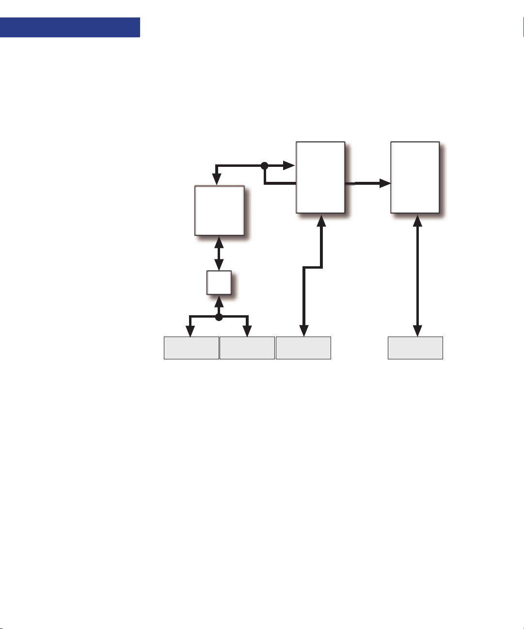
F i g u r e 1 - 1 :
General System Block Diagram
OVERVIEW
Functional Overview
FUNCTIONAL OVERVIEW
. . . . . . . . . . . . . . . . . . . . . . . . . . . . . . . . . . . . . . . . . . . . . . . . . . . .
The following block diagram provides a functional overview for the CC1000dm:
Monarch
PMC Site 2
64-bit PCI-PCI
Bridge
Hot
Swap
Monarch
PMC Site 1
J1
cPCI
ADDITIONAL INFORMATION
. . . . . . . . . . . . . . . . . . . . . . . . . . . . . . . . . . . . . . . . . . . . . . . . . . . .
J2
cPCI
This section lists the CC1000dm hardware’s regulatory certifications and briefly discusses the terminology and notation conventions used in this manual. It also lists general technical references.
Mean time between failures (MTBF) has been calculated at 1,251,602 hours using the
Method I Case 3, Telcordia Issue 1 model at 30
1-2 CC1000dm User’s Manual 10004281-02
J3
cPCI I/O
J5
cPCI I/O
O
C.
Page 15

OVERVIEW
. . . . . . . . . . . . . . . . . . . . . . . . . . . . . . . . . . . . . . . . . . . . . . . . . . . .
Additional Information
. . . . .
Product Certification
T a b l e 1 - 1 :
Regulatory Agency
Compliance
The CC1000dm hardware has been tested to comply with various safety, immunity, and
emissions requirements as specified by the Federal Communications Commission (FCC),
Underwriters Laboratories®, Inc. (UL), and others. The following table summarizes this
compliance:
Type: Specification:
Safety IEC60950/EN60950 — Safety of Information Technology Equipment
(Western Europe)
UL60950-1, CSA C22.2 No. 60950-1-03, 1st Edition — Safety of
Information Technology Equipment, including Electrical Business
Equipment (BI-National)
EMC FCC Part 15, Class A — Title 47, Code of Federal Regulations, Radio
Frequency Devices
ICES 003, Class A — Radiated and Conducted Emissions, Canada
EN55022 — Information Technology Equipment, Radio Disturbance
Characteristics, Limits and Methods of Measurement
EN55024 — Information Technology Equipment, Immunity
Characteristics, Limits and Methods of Measurement
ETSI EN300386 — Electromagnetic Compatibility and Radio Spectrum
Matters (ERM), Telecommunication Network Equipment, Electromagnetic
Compatibility (EMC) Requirements
Artesyn maintains test reports that provide specific information regarding the methods
and equipment used in compliance testing. Unshielded external I/O cables, loose screws,
or a poorly grounded chassis may adversely affect the CC1000dm hardware’s ability to
comply with any of the stated specifications.
The UL web site at ul.com has a list of Artesyn’s UL certifications. To find the list,
search in the online certifications directory using Artesyn’s UL file number, E190079.
There is a list for products distributed in the United States, as well as a list for products
shipped to Canada. To find the CC1000dm, search in the list for 10005129-xx, where xx
changes with each revision of the printed circuit board.
RoHS Compliance
The CC1000dm is compliant with the European Union’s RoHS (Restriction of Use of
Hazardous Substances) directive created to limit harm to the environment and human
health by restricting the use of harmful substances in electrical and electronic equipment. Effective July 1, 2006, RoHS restricts the use of six substances: cadmium (Cd),
mercury (Hg), hexavalent chromium (Cr (VI)), polybrominated biphenyls (PBBs), polybrominated diphenyl ethers (PBDEs) and lead (Pb). Configurations that are 5-of-6 are
built with tin-lead solder per the lead-in-solder RoHS exemption.
10004281-02 CC1000dm User’s Manual 1-3
Page 16

OVERVIEW
. . . . . . . . . . . . . . . . . . . . . . . . . . . . . . . . . . . . . . . . . . . . . . . . . . . .
1
Additional Information
To obtain a certificate of conformity (CoC) for the CC1000dm, send an e-mail to
sales@artesyncp.com or call 1-800-356-9602. Have the part number(s) (e.g.,
C000####-##) for your configuration(s) available when contacting Artesyn.
Terminology and Notation
Active low signals:
Byte, word:
Radix 2 and 16:
Technical References
T a b l e 1 - 2 :
Technical Refe rences
An active low signal is indicated with an asterisk * after the signal name.
Throughout this manual byte refers to 8 bits, word refers to 16 bits, and long word refers
to 32 bits, double long word refers to 64 bits.
PLD:
This manual uses the acronym, PLD, as a generic term for programmable logic device
(also known as FPGA, CPLD, EPLD, etc.).
Hexadecimal numbers end with a subscript 16. Binary numbers are shown with a sub-
script 2.
Further information on basic operation and programming of the CC1000dm components can be found in the following documents:
Device / Interface: Document: 1
Bridge PCI 6254 (HB6) Dual Mode Universal PCI-to-PCI Bridge Data Book
CompactPCI PICMG® 2.0 CompactPCI® Specification/Revision 3.0. October 1, 1999
(PLX Technology, Inc.; Version 2.0 May 2003)
http://www.plxtech.com/
PICMG® 2.1 CompactPCI® Hot Swap Specification/Revision 2.0 January
17, 2001
PICMG® 2.2 VME64x on CompactPCI® Specification/Revision 1.0 August
7, 1998
PICMG® 2.3 PMC on CompactPCI® Specification/Revision 1.0 August 7,
1998
PICMG® 2.4 IP on CompactPCI® Specification/Revision 1.0 August 7,
1998
(PCI Industrial Computer Manufacturers Group, PICMG; Wakefield, MA)
http://www.picmg.org/
1-4 CC1000dm User’s Manual 10004281-02
Page 17

OVERVIEW
. . . . . . . . . . . . . . . . . . . . . . . . . . . . . . . . . . . . . . . . . . . . . . . . . . . .
Additional Information
. . . . .
Device / Interface: Document: 1 (continued)
PMC IEEE Standard for a Common Mezzanine Card Family: CMC IEEE Std
1386-2001 (Institute of Electrical and Electronics Engineers, Inc. (IEEE):
New York, NY)
http://www.ieee.org/
IEEE Standard Physical and Environmental Layers for PCI Mezzanine
Cards (PMC) IEEE Std 1386.1-2001
(IEEE: New York, NY)
http://www.ieee.org/
PCI Local Bus Specification
(PCI Special Interest Group, Revision 2.3 March 29, 2002)
http://www.pcisig.com/home
Processor PMC Standard for Processor PCI Mezzanine Cards, VITA 32 2003 Revision 1.0a, 29 April 2003 Draft
(VITA Standards Organization)
http://www.vita.com/
1. Frequently, the most current information regarding addenda/errata for specific documents may be
found on the corresponding web site.
10004281-02 CC1000dm User’s Manual 1-5
Page 18

OVERVIEW
1
Additional Information
1-6 CC1000dm User’s Manual 10004281-02
Page 19

S
. . . . . . . . . . . . . . . . . . . . . . . . . . . . . . . . . . .
ETUP
. . . . . . . . . . . . . . . . . . . . . . . . . . . . . . . . . . .
his chapter describes the physical layout of the boards, the setup process, and
how to check for proper operation once the boards have been installed. This
T
chapter also includes troubleshooting, service, and warranty information.
ELECTROSTATIC DISCHARGE
. . . . . . . . . . . . . . . . . . . . . . . . . . . . . . . . . . . . . . . . . . . . . . . . . . . .
Before you begin the setup process, please remember that electrostatic discharge (ESD)
can easily damage the components on the CC1000dm hardware. Electronic devices,
especially those with programmable parts, are susceptible to ESD, which can result in
operational failure. Unless you ground yourself properly, static charges can accumulate
in your body and cause ESD damage when you touch the board.
Caution: Use proper static protection and handle CC1000dm boards only when absolutely necessary. Always
wear a wriststrap to ground your body before touching a board. Keep your body grounded while
!
handling the board. Hold the board by its edges—do not touch any components or circuits. When
the board is not in an enclosure, store it in a static-shielding bag.
To ground yourself, wear a grounding wriststrap. Simply placing the board on top of a
static-shielding bag does not provide any protection—place it on a grounded dissipative
mat. Do not place the board on metal or other conductive surfaces.
. . . . .
2
CC1000DM CIRCUIT BOARD
. . . . . . . . . . . . . . . . . . . . . . . . . . . . . . . . . . . . . . . . . . . . . . . . . . . .
The CC1000dm circuit board is a cPCI carrier card assembly. It uses a 12-layer printed
circuit board with the following dimensions:
T a b l e 2 - 1 :
Circuit Board Dimensions
Width: Depth:
9.2 in. (233.35 mm) 6.3 in. (160.00 mm)
10004281-02 CC1000dm User’s Manual 2-1
Page 20
SETUP
2
CC1000dm Circuit Board
The following figures show the front panel, component maps, and jumper locations for
the CC1000dm circuit board.
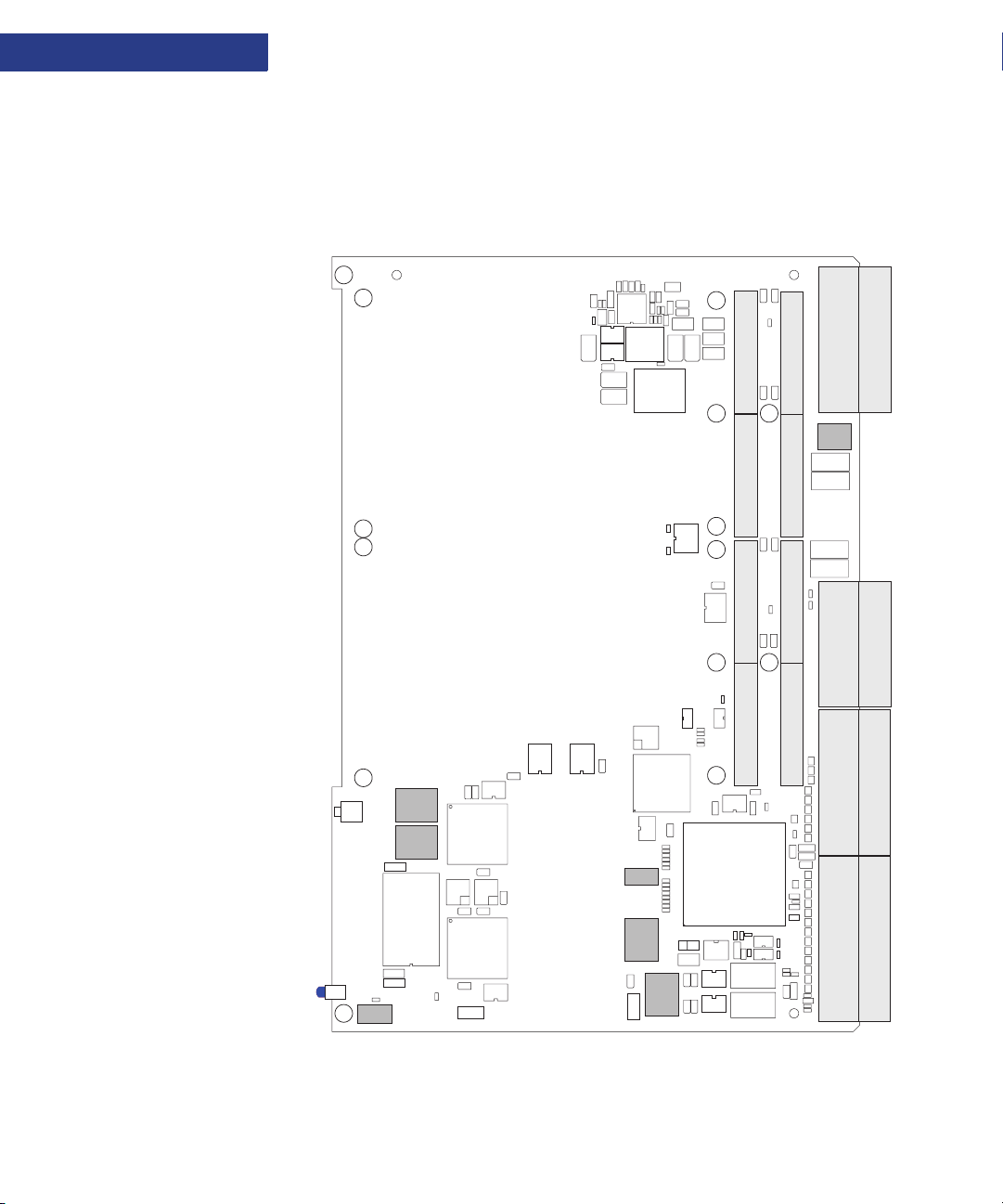
F i g u r e 2 - 1 :
Component Map, Top (rev. 02)
CR1
SW1
C13
R4
C12
R5
C15
CR4
M1
M2
C16
C19
C18
R12
R14
R18
R6
U14
C17
C33
C27
C22
C32
R16
R17
C21
R13
R15
C31
R33
C43
L1
C42
C41
C28
C37
C23
L6
J21
C55
C49
R44
J5
J22
C54
C48
CR5
R8
R7
R11
R10
JP7
F4
J24
F3
U15
C25 C26
C53
C47
F2
F1
C40
J11 J23
U18
C39
U23
U19
R38
J13
R37
Y3
R36
R35
U8
U11
C11
U5
C7
JP2
JP1
C3
U1
C6
U3
C9
Y1
Y2
C10
C5
C8
U2
C2
C1
R1
J6
C4
U4
R2
R3
C14
JP5
JP3
C20
U13
C24
U12
R32
R31
R30
R29
R28
R27
R26
R25
R24
R23
R22
R21
R20
R19
CR6
C36
C30
C35
JP6
C29
R9
C34
U20
C38
U16
PCI 6254
U17
M6
M5
R428
R427
C44
R41
R40
R39
C45
C186
U22
U21
R426
R312
R56
R55
R43
C52
C46
J14 J12
RN24
RN23
RN22
RN21
RN20
RN19
R42
RN18
RN2
RN17
C58
RN16
R54
C57
R53
C63
RN15
RN14
RN1
RN13
R51
C59
RN12
R50
RN11
R49
RN10
RN9
RN8
C51
C50
R46
R45
J1 J2 J3
RN7
RN6
RN5
R48
RN4
RN3
R47
C56
C62
R52
C61
C60
2-2 CC1000dm User’s Manual 10004281-02
Page 21

F i g u r e 2 - 2 :
Component Map, Bottom (rev. 02)
SETUP
CC1000dm Circuit Board
. . . . .
R188
C94
C104
R418
R57
R58
R59
R60
R77
R61
R78
C64
R79
R80
C65
R89
R88
R90
C66
R91
C67
R62
R63
R64
R65
R66
R67
R68
R69
R70
R75
R76
R422
R171
R181
R402
R147
R120
R156
R184
R148
R174
R173
R419
R423C86
R121
C73C71
C81
R122
R123
C68
R124
R125
R126
R118
L2
R96
C88
R114R113
R81
R127
R82
L3
R128
R97
C74
C75
R83
R129
R115
R71
R109
R84
R130
R98
C82
R99
R73
R74
R100
C83
C84
R119
C69
R105
R110
R85
R111
R86
R112
R87
R131
C85
C76C72
R132
C70
R133
R134
R135
R116
L4
R136
R101
R92
R93
R94
R72
R95
C89
R117
R137
L5
C78
C77
R102
C79
C80
C87
R424
R106
R138
R421
R425
R420
R103
R107
R104
R108
F5
R180
R139
R149
C105
R161
R150
C109
C112
C97
C99
C90
R162
R140
R141
R163
R185
R189
C91
R190
R164
R165
C100
C101
R175C95
R191
R172
R166
R177
R183
R176
R182
R151
R157
R152
R142
R167
R143
R153
C102
C110
C98
C92
R154
R144
R158
R145
R155
R146
R168
C93
R187
R169
R170
C103
C111
C96
R178
R192
R159
R179
R193
R160
C114
C106
R197
R417
C107
C113
C108
R194
R195
R196
R198
R199
R202
C115
R203
R204C116
R209
R210
R206
C117
R211
R212
R200
C119
R201C118
R207
M8
C149
R310
C150R311
M9
R301
R302
C125
C127
C122
C132
C128
C126
R228
R222
C121
R229
R230
R231
R232
R233
R234
R235
R236
R237
R253C130
R238
R239
R240
R241
R242
R243
R244
R223
R224
C123
C120R205
R259
R260
R261
R248
R262
R213
R263
R264
R249
R265
R214
R266
R215
R267
C124
R268
R269
R270
R429
R271
R272
R273
R216
R217
R218
R219
R220
R208
R221
U24
R252
R307
R258
R303
R290
C129
R291
R276
R349
R277
R278
R279
R280
R281
C134
R282
R283
C131
C135
R34
R313
R284
R305
R274
R314
R306
R275
C141
R351
R285
R308
C147C148
R309
R286
R357
C140 C139
C142
R292
R293
R294
R295
R296
R297
R287
C136
C182
F6
R396
R397
C172
R398
RN27
C173
RN28
RN29
RN30
RN31
R405
C161C162
R347
R399
R354
RN32
R406
R400
R393R392
RN33
C165
R409
RN34
R140
RN35
C158
RN36
C174
R350
RN37
R355
RN38
R348
C145
RN39
C183
C175
C166
C146
C184
R411
C167
C185
RN40
R412
RN41
C171
C168
RN26
RN42
R401
R186
RN43
R352
RN44
R353
RN45
RN46
RN47
RN48
680-
XXXXXX
00000000-00 D
R413
C151
R135
R136
R298
R299
R300
C163
C137
C133
C143
R288
R289
R137
C138
R318
R319
R320
R321
R358
R359
R322
C154
R254
R225
R246
R226
R250
R251
R227
R255
R247
R256
R360
R323
R361
R257
R324
R362
R325
R363
R326
R364
R327
R365
R328
R366
R329
R367
R330
R368
R331
R369
R332
R370
R333
R371
R334
R372
R335
R373
R336
R374
R337
R375
R338
R376
R339
R377
R340
R378
R379
R380
R381
R382
R383
R341
R384
R385
R342
R386
R387
C144
R388
R389
R343
R344
R390
R391
R345
C157
R346
C177 C176R414
C152
R394
R395
C153
F7
C178R415
F8
R407
C169R403
F10
F9
C179
C155
C164
C180
C160
C156
C181
R404
R408
R416
C170
10004281-02 CC1000dm User’s Manual 2-3
Page 22

SETUP
2
CC1000dm Circuit Board
Identification Numbers
Connectors
P1–P2:
J1:
J2:
J3:
J5:
Before you install the CC1000dm circuit board in a system, you should record the following information:
❐ The board serial number: 680– ______________________________________ .
The board serial number appears on a bar code sticker located on the back of the
board.
❐ The board product identification: ___________________________________ .
This sticker is located near the board serial number.
It is useful to have these numbers available when you contact the Technical Support
department at Artesyn Communication Products.
The CC1000dm circuit board has various connectors (see the figures beginning on
page 2-3), summarized as follows:
These connectors are not installed on the CC1000dm.
This 110-pin connector has keying for 3.3 volt and 5 volt supplies. See Table 4-3 for the
pin assignments.
This 110-pin connector carries the PCI 64-bit extension signals. See Table 4-4 for the pin
assignments.
This is a 95-pin connector that routes the I/O signals for the PMC I/O, serial port, and
USB port. See
Table 4-5 for the pin assignments.
This 110-pin connector is used for PMC I/O. See Table 4-6 for the pin assignments.
J6:
This is a 3-pin header for the Hot Swap switch.
J11:
This connector shares the 32-bit PCI signals with the J12 connector (secondary bus). In
addition, J11 supports a V(I/O) power supply for universal PCI signaling. It uses 3.3 volt
PCI buffers with a 5 volt tolerance. See
J12:
This connector shares the 32-bit PCI signals with the J11 connector (secondary bus). It
also carries the 3.3 volt supply voltage. See
J13:
This connector carries the 64-bit PCI extensions (secondary bus). See Table 3-9 for the pin
assignments.
J14:
This connector is for user I/O, which routes to J3. See Table 3-9 for the pin assignments.
J21:
This connector shares the 32-bit PCI signals with the J22 connector (secondary bus). In
addition, J21 supports a V(I/O) power supply for universal PCI signaling. It uses 3.3 volt
PCI buffers with a 5 volt tolerance. See
J22:
This connector shares the 32-bit PCI signals with the J21 connector (secondary bus). It
also carries the 3.3 volt supply. See
2-4 CC1000dm User’s Manual 10004281-02
Table 3-9 for the pin assignments.
Table 3-9 for the pin assignments.
Table 3-10 for the pin assignments.
Table 3-10 for the pin assignments.
Page 23

CC1000dm Circuit Board
J23:
This carries the 64-bit PCI extensions (secondary bus). See Table 3-10 for the pin assignments.
J24:
This connector is for user I/O, which routes to J5. See Table 3-10 for the pin assignments.
SETUP
. . . . .
Fuses and Jumpers
F1-F4:
N o t e :
Fuses F5 through F10 are
located on the bottom side,
see Fig. 2-2.
JP1, JP2:
The CC1000dm has various jumpers, headers, and fuses. Please refer to Fig. 2-3 on the
following page for the jumper/header locations.
These are spare fuses on the top side of CC1000dm.
F5:
This fuse (.75 amp) provides protection for the 3.3 volt supply to the PMC JTAG header.
F6:
This fuse (.75 amp) provides protection for the PLD JTAG header.
F7:
This fuse (.75 amp) provides protection for the 5 volt supply to the backplane.
F8:
This fuse (.75 amp) provides protection for the 3.3 volt supply to the backplane.
F9:
This fuse (.75 amp) provides protection for the +12 volt supply to the backplane.
F10:
This fuse (.75 amp) provides protection for the -12 volt supply to the backplane.
Each PMC slot has an associated 10-pin debug header (see Table 3-8).
JP3:
This 10-pin jumper selects the following configurations: local VIO, Monarch, auto
memory, oncard oscillator and bridge serial ROM (see page 2 -7).
JP5:
This 4-pin jumper selects the mode: transparent, non-transparent, legacy (Artesyn
CC1000), or no system controller (see page 2 -9).
JP6:
The programmable logic device (PLD) uses this 10-pin JTAG header (see page 2-9).
JP7:
This is a spare header.
10004281-02 CC1000dm User’s Manual 2-5
Page 24

2
F i g u r e 2 - 3 :
Jumper/Header Locations, Top
View
SETUP
CC1000dm Circuit Board
SW1
CR1
PMC2 JTAG Header
1
9
JP2
2
10
PMC1 JTAG Header
9
1
JP1
10
2
Hot Swap Header
J6
PMC2
PMC1
Mode Select
43
JP5
2
1
Multiple Options Select
9
10
JP3
2
1
JTAG Header
9
10
JP6
2
1
J21
J22
J5
JP7
Spare
J23
J24
F3 F4F2F1
J11
J12
J3J2J1
J13
J14
Reset Switch
The CC1000dm has a push button switch (SW1) on the front panel to reset the secondary PCI bus and inform the CompactPCI bus of the need for enumeration.
2-6 CC1000dm User’s Manual 10004281-02
Page 25

SETUP
CC1000dm Setup
. . . . .
LEDs
F i g u r e 2 - 4 :
Front Panel
All CC1000dm carrier cards have a blue LED which indicates the Hot Swap status, as
shown in
vated by the card ejector handle. The micro-switch indicates to the PCI bridge when the
ejector is open or closed.
CC1000DM SETUP
. . . . . . . . . . . . . . . . . . . . . . . . . . . . . . . . . . . . . . . . . . . . . . . . . . . .
You will need the jumper settings and the PCI signaling in order to set up and check the
operation of the Artesyn CC1000dm carrier card. See
the CC1000dm.
Save the antistatic bag and box for future shipping or storage.
Multiple Option Selection (JP3)
LOCAL VIO SELECTION
The secondary (PMC) side of the PCI bridge can be set for either 3.3 volt or 5 volt signaling. Installing the jumper in JP3 pins 1-2, selects 3.3 volt signaling (default). The
primary (cPCI) side is set externally to the CC1000dm.
Fig. 2-4. The PCI bridge component monitors the micro-switch which is acti-
Fig. 2-3 for the jumper locations on
Caution: Incorrect installation of this jumper can damage PMC modules that only support 3.3 volt signaling.
!
MONARCH SELECTION
The PMC slots can be configured to support either Monarch or non-Monarch modules.
Setting the jumper to select PMC1 Monarch configures the board for a Monarch module
in PMC Slot 1 (factory default). Without a jumper installed in JP3 pins 3-4, this configures the board for a Monarch in PMC slot 2. Please refer to page 3 -2 for further details
regarding Monarch functionality.
AUTO MEMORY SELECTION
In non-transparent mode, the cross bridge memory (XB_MEM) setting allows the primary side to enumerate the primary bus with a default 16-megabyte window. Otherwise
the primary side may experience a delay in enumeration if the secondary side PMC has
a long enumeration time.
10004281-02 CC1000dm User’s Manual 2-7
Page 26

2
. . . . . . . . . . . . . . . . . . . . . . . . . . . . . . . . . . . . . . . . . . . . . . . . . . .
F i g u r e 2 - 5 :
Multipl e Option Jumper, JP3
SETUP
CC1000dm Setup
If the Serial ROM (SROM) is enabled, it overrides the 16-megabyte window with the
applicable window. Install this jumper when using the SROM and also when the S-Port
ready and P-Port ready bits are to be set. This allows the bridge to be enumerated without any further interaction.
OSCILLATOR SELECTION
When the 66 MHz oncard oscillator is enabled, this allows the CC1000dm to produce its
own 33/66 MHz clock for the secondary side. This is independent of the primary frequency.
BRIDGE SERIAL ROM SELECTION
Installing the bridge SROM jumper disables the PCI 6254 bridge SROM. The EEPROM is
used to initialize the registers. If the EEPROM becomes corrupted and locks the system,
disabling the EEPROM allows default access to the CC1000dm.
12
Local VIO
T a b l e 2 - 2 :
Multipl e Option Jumper
Selection, JP3
Monarch
43
65
XB_MEM
78
910
Signal Name: Bit: Selection: Jumper:
VIO_SEL_3_3V*
PMC_Mon_SEL_1*
XB_MEM_SEL*
EXT_OSC*
Oscillator
Bridge EEPROM
0 3.3 V Local VIO (default) Install 1-2
1 5 V Local VIO Remove 1-2
0 PMC slot 1 (PMC1) is Monarch (default) Install 3-4
1 PMC slot 2 (PMC2) is Monarch Remove 3-4
0 Auto (cross bridge) memory window in non-
transparent mode enabled (default)
1 Auto (cross bridge) memory window in non-
transparent mode disabled
0 On-board 66 MHz oscillator enabled Install 7-8
1 On-board 66 MHz oscillator disabled (default) Remove 7-8
Install 5-6
Remove 5-6
2-8 CC1000dm User’s Manual 10004281-02
Page 27

SETUP
. . . . . . . . . . . . . . . . . . . . . . . . . . . . . . . . . . . . . . .
. . . . . . . . . . . . . . . . . . . . . . . . . . . . . . .
. . . . . . . . . . . . . . . . . . . . . . . . . . . . . . . . . . . . . . . . . . . . . . . . . . .
CC1000dm Setup
. . . . .
Mode Selection (JP5)
T a b l e 2 - 3 :
System Controller Modes,
JP5
PLD Header (JP6)
F i g u r e 2 - 6 :
PLD Header, JP6
Signal Name: Bit: Selection: (continued) Jumper:
0 Bridge serial ROM enabled (default) Remove 9-10
BRIDGE_SEE_EN*
1 Bridge serial ROM disabled Install 9-10
The system controller modes are selected by jumper JP5. The legacy product is the Artesyn CC1000 carrier card.
Jumper Position: Mode_Sel (3:0): Mode:
1-2 1000 Non-Transparent (default)
3-4 1011 Transparent
2-4 0001 Legacy (CC1000)
None 1001 No System Controller
This 10-pin JTAG header is used by the PLD.
10
2
9
1
T a b l e 2 - 4 :
PLD Header Pin Assignments,
JP6
Pin: Signal: Pin: Signal:
1 PLD_TCK 2 ground
3PLD_TDO 4PLD_3_3V
5PLD_TMS
7 no connect 8 no connect
9 PLD_TDI 10 ground
6 no connect
10004281-02 CC1000dm User’s Manual 2-9
Page 28

SETUP
. . . . . . . . . . . . . . . . . . . . . . . . . . . . . . . . . . . . . . . . . . . .
. . . . . . . . . . . . . . . . . . . . . . . . . . . . . . . . . . . . . .
2
Operational Checks
Power Requirements
T a b l e 2 - 5 :
Power Requirements
Be sure your power supply is sufficient for the board. The combined power (3.3 volts
and 5 volts) for a CC1000dm is 27 watts.
for the CC1000dm. Please contact Artesyn Technical Support at 1http://www.artesyncp.com/support on the internet or send E-mail to support@artesyncp.com if you
have specific questions regarding the board’s power requirements.
Voltage: Range:
+3.3 V +5/-3% 1.0 Board logic
+5 V +5/-3% 0.4 Board logic
+12 V ±5% 0.5 PMC slot power
–12 V ±5% 0.5 PMC slot power
VIO ±5% 0.75 PCI signaling for board logic
Environmental Considerations
As with any printed circuit board, be sure that air flow to the board is adequate. Chassis
constraints and other factors greatly affect the air flow rate. The environmental requirements are as follows:.
T a b l e 2 - 6 :
Environmental Requirements
Voltage: Usage:
Operating Temperature 0 to +55O Centigrade, ambient (at board)
Table 2-5 lists the specific power requirements
Typical Current
(amps): Usage:
Relative Humidity Not to exceed 95% (non-condensing)
Storage Temperature -40 to +85
Shock and Vibration NEBS Level 3 compliant
OPERATIONAL CHECKS
. . . . . . . . . . . . . . . . . . . . . . . . . . . . . . . . . . . . . . . . . . . . . . . . . . . .
All products are tested before they are shipped from the factory. When you receive your
CC1000dm, follow these steps to assure yourself that the system is operational:
1 Visually inspect the board for components that could have loosened during shipment.
2 Verify that the front panel is secure.
3 By default, the CC1000dm carrier card is configured to support 3.3 V I/O operation on the
secondary bus. Please be sure to select the appropriate voltage for your application.
2-10 CC1000dm User’s Manual 10004281-02
O
Centigrade, ambient
Page 29

F i g u r e 2 - 7 :
Basic Reset Diagram
SETUP
Reset Methods
. . . . .
RESET METHODS
. . . . . . . . . . . . . . . . . . . . . . . . . . . . . . . . . . . . . . . . . . . . . . . . . . . .
Fig. 2-7 shows the basic reset diagram for the CC1000dm. For PLD signal routing changes
for each of the four modes, see
Fig. 2-8.
PCI_VIO
5.11 K 5.11 K
PMC Slots (2)
10 K
PMC_RSTOUT*
PCI_EREADY*
PCI_VIO
CONN_CPCI_RST
cPCI
CONN_CPCI_BD_SEL*
Backside
Voltage
Monitor and
PB Reset
Early Power
Voltage
Monitor
10
CPCI_RST*
BACKSIDE_PWR_GD
BACKSIDE_PWR_RST*
EP_BAD_RST*
EP_PWRGD
0
HS_FAULT*
PLD
HS_ON*
HS_PWRGD*
Hot Swap Controller
BRIDGE_RST*
BRIDGE_RST_OUT*
S_RSTIN*
S_RSTOUT*
PCI 6254
Bridge
10004281-02 CC1000dm User’s Manual 2-11
Page 30

SETUP
2
Reset Methods
F i g u r e 2 - 8 :
PLD Signal Routing–All Modes
Non-transparent
PCI_VIO
10 K
5.11 K
PMC_RSTOUT*
CONN_CPCI_RST
CONN_CPCI_BD_SEL*
10
BACKSIDE_PWR_GD
BACKSIDE_PWR_RST*
CPCI_RST*
PCIXCAP_HEALTHY*
(internal signal)
PLD
BRIDGE_RST_OUT*
HS_ON*
HS_PWRGD*
BRIDGE_RST*
S_RSTIN*
S_RSTOUT*
CONN_CPCI_RST
CONN_CPCI_BD_SEL*
Legacy
PCI_VIO
10 K
5.11 K
PMC_RSTOUT*
PLD
CONN_CPCI_RST
CONN_CPCI_BD_SEL*
10
BACKSIDE_PWR_GD
BACKSIDE_PWR_RST*
CPCI_RST*
BRIDGE_RST_OUT*
HS_ON*
HS_PWRGD*
BRIDGE_RST*
S_RSTIN*
S_RSTOUT*
CONN_CPCI_RST
CONN_CPCI_BD_SEL*
Any of the following methods reset the entire board:
10
CPCI_RST*
BACKSIDE_PWR_GD
BACKSIDE_PWR_RST*
10
CPCI_RST*
BACKSIDE_PWR_GD
BACKSIDE_PWR_RST*
Transparent
PCI_VIO
10 K
5.11 K
PMC_RSTOUT*
PCIXCAP_HEALTHY*
PLD
(internal signal)
(1)
HS_ON*
HS_PWRGD*
No System Controller
PCI_VIO
10 K
5.11 K
PMC_RSTOUT*
PLD
(0)
HS_ON*
HS_PWRGD*
BRIDGE_RST*
BRIDGE_RST_OUT*
S_RSTIN*
S_RSTOUT*
BRIDGE_RST*
BRIDGE_RST_OUT*
S_RSTIN*
S_RSTOUT*
• At power-up, the CC1000dm carrier card generates a hard reset.
• The voltage monitor detects voltage supplies of +5 V, +3.3 V, +12 V,-12 V, or
PMC_3_3V that fall below the minimum thresholds of +4.7 V, +3.1 V,
+11.4 V, -10.8 V, or 3.1 V, respectively.
• Input from the cPCI reset signal (except when in the no system controller mode)
• Pressing the reset switch (SW1) on the CC1000dm front panel
• Writing to the PLX PCI 6254 (HB6) Bridge Control register from the PCI address
space can generate a reset on the S-RST* signal.
• Input from the RSTOUT* signal from either PMC slot 1 or PMC slot 2.
2-12 CC1000dm User’s Manual 10004281-02
Page 31

SETUP
Troubleshooting
. . . . .
TROUBLESHOOTING
. . . . . . . . . . . . . . . . . . . . . . . . . . . . . . . . . . . . . . . . . . . . . . . . . . . .
In case of difficulty, use this checklist:
❐ Be sure the CC1000dm circuit board is seated firmly in the card cage.
❐ Be sure the system is not overheating.
❐ Check the cables and connectors to be certain they are secure.
❐ Verify that the PMC modules are fully installed and seated firmly in the PMC slots.
Technical Support
Service Information
If you need help resolving a problem with your CC1000dm, visit
http://www.artesyncp.com/support on the internet or send E-mail to
support@artesyncp.com. Please have the following information handy:
• CC1000dm serial number and product identification from the sticker
• version and part number of the operating system (if applicable)
• whether your board has been customized for options
• license agreements (if applicable)
If you do not have internet access, please call Artesyn at (800) 327-1251 for further
assistance.
If you plan to return the board to Artesyn Communication Products for service, visit
http://www.artesyncp.com/support on the internet or send E-mail to
serviceinfo@artesyncp.com to obtain a Return Merchandise Authorization (RMA) number. We will ask you to list which items you are returning and the board serial number,
plus your purchase order number and billing information if your CC1000dm hardware
is out of warranty. Contact our Test Services Department for any warranty questions. If
you return the board, be sure to enclose it in an antistatic bag, such as the one in which
it was originally shipped. Send it prepaid to:
Artesyn Communication Products
Test Services Department
8310 Excelsior Drive
Madison, WI 53717
RMA #____________
Please put the RMA number on the outside of the package so we can handle your problem efficiently. Our service department cannot accept material received without an
RMA number.
10004281-02 CC1000dm User’s Manual 2-13
Page 32

SETUP
2
Troubleshooting
2-14 CC1000dm User’s Manual 10004281-02
Page 33

PMC/PCI I
NTERFACE
. . . . . . . . . . . . . . . . . . . . . . . . . . . . . . . . . . .
he CC1000dm has two 3.3 volt/5 volt, 64-bit, Processor PMC slots, designated
PMC1 and PMC2. Either slot can be configured as a Monarch module by means
T
of a ten-pin jumper (see JP3 on page 2 -7). When the CC1000dm is in transpar-
ent mode, neither PMC slot is selected as Monarch. The PMC slots comply with IEEE
Standard for a Common Mezzanine Card Family: CMC IEEE Std 1386-2001.
PCI BRIDGE FEATURES
. . . . . . . . . . . . . . . . . . . . . . . . . . . . . . . . . . . . . . . . . . . . . . . . . . . .
The CC1000dm supports PCI bus speeds of up to 66 MHz with the PLX PCI 6254 (HB6)
dual-mode (transparent and non-transparent), universal 64-bit PCI-to-PCI bridge. In
transparent mode, the PCI bus is connected to the primary port. In non-transparent
mode, the PCI bus is connected to the secondary port. Some additional features include:
• The PLX PCI 6254 bridge complies with the PCI Local Bus Specification Revision 2.3
Bus Interface
• 64-bit PCI address/data busses
• Asynchronous primary and secondary ports can operate at different frequencies–a
maximum ratio of 1:2:5 or 2:5:1 between primary and secondary bus clocks
. . . . .
3
• Serial ROM interface
•PCI bus arbiter
PMC MODULE INSTALLATION
. . . . . . . . . . . . . . . . . . . . . . . . . . . . . . . . . . . . . . . . . . . . . . . . . . . .
The CC1000dm carrier card has two PMC expansion slots–J1x and J2x (PMC1 and
PMC2). A single-width PMC module may be installed at each of these slots. Each slot
includes a cutout on the front panel for I/O.
When installing a PMC module, follow these guidelines:
1 Before adding modules to the CC1000dm carrier card, be sure that the combined power
requirements of the CC1000dm carrier card and the PMC modules do not exceed the system’s power
supply rating or cPCI ratings. Table 3-1 . describes the power available at the PMC slots.
10004281-02 CC1000dm User’s Manual 3-1
Page 34

3
. . . . . . . . . . . . . . . . . . . . . . . . . . . . . . . . . . . .
. . . . . . . . . . . . . . . . . . . . . . . . . . . . . . .
T a b l e 3 - 1 :
PMC Slots Available Power
N o t e :
A maximum load current of 6
amps (worst case) results in a
voltage drop of approximately
100 mV to the PMC 5 volt
power supply inputs. To ensure
proper module operation,
adjust the CompactPCI power
supply to accommodate any
voltage drop or power supply
ripple that may occur when
operating the ca rrier card.
PMC/PCI INTERFACE
PMC Module Installation
3.3 Volts: 5 Volts: 3.3 and 5 Volts Combined:
8.5 amps 6 amps 28-30 watts
2 To prevent ESD damage to the CC1000dm carrier card and the PMC modules, wear a grounding
wriststrap and use a grounded work surface while handling the card.
3 Set up the PMC module and install it on the CC1000dm carrier card as specified in the module’s
hardware manual.
Monarch Functionality
Device Mapping
T a b l e 3 - 2 :
IDSEL Mapping for PCI
Devices
Each slot (PMC1 and PMC2) on the CC1000dm carrier card can be configured to function as either a Monarch or non-Monarch PMC slot (in non-transparency or legacy
mode), as described in the Processor PMC Standard for Processor PCI Mezzanine Cards,
VITA 32- 2003 Specification. Although only one slot can be a Monarch, there can be
as many non-Monarch PMCs as the carrier card can support. A module placed on the
Monarch slot performs local PCI bus enumeration and handles PMC interrupts. A module placed on the non-Monarch slot behaves in the traditional slave processor manner.
Both slots have the ability to be configured as either Monarch or non-Monarch by the
10-pin jumper at JP3.
Once the Monarch PMC module has completed initialization of the CC1000dm local
bus, the PCI agents located on that bus are available for access. There are up to two PCI
devices installed on the PLX PCI 6254 (HB6) secondary bus and two PCI IDSEL lines
allocated to each PMC slot.
PCI Address Line: Local PCI Device IDSEL Connection:
AD22 PMC 1
AD21 PMC 1 Alternate Device
AD20 PMC 2
AD19 PMC 2 Alternate Device
AD18 PLX PCI 6254 (HB6) PCI Bridge
Table 3-2 lists all the IDSEL mappings.
3-2 CC1000dm User’s Manual 10004281-02
Page 35

PMC/PCI INTERFACE
. . . . . . . . . . . . . . . . . . . . . . . . . . . . . . . . . . . . . . . . . . . . . . . . . . . .
. . . . . . . . . . . . . . . . . . . . . . . . . . . . . . . . . . . . . . . . . . . . . . . . . . . .
PMC Module Installation
. . . . .
Timing
Interrupts
T a b l e 3 - 3 :
PMCx Interrupt Mapping
The module interface transfers data between the PCI and local memory at burst data
rates. When two modules are installed, they both contend for ownership of a common
bus, which may reduce the individual performance of each module. Specific transfer
rates to the PCI bus are dependent on the module design.
Many PMC modules also incorporate a bridge chip between their PCI and local busses,
essentially creating two bridges that must be crossed to complete a cycle. Often, the
second bridge is a source of long delays due to the associated bus acquisition latency.
Initialization and time-out values should be set up to accommodate any additional
latency.
External interrupts that are controlled by the CC1000dm carrier card are routed to the
on-board devices/slots as follows:
PMC1/ PMC2
Base PCI
Interrupt
Assignment (secondary):
INTA INTA (J21, pin 4) INTC (J11, pin 6)
INTB INTB (J21, pin 5) INTD (J11, pin 9)
INTC PLX PCI 6254 (HB6) INTC (J21, pin 6) INTA (J11, pin 4)
INTD INTD (J21, pin 9) INTB (J11, pin 5)
(Transparent, non-transparent, no
system controller modes)
System Controller PCI Interrupt Line:
PMC1
(Legacy mode only)
Non-System Controller
PCI Interrupt Line:
T a b l e 3 - 4 :
cPCI Interrupt Mapping
Arbitration
Base cPCI Interrupt
Assignment:
INTA (J1, pin A3) INTA INTA (PCI 6254 primary side)
INTB (J1, pin B3) INTB –
INTC (J1, pin C3) INTC –
INTD (J1, pin E3) INTD –
The CC1000dm arbitration control for the on-board PCI devices is provided by the PLX
PCI 6254 PCI-to-PCI bridge. The PCI 6254 arbitrates for use of the primary bus when
initiating upstream transactions and for use of the secondary bus when forwarding
downstream transactions. The primary bus arbiter is external to the PCI 6254, and the
secondary bus is an internal arbiter on the PCI 6254.
Transparent Mode
(secondary): Non-Transparent or Legacy Mode:
10004281-02 CC1000dm User’s Manual 3-3
Page 36

PMC/PCI INTERFACE
3
PMC Module Installation
R e g i s t e r 3 - 1 :
Intern al Arbiter Control Register
151413121110987654 3 210
BPC HPMHP HPMLP HPGAHPGFLPGALPG
The Internal Arbiter Control register is located at offset 50h. All bits are read/write.
LPGF:
Low Priority Group Fixed arbitration
F
1 Uses the fixed priority arbitration scheme
0 Uses the rotating priority arbitration scheme (default)
LPGA:
Low Priority Group Arbitration order
This bit is only valid when the low priority arbitration group is set to a fixed arbitration
scheme (relative to HPM).
1 Priority decreases in ascending numbers of the master
0 Priority increases in ascending numbers of the master (default)
HPGF:
High Priority Group Fixed arbitration
1 Uses the fixed priority arbitration scheme
0 Uses the rotating priority arbitration scheme (default)
HPGA:
High Priority Group Arbitration order
This bit is only valid when the high priority arbitration group is set to a fixed arbitration scheme (relative to HPM).
1 Priority decreases in ascending numbers of the master
0 Priority increases in ascending numbers of the master (default)
HPMLP:
Highest Priority Master in Low Priority group
This controls which master in the low priority group has the highest priority (only for
fixed arbitration scheme).
0000 Master#0 has highest priority (default)
0001 Master#1 has highest priority
to…
1001 PCI 6254 has highest priority
1010- 1111 r es er v ed
HPMHP:
Highest Priority Master in High Priority group
This controls which master in the high priority group has the highest priority. It is valid
only in the fixed arbitration scheme.
0000 Master#0 has highest priority (default)
0001 Master#1 has highest priority
3-4 CC1000dm User’s Manual 10004281-02
Page 37

. . . . . . . . . . . . . . . . . . . . . . . . . .
T a b l e 3 - 5 :
Request/Grant Assignments
PMC/PCI INTERFACE
PMC Module Installation
to…
1001 PCI 6254 has highest priority
1010- 1111 r es er v ed
BPC:
Bus Parking Control
This controls the bus grant behavior during idle.
0000 Last master granted is parked (default)
0001 Master #0 is parked
to…
1001 Mas te r #8 is parked
1010 PCI 6254 is parked
Others Grant is deasserted
The secondary arbiter implements a programmable two-level rotating algorithm
whereby the priorities are re-evaluated at the start of each new transaction on the secondary PCI bus. From this point until the time the next transactions starts, the arbiter
will assert grants corresponding to the highest priority request asserted. The arbiter supports up to ten request/grant pairs. The request/grant assignments for the arbiter are
shown in the following table. For more detailed information regarding arbitration, refer
to the PLX PCI 6254 documentation listed in the Technical References
CC1000dm
Request/Grant Local PCI Bus Device:
Table 1-2.
0PMC 1
. . . . .
1PMC 2
2 reserved
3 reserved
4 PMC 1 Alternate Device
5 PMC 2 Alternate Device
6 reserved
7 reserved
8 reserved
9 PCI 6254
10004281-02 CC1000dm User’s Manual 3-5
Page 38

. . . . . . . . . . . . . . . . . . . . . . . . . . . . . . . . . . . . . . . . . . . . . . . . . . . .
T a b l e 3 - 6 :
PLX PCI 6254 Configuration
Signals
PMC/PCI INTERFACE
3
Bridge EEPROM
BRIDGE EEPROM
. . . . . . . . . . . . . . . . . . . . . . . . . . . . . . . . . . . . . . . . . . . . . . . . . . . .
The PLX PCI 6254 PCI-to-PCI bridge utilizes ROM interface signals to initialize the PCI
6254 registers. The following table briefly describes these signals (see the data book for
complete information):
Signal Description:
EEPCLK The EEPROM Clock output signal to the EEPROM interface is used during
autoload and for VPD functions. This pin is tri-stated if EE_EN* = 1.
EEPDATA The EEPROM Serial Data interfaces to the EEPROM (bi-directional). This pin
EE_EN* The EEPROM Enable LOW input enables EEPROM access.
is tri-stated if EE_EN* = 1.
0=enable EEPROM use
1=connect to logic 1 state
PCI 6254 CONFIGURATION REGISTERS
. . . . . . . . . . . . . . . . . . . . . . . . . . . . . . . . . . . . . . . . . . . . . . . . . . . .
The PCI 6254 can be configured to act as either a transparent or non-transparent PCIto-PCI bridge by selecting the appropriate jumper on JP5 (see page 2-9). In transparent
R e g i s t e r 3 - 2 :
PCI6254 Configuration Registers–
Transparent Mode
Primary
Offset 31 24 23 16 15 8 7 0
00h Device ID Vendor ID
04h Primary Status Primary Command
08h Class Code Revision ID
0Ch BIST Header Type Primary Latency Time Cache Line Size
10h
18h Secondary Latency Timer
mode, the CC1000dm system PCI bus is connected to the PCI 6254 primary port. The
PCI 6254 non-transparent mode acts as a memory-mapped PCI device with the primary
port connected to the cPCI backplane.
reserved
Subordinate Bus Number Secondary Bus Number Primary Bus Number
1Ch
20h
24h
3-6 CC1000dm User’s Manual 10004281-02
Secondary Status I/O Limit I/O Base
Memory Limit Memory Base
Prefetchable Memory Limit Prefetchable Memory Base
Page 39

PMC/PCI INTERFACE
PCI 6254 Configuration Registers
. . . . .
28h
2Ch
30h
34h
38h
3Ch
40h
44h
48h
4Ch
50h
54h EEPROM Data EEPROM Address EEPROM Control
58h
Secondary Incremental
Prefetch Count
I/O Limit Upper 16 Bits I/O Base Upper 16 Bits
Bridge Control Interrupt Pin
Arbiter Control Diagnostic Control Chip Control
Miscellaneous Options Time-out Control
reserved
reserved Test Register Internal Arbiter Control
Prefetchable Memory Base Upper 32 Bits
Prefetchable Memory Limit Upper 32 Bits
reserved
reserved
Primary Incremental
Prefetch Count
Secondary Flow Through
Control
reserved
Secondary Prefetch Line
Count
Secondary Maximum
Prefetch Count
ECP Pointer
reserved
Primary Flow Through
Control
Primary Prefetch Line
Count
Primary Maximum Prefetch
Count
64h GPIO[3-0] Input Data
68h Clkrun Register P_SERR* Status Clock Control
6Ch Private Memory Li mit Private Memory Base
70h Private Memory Base Upper 32 Bits
74h Private Memory Limit Upper 32 Bits
78h
9Ch GPIO[7-4] Input Dataport GPIO[7-4] Output Enable GPIO[7-4] Output Data
A0h GPIO[15-8] Input Dataport GPIO[15-8] Output Enable GPIO[15-8] Output Data Power-up Status
GPIO[3-0] Output Enable
Control
10004281-02 CC1000dm User’s Manual 3-7
GPIO[3-0] Output Data P_SERR* Event Disable
reserved
Hot Swap Switch ROR
Control
Page 40

PMC/PCI INTERFACE
3
PCI 6254 Configuration Registers
ACh reserved
D0h Extended Register Index
reserved reserved reserved
D4h Extended Registers Dataport
D8h
reserved
DCh Power Management Capabilities Next Item Pointer=E4 Capability ID=01
E0h Power Management Data PMCSR Bridge Support Power Management CSR
E4h
reserved HSCSR=00 Next Item Pointer=E8 Capability ID=06
E8h VPD Register=0000 Next Item Pointer=00 Capability ID=03
ECh VPD Data Register=0000_0000
F0h
reserved
R e g i s t e r 3 - 3 :
PCI6254 Configuration Registers–
Non-Transparent Mode
Primary
31 24 23 16 15 8 7 0
Offset
00h Device ID Vendor ID
04h Primary Status Primary Command
08h Class Code Revision ID
0Ch BIST Header Type Primary Latency Time Primary Cache Line Size
10h Downstream I/O or Memory 0 Bar
14h Downstream Memory 1 Bar
18h Downstream Memory 2 Bar or Downstream Memory 1 Bar Upper 32 bits
1Ch
reserved
2Ch Subsystem ID Subsystem Vendor ID
30h
34h
3-8 CC1000dm User’s Manual 10004281-02
reserved Capability Pointer
reserved
Page 41

PMC/PCI INTERFACE
PCI 6254 Configuration Registers
38h reserved
3Ch Primary Maximum Latency Primary Minimum Grant Primary Interrupt Pin Primary Interrupt Line
40h Device ID Vendor ID
44h Secondary Status Secondary Command
48h Class Code Revision ID
4Ch BIST Header Type Secondary Latency Timer Secondary Cache Line Size
50h Upstream I/O or Memory 0 Bar
54h Upstream Memory 1 Bar
58h Upstream Memory 2 Bar or Upstream Memory 1 Bar Upper 32 bits
. . . . .
5Ch
6Ch Subsystem ID Subsystem Vendor ID
70h
74h
78h
7Ch Secondary Max Latency Secondary Minimum Grant Secondary Interrupt Pin Secondary Interrupt Line
80h XB Downstream Configuration Address
84h XB Downstream Configuration Dataport
88h XB Upstream Configuration Address
8Ch XB Upstream Configuration Dataport
90h
94h
98h GPIO[3-0] Input Data
reserved
reserved SERR* Event Disable Clock Control
reserved Capability Pointer
XB Config Access
Semaphore Status
GPIO[3-0] Output Enable
Control
reserved
reserved
reserved
XB Upstream Config Own
Semaphore
GPIO[3-0] Output Data SERR* Status
XB Downstream Config
Own Semaphore
10004281-02 CC1000dm User’s Manual 3-9
Page 42

PMC/PCI INTERFACE
3
PCI 6254 Configuration Registers
9Ch GPIO[7-4] Input Register GPIO[7-4] Output Enable GPIO[7-4] Output Data
A0h GPIO[15-8] Input Register GPIO[15-8] Output Enable GPIO[15-8] Output Data Power-up Status
A4h Upstream Message 3 Upstream Message 2 Upstream Message 1 Upstream Message 0
A8h Downstream Message 3 Downstream Message 2 Downstream Message 1 Downstream Message 0
ACh MSI Control Next Item Pointer=00 MSI Cap ID=5 (rev AA=8)
B0h MSI Address
B4h MSI U pper Address
B8h
BCh
C0h Downstream Doorbell Request Downstream Doorbell Enable
C4h Upstream Doorbell Request Upstream Doorbell Enable
C8h Upstream Interrupt Enable
CCh
Downstream Interrupt
Enable
reserved MSI Data
reserved
Downstream Interrupt
Status
Upstream Interrupt Status Upstream Doorbell Status
Downstream Doorbell Status
Hot Swap Switch ROR
Control
D0h Extended Register Index NT Config Own Semaphore
D4h Extended Registers Dataport
D8h Arbiter Control Diagnostic Control Chip Control
DCh Power Management Capabilities Next Item Pointer=E4 Capability ID=01
E0h Power Management Data PMSCSR Bridge Support Power Management CSR
E4h
E8h VPD Register=0000 Next Item Pointer=00 Capability ID=03
ECh VPD Data Register=0000_0000
F0h
3-10 CC1000dm User’s Manual 10004281-02
reserved HSCSR=00 Next Item Pointer=E8 Capability ID=06
reserved
reserved reserved
Page 43

PMC/PCI INTERFACE
. . . . . . . . . . . . . . . . . . . . . . . . . . . . . . . . . . . . . . . . . . . . . . . . .
. . . . . . . . . . . . . . . . . . . . . . . . . . . . .
PCI Identification Values
. . . . .
PCI IDENTIFICATION VALUES
. . . . . . . . . . . . . . . . . . . . . . . . . . . . . . . . . . . . . . . . . . . . . . . . . . . .
Each CC1000dm configuration has a unique set of identification values. The base
address for these values is determined by the CC1000dm’s location in the cPCI rack and
the baseboard. The standard PCI hex offsets are:
T a b l e 3 - 7 :
PCI Identification Values
T a b l e 3 - 8 :
Debug Header Pin
Assignments (JP1, JP2)
Vendor ID 00
Device ID 02
Subsystem Vendor ID 2C
Subsystem ID 2E
All of these values are two bytes wide (half-word). Please refer to the PLX PCI 6254
data book for more information. The following table lists the identification values for
the different CC1000dm configurations:
Vendor
ID (hex):
3388 20 – – Transparent
Device
ID (hex):
21 1223 3A Non-transparent
Subsystem
Vendor ID (hex):
16
16
16
16
Subsystem
Device ID (hex): PCI 6254 Bridge Mode:
JTAG HEADERS
. . . . . . . . . . . . . . . . . . . . . . . . . . . . . . . . . . . . . . . . . . . . . . . . . . . .
Each processor PMC slot has a 10-pin debug header (see Fig. 2-5). These headers are
located at JP1 (PMC1) and JP2 (PMC2) to provide easy access to the following signals
Table 3-8:
in
Pin: Signal: Pin: Signal:
1TCK 2ground
3TDO 45V (fused)
5TMS
7 no connect 8 no connect
9TDI 10ground
The signals for the JTAG header are defined as follows:
TCK:
Test Clock Input is clock state information and test data into and out of PMC slots during the test access port (TAP) operation. Scan data is latched at the rising edge of this
signal.
6 no connect
10004281-02 CC1000dm User’s Manual 3-11
Page 44

3
PMC/PCI INTERFACE
PCI Bus Control Signals
TDO:
Test Data Output signal acts as the output port for test data and test instructions out of
the PMC slots during TAP operation.
TMS:
Test Mode Select controls the state of the TAP controller in the PMC slots.
TDI:
Test Data Input signal acts as the input port for test data and test instructions into the
PMC slots during TAP operation.
PCI BUS CONTROL SIGNALS
. . . . . . . . . . . . . . . . . . . . . . . . . . . . . . . . . . . . . . . . . . . . . . . . . . . .
The following signals for the PCI interface are available on connectors J1x and J2x.
Refer to the PCI specification for detailed usage on these signals. All signals are bidirectional unless otherwise stated.
ACK64*, REQ64*:
AD00-AD63:
C/BE0* - C/BE7*:
CLK:
DEVSEL*:
EREADY:
FRAME*:
GNT*:
IDSEL:
ACKNOWLEDGE and REQUEST output signals are used to tell a 64-bit PCI device
whether to use the 64-bit or the 32-bit data width.
ADDRESS and DATA bus (bits 0-63) tri-state lines are used for both address and data
handling. A bus transaction consists of an address phase followed by one or more data
phases.
BUS COMMAND and BYTE ENABLES tri-state lines have different functions depending
on the phase of a transaction. During the address phase of a transaction these lines
define the bus command. During a data phase the lines are used as byte enables.
CLOCK input signal to the PMC modules provides timing for PCI transactions.
DEVICE SELECT sustained tri-state signal indicates when a device on the bus has been
selected as the target of the current access.
ENUMERATION READY open-drain output signal of a non-Monarch PrPMC indicates it
has completed its on-board initialization and can respond to PCI bus enumeration. As
an input signal to the Monarch PrPMC, it indicates all non-Monarchs have completed
their on-board initialization and can respond to PCI bus enumeration.
CYCLE FRAME sustained tri-state line is driven by the current master to indicate the
beginning of an access, and continues to be asserted until the transaction reaches its
final data phase.
GRANT input signal indicates that access to the bus has been granted to a particular
master. Each master has its own GNT*.
INITIALIZATION DEVICE SELECT input signal acts as a chip select during configuration
read and write transactions.
IDSELB:
3-12 CC1000dm User’s Manual 10004281-02
INITIALIZATION DEVICE SELECT B; if the optional second PCI agent is implemented,
then IDSELB is connected as its IDSEL input.
Page 45

PMC/PCI INTERFACE
PCI Bus Control Signals
. . . . .
INTA*, INTB*, INTC*, INTD*:
IRDY*:
LOCK*:
M66EN:
MONARCH:
PAR:
PAR64:
PERR*:
PME*:
PMC INTERRUPTS A, B, C, D lines are used to interrupt the CPU.
INITIATOR READY sustained tri-state signal indicates that the bus master is ready to
complete the data phase of the transaction.
LOCK sustained tri-state signal indicates an atomic operation to a bridge that may
require multiple transactions to complete.
66 MHZ ENABLE input pin indicates to a device whether the bus segment is operating
at 66 or 33 MHz.
MONARCH when grounded, indicates that the PrPMC module is a Monarch and must
provide PCI bus enumeration and interrupt handling.
PARITY is even parity across AD00-AD31 and C/BE0-C/BE3*. Parity generation is
required by all PCI agents. This tri-state signal is stable and valid one clock after the
address phase, and one clock after the bus master indicates that it is ready to complete
the data phase (either IRDY* or TRDY* is asserted). Once PAR is asserted, it remains
valid until one clock after the completion of the current data phase.
PARITY UPPER DWORD tri-state signal is even parity that protects AD[63:0] and
C/BE[7:0]*. PAR64 must be valid one clock after each address phase on any transaction
in which REQ64* is asserted.
PARITY ERROR sustained tri-state line is used to report parity errors during all PCI
transactions.
Power Management Event optional open-drain signal (pull-up resistor required) allows
a device to request a change in the power state. Devices must be enabled by software
before asserting this signal.
REQ*:
RST*:
SERR*:
STOP*:
TDI*:
TDO*:
TMS*:
REQUEST output pin indicates to the arbiter that a particular master wants to use the
bus.
RESET; assertion of this input line brings PCI registers, sequencers, and signals to a
consistent state.
SYSTEMS ERROR open-collector output signal is used to report any system error with
catastrophic results.
STOP is a sustained tri-state signal used by the current target to request that the bus
master stop the current transaction.
TEST DATA INPUT signal serially shifts test data and test instructions into the device
during test access port (TAP) operation.
TEST DATA OUTPUT signal serially shifts test data and test instructions out of the
device during TAP operation.
TEST MODE SELECT input signal controls the state of the TAP controller in the device.
10004281-02 CC1000dm User’s Manual 3-13
Page 46

PMC/PCI INTERFACE
. . . . . . . . . . . . . . . . . . . . . . . . . . . . . . . . . . . . . . . . . . . . . . . . . . . . . . . . . . . . . . . .
T
J
A
3
PMC Connector Pin Assignments
TRDY*:
TRST*:
TARGET READY is a sustained tri-state signal that indicates the target’s ability to complete the current data phase of the transaction.
TEST RESET input signal provides an asynchronous initialization of the TAP controller.
PMC CONNECTOR PIN ASSIGNMENTS
a b l e 3 - 9 :
1x PMC Connector Pin
ssignments
Pin: J11: J12: J13: J14: Pin: J11: J12: J13: J14:
. . . . . . . . . . . . . . . . . . . . . . . . . . . . . . . . . . . . . . . . . . . . . . . . . . . .
Each PMC expansion slot has four 64-pin connectors, see Table 3- 9 and Table 3-10.
. . . . .
1 TCK +12 V no connect P14.1 33 PCI_FRAME* ground ground P14.33
2 -12 V TRST* ground P14.2 34 ground IDSELB AD48 P14.34
3 ground TMS ground P14.3 35 ground PCI_TRDY* AD47 P14.35
4 PCI_INTA* TDO PCI_CBE7* P14.4 36 PCI_IRDY* +3.3 V AD46 P14.36
5 PCI_INTB* TDI PCI_CBE6* P14.5 37 PCI_DEVSEL* ground AD45 P14.37
6 PCI_INTC* ground PCI_CBE5* P14.6 38 +5 V PCI_STOP* ground P14.38
7
no connect ground PCI_CBE4* P14.7 39 ground PCI_PERR* V(I/O) P14.39
8+5 V
9PCI_INTD*
no connect ground P14.8 40 PCI_LOCK* ground AD44 P14.40
no connect V(I/O) P14.9 41 PCI_SDONE* +3.3 V AD43 P14.41
10
no connect no connect PCI_PAR64 P14.10 42 PCI_SBO* PCI_SERR* AD42 P14.42
11 ground PUP0 AD63 P14.11 43 PCI_PAR PCI_CBE1* AD41 P14.43
12 +3.3 V +3.3 V AD62 P14.12 44 ground ground ground P14.44
13 PCLK PCI_RST* AD61 P14.13 45 V(I/O) AD14 ground P14.45
14 ground PDN0 ground P14.14 46 AD15 AD13 AD40 P14.46
15 ground +3.3 V ground P14.15 47 AD12 PCI_M66EN AD39 P14.47
16 GNT* PDN1 AD60 P14.16 48 AD11 AD10 AD38 P14.48
17 REQ* PCI_PME* AD59 P14.17 49 AD9 AD8 AD37 P14.49
18 +5 V ground AD58 P14.18 50 +5 V +3.3 V ground P14.50
19 V(I/O) AD30 AD57 P14.19 51 ground AD7 ground P14.51
20 AD31 AD29 ground P14.20 52 PCI_CBE0* REQB* AD36 P14.52
3-14 CC1000dm User’s Manual 10004281-02
Page 47

PMC/PCI INTERFACE
. . . . . . . . . . . . . . . . . . . . . . . . . . . . . . . . . . . . . . . . . . . . . . . . . . . . . . . . . . . . . . . .
. . . . . . . . . . . . . . . . . . . . . . . . . . . . . . . . . . . . . . . . . . . . . . . . . . . . . . . . . . . . . . . .
T
J
A
PMC Connector Pin Assignments
. . . . .
Pin: J11: J12: J13: J14: Pin: J11: J12: J13: J14:
. . . . .
21 AD28 ground V(I/O) P14.21 53 AD6 +3.3 V AD35 P14.53
22 AD27 AD26 AD56 P14.22 54 AD5 GNTB* AD34 P14.54
23 AD25 AD24 AD55 P14.23 55 AD4
24 ground +3.3 V AD54 P14.24 56 ground ground ground P14.56
25 ground IDSEL AD53 P14.25 57 V(I/O)
26 PCI_CBE3* AD23 ground P14.26 58 AD3 PCI_EREADY AD32 P14.58
27 AD22 +3.3 V ground P14.27 59 AD2 ground
28 AD21 AD20 AD52 P14.28 60 AD1 PMC_RSTOUT*
29 AD19 AD18 AD51 P14.29 61 AD0 PCI_ACK64*
30 +5 V ground AD50 P14.30 62 +5 V +3.3 V ground P14.62
31 V(I/O) AD16 AD49 P14.31 63 ground ground ground P14.63
32 AD17 PCI_CBE2* ground P14.32 64 PCI_REQ64* Monarch
a b l e 3 - 1 0 :
2x PMC Connector Pin
ssignments
Pin: J21: J22: J23: J24: Pin: J21: J22: J23: J24:
no connect AD33 P14.55
no connect V(I/O) P14.57
no connect P14.59
no connect P14.60
no connect P14.61
no connect P14.64
. . . . .
1 TCK +12 V no connect P24.1 33 PCI_FRAME* ground ground P24.33
2 -12 V TRST* ground P24.2 34 ground IDSELB AD48 P24.34
3 ground TMS ground P24.3 35 ground PCI_TRDY* AD47 P24.35
4 PCI_INTA* TDO PCI_CBE7* P24.4 36 PCI_IRDY* +3.3 V AD46 P24.36
5 PCI_INTB* TDI PCI_CBE6* P24.5 37 PCI_DEVSEL* ground AD45 P24.37
6 PCI_INTC* ground PCI_BE5* P24.6 38 +5 V PCI_STOP* ground P24.38
7
no connect ground PCI_CBE4* P24.7 39 ground PCI_PERR* V(I/O) P24.39
8+5 V
9PCI_INTD*
10
no connect no connect PCI_PAR64 P24.10 42 PCI_SBO* PCI_SERR* AD42 P24.42
11 ground PUP0 AD63 P24.11 43 PCI_PAR PCI_CBE1* AD41 P24.43
12 +3.3 V +3.3 V AD62 P24.12 44 ground ground ground P24.44
no connect ground P24.8 40 PCI_LOCK* ground AD44 P24.40
no connect V(I/O) P24.9 41 PCI_DONE* +3.3 V AD43 P24.41
10004281-02 CC1000dm User’s Manual 3-15
Page 48

PMC/PCI INTERFACE
. . . . . . . . . . . . . . . . . . . . . . . . . . . . . . . . . . . . . . . . . . . . . . . . . . . . . . . . . . . . . . . .
3
PMC Connector Pin Assignments
Pin: J21: J22: J23: J24: Pin: J21: J22: J23: J24:
. . . . .
13 PCLK PCI_RST* AD61 P24.13 45 V(I/O) AD14 ground P24.45
14 ground PDN0 ground P24.14 46 AD15 AD13 AD40 P24.46
15 ground +3.3V ground P24.15 47 AD12 PCI_M66EN AD39 P24.47
16 GNT* PDN1 AD60 P24.16 48 AD11 AD10 AD38 P24.48
17 REQ* PCI_PME* AD59 P24.17 49 AD9 AD8 AD37 P24.49
18 +5 V ground AD58 P24.18 50 +5 V +3.3 V ground P24.50
19 V(I/O) AD30 AD57 P24.19 51 ground AD7 ground P24.51
20 AD31 AD29 ground P24.20 52 PCI_CBE0* REQB* AD36 P24.52
21 AD28 ground V(I/O) P24.21 53 AD6 +3.3 V AD35 P24.53
22 AD27 AD26 AD56 P24.22 54 AD5 GNTB* AD34 P24.54
23 AD25 AD24 AD55 P24.23 55 AD4
24 ground +3.3 V AD54 P24.24 56 ground ground ground P24.56
25 ground IDSEL AD53 P24.25 57 V(I/O)
26 PCI_CBE3* AD23 ground P24.26 58 AD3 PCI_EREADY AD32 P24.58
27 AD22 +3.3 V ground P24.27 59 AD2 ground
28 AD21 AD20 AD52 P24.28 60 AD1 PMC_RSTOUT
no connect AD33 P24.55
no connect V(I/O) P24.57
no connect P24.59
no connect P24.60
29 AD19 AD18 AD51 P24.29 61 AD0 PCI_ACK64*
30 +5 V ground AD50 P24.30 62 +5 V +3.3 V ground P24.62
31 V(I/O) AD16 AD49 P24.31 63 ground ground ground P24.63
32 AD17 PCI_CBE2* ground P24.32 64 PCI_REQ64* Monarch
3-16 CC1000dm User’s Manual 10004281-02
no connect P24.61
no connect P24.64
Page 49

C
ARRIER
C
ARD
B
US INTERFACE
. . . . . . . . . . . . . . . . . . . . . . . . . . . . . . . . . . .
he CC1000dm carrier card bus interface is provided by using the PLX PCI 6254
(HB6) 66 MHz transparent/non-transparent PCI-to-PCI bridge chip. This device
T
implements a 64-bit primary data bus and 64-bit secondary data bus interface.
The PCI 6254 also provides read/write data buffering in both directions.
Selecting the appropriate jumper (see page 2 -9) allows the CC1000dm carrier card to
operate in systems that do not have a cPCI system controller. In this configuration, the
CC1000dm can reside in any cPCI peripheral slot, though PCI accesses to and from cPCI
are not supported. If a cPCI system controller is present in the system, it will not
acknowledge the CC1000dm on the cPCI bus. In this configuration, all communication
to and from the CC1000dm must be accessed through the PMC slots.
FEATURES
. . . . . . . . . . . . . . . . . . . . . . . . . . . . . . . . . . . . . . . . . . . . . . . . . . . .
The CC1000dm carrier card bus interface has the following features:
• Supports independent primary and secondary address spaces and address translation
between cPCI and local PCI
• Clock controlled by M66en at 66 MHz
. . . . .
4
• 64-bit primary data bus and a 64-bit secondary data bus interface
• Hot Swap (ability to remove the CC1000dm carrier card from the system without
powering down, as well as the ability to insert it with the power on)
• Word or byte-organized, 1 kilobit serial ROM
DATA BUFFERS
. . . . . . . . . . . . . . . . . . . . . . . . . . . . . . . . . . . . . . . . . . . . . . . . . . . .
Data buffers include the buffers along with the associated data path control logic.
Delayed transaction buffers contain the compare functionality for completing delayed
transactions. The blocks also contain the watchdog timers associated with the buffers.
The data buffers are as follows:
• Four simultaneous posted transactions in each direction
• Four simultaneous delayed transactions in each direction
10004281-02 CC1000dm User’s Manual 4-1
Page 50

CARRIER CARD BUS INTERFACE
4
Arbitration and Device Selection
• 256-byte downstream posted write buffer
• 256-byte upstream posted write buffer
• 256-byte downstream read data buffer
• 256-byte upstream read data buffer
ARBITRATION AND DEVICE SELECTION
. . . . . . . . . . . . . . . . . . . . . . . . . . . . . . . . . . . . . . . . . . . . . . . . . . . .
Arbitration for the secondary PCI bus is provided by the PLX PCI 6254 arbiter. Table 3-5
in the previous chapter shows request/grant assignments for the carrier board secondary PCI bus.
The PCI device configuration registers are accessed by connecting the IDSEL signal of
each PCI agent to an A/D signal as defined in the PCI Local Bus Specification Revision
Table 3-2 in the previous chapter shows the IDSEL definitions for the CC1000dm.
2.3.
Overview
CLOCK GENERATION
. . . . . . . . . . . . . . . . . . . . . . . . . . . . . . . . . . . . . . . . . . . . . . . . . . . .
The PLX PCI 6254 PCI-to-PCI bridge provides clock generation for the secondary local
bus. The s_m66en signal determines whether the frequency of the secondary PCI clock
is 33 MHz or 66 MHz.
HOT SWAP
. . . . . . . . . . . . . . . . . . . . . . . . . . . . . . . . . . . . . . . . . . . . . . . . . . . .
The CC1000dm carrier card interface is designed to conform to the Hot Swap requirements of the PICMG® 2.1 CompactPCI® Hot Swap Specification/Revision 2.0. This
specification adds features to the standard CC1000dm carrier card interface to allow
orderly insertion and extraction of boards without adversely affecting system operation. This makes it easy to repair faulty boards or reconfigure a system. Hot Swap also
provides programmatic access to Hot Swap services allowing system reconfiguration
and fault recovery to take place with no system down time and minimum operator
interaction.
Hot Swap architecture is layered to address a wide range of applications with few
interoperability problems. From a system standpoint, the PICMG® 2.1 CompactPCI® Hot
Swap Specification Revision 2.0 defines minimum capabilities. Additional capabilities
4-2 CC1000dm User’s Manual 10004281-02
Page 51

CARRIER CARD BUS INTERFACE
. . . . . . . . . . . . . . . . . . . . . . . . . . . . . . . . . . . . . . . . . . . . . . . . . . . .
Hot Swap
can be added if the application warrants the additional hardware and software. To
implement Hot Swap, a system makes use of several resources on the system controller,
on peripheral boards, and on the backplane. These may include:
• Hot Swap Controller (HSC) on the system board
• Staged backplane pins
• Vendor-specific radial signals on the backplane
• CC1000dm signals BD_SEL*, HEALTHY*, and ENUM*
• A handle switch and blue LED on each peripheral board
•Power-ramping circuitry
• CC1000dm bus isolation circuitry
• Hot Swap Control and Status register (HS_CSR) on each peripheral board
Peripheral boards support one or more of four different system models, depending on
their implementation of Hot Swap, as previously defined. The method by which a
peripheral board makes hardware and software connections to a system differentiates
system models. For the purpose of this explanation, hardware connection is made when
a board is powered up and enabled for PCI access in configuration space (but not configured). Software connection is made when the board is configured by the system and
necessary supporting software (for example, drivers) is loaded. In this state, the board is
ready for use by the operating system (OS) and/or application. The following table
shows four system models:
. . . . .
T a b l e 4 - 1 :
Hot Swap System Models
Model: Description:
Non-Hot Swap These systems do not have Hot Swap capabilities. They cannot be
inserted or extracted from a system while it is operating.
Basic Hot Swap These support basic functionality to automatically connect hardware
when the board is inserted. An operator manually makes the software
connection.
Full Hot Swap These systems utilize the features of Full Hot Swap boards to
dynamically configure or reconfigure. Hardware on a peripheral board
automatically makes a hardware connection to the system and interrupts
a system controller board to allow for automatic software connection by
the system controller.
High Availability These systems use vendor unique platforms designed to allow the system
controller to more actively control peripheral board hardware
connections. Once hardware connection is made, the board supports
automatic software connection initiated by the system controller.
10004281-02 CC1000dm User’s Manual 4-3
Page 52

CARRIER CARD BUS INTERFACE
4
Hot Swap
Implementation
Other Resources
Individual Hot Swap implementations are differentiated by the Hot Swap resources that
are distributed throughout the system. In order for Hot Swap to be feasible, a board
either being inserted or extracted from a system must not disturb the system power or
the quality of the bus signals.
To prevent power or signal disruption, the CC1000dm requires:
1 Staged Backplane Pins — These pins allow Hot Swap to be implemented in a simple open manner.
Hot Swap compliant backplanes have three pin heights. Long pins are used to provide “early power”
to a board as it is being inserted; this powers the circuitry that controls power-ramping and bus
isolation circuitry. Most signal pins are of medium length. The shortest pin, BD_SEL*, indicates that
a board is fully seated. Systems use this pin to control board power-up.
2 Power-Ramping Circuitry — This ensures that system power is not disturbed when a board is inserted
into a system. It limits in-rush current by ramping the power supplied to the board. This circuitry is
located on peripheral boards.
3 Bus Isolation Circuitry — This ensures that boards that have not been configured do not compromise
the integrity of currently active signals on the backplane. This peripheral board circuitry precharges
signal pins to prevent capacitive draw when the board is inserted.
In addition to the practice of not distributing system power or other signals on a Hot
Swap backplane, Hot Swap systems use other resources to minimize operator intervention when boards are added or removed, or when a board fails.
For example, Hot Swap systems may implement a blue LED on the front panel of a
peripheral board to indicate when it is permissible to remove a board from the system.
Upon insertion of a peripheral board, the LED is on until the hardware connection process is completed. The LED then remains off until it is used by the software to indicate
that the board extraction is permitted.
The following signals are also useful:
L_STAT:
STATUS signal monitors the micro-switch which is activated by the CC1000dm card
ejector handle. The micro-switch indicates to the PCI bridge when the ejector is open or
closed. A CC1000dm blue LED indicates the Hot Swap status.
P_ENUM:
ENUMERATION signal indicates that the card has been inserted and is ready for configuration, or that the card is about to be removed and should be deactivated by the software. This signal is deasserted when the corresponding insertion or removal event bit is
cleared.
P_RST*:
RESET, with the assertion of this input line brings PCI registers, sequencers, and signals
to a consistent state.
4-4 CC1000dm User’s Manual 10004281-02
Page 53

CARRIER CARD BUS INTERFACE
. . . . . . . . . . . . . . . . . . . . . . . . . . . . . . . . . . . . . . . . . . . . . . . . . . . .
. . . . . . . . . . . . . . . . . . . . . . . . . . . . . . . . . . . . . . . . . . . . . . . . . . . . . . . . . . . . . . .
CC1000dm Control Signals
. . . . .
CC1000DM CONTROL SIGNALS
. . . . . . . . . . . . . . . . . . . . . . . . . . . . . . . . . . . . . . . . . . . . . . . . . . . .
Both the primary (cPCI) and secondary (PMC) sides of the PCI bridge can be selected for
either 3.3 volt or 5 volt signaling. Refer to the PCI Local Bus Specification, Revision 2.3
for details on these signals. All signals are bi-directional unless otherwise stated. This is
described as follows:
T a b l e 4 - 2 :
Control Signals
N o t e :
The 66 MHz PCI operation
requires 3.3 V signaling.
T a b l e 4 - 3 :
J1 Connector Pin Assignments
Pin: Row Z: Row A: Row B: Row C: Row D: Row E: Row F:
1 ground +5V -12V no connect +12V +5V ground
2ground
3 ground INTA* INTB* INTC* +5V INTD* ground
Signal: Description:
p_vio PRIMARY INTERFACE I/O VOLTAGE. If a device on the primary PCI bus uses 5 volt
s_vio SECONDARY INTERFACE I/O VOLTAGE. If a device on the secondary PCI bus uses
BACKPLANE CONNECTOR PIN ASSIGNMENTS
. . . . . . . . . . . . . . . . . . . . . . . . . . . . . . . . . . . . . . . . . . . . . . . . . . . .
The tables in this section list the CC1000dm backplane signals. Connectors J1 and J2
provide CompactPCI bus signals (see specification for details). The pin assignments for
connectors J3 and J5 are compatible with the Motorola MCP/MCPN750 board. All signals are bi-directional unless stated otherwise.
no connect +5V no connect no connect no connect ground
signaling, then p_vio is configured for 5 volt signaling. If the device uses 3.3 volt
signaling, then p_vio is configured for 3.3 volt signaling.
The primary side 3.3 V/5 V operation is controlled by the CompactPCI VIO.
5 volt signaling, then s_vio is configured for 5 volt signaling. If the device uses 3.3
volt signaling, then s_vio is configured for 3.3 volt signaling.
The secondary side 3.3 V/5 V operation is controlled by a hardware jumper on the
carrier card (refer to page 2-7).
4ground
5ground
6 ground REQ*
7 ground AD30 AD29 AD28 ground AD27 ground
8 ground AD26 ground VIO AD25 AD24 ground
9 ground C/BE3* IDSEL
10 ground AD21 ground +3.3V AD20 AD19 ground
no connect Healthy VIO no connect no connect ground
no connect no connect RST* ground GNT* ground
PCI_present1+3.3V CLK AD31 ground
2
AD23 ground AD22 ground
10004281-02 CC1000dm User’s Manual 4-5
Page 54

CARRIER CARD BUS INTERFACE
. . . . . . . . . . . . . . . . . . . . . . . . . . . . . . . . . . . . . . . . . . . . . . . . . . . . . . . . . . . . . . .
. . . . . . . . . . . . . . . . . . . . . . . . . . . . . . . . . . . . . . . . . . . . . . . . . . . . . . . . . . . . . . .
4
Backplane Connector Pin Assignments
Pin: Row Z: Row A: Row B: Row C: Row D: Row E: Row F: (continued)
11 ground AD18 AD17 AD16 ground C/BE2* ground
12 KEY KEY KEY KEY KEY KEY KEY
13 KEY KEY KEY KEY KEY KEY KEY
14 KEY KEY KEY KEY KEY KEY KEY
15 ground +3.3V FRAME* IRDY* bd_sel* TRDY* ground
16 ground DEVSEL* PCIXCAP VIO STOP* LOCK ground
17 ground +3.3V
18 ground SERR* ground +3.3V PAR C/BE1* ground
19 ground +3.3V AD15 AD14 ground AD13 ground
20 ground AD12 ground VIO AD11 AD10 ground
21 ground +3.3V AD9 AD8 M66EN C/BE0* ground
22 ground AD7 ground +3.3V AD6 AD5 ground
23 ground +3.3V AD4 AD3 +5V AD2 ground
24 ground AD1 +5V VIO AD0 ACK64* ground
25 ground +5V REQ64* ENUM* +3.3V +5V ground
1. PCI-present is not used on the CC1000dm.
2. For the non-system controller CC1000dm configuration, IDSEL is electrically disconnected from the bridge.
T a b l e 4 - 4 :
J2 Connector Pin Assignments
Pin: Row Z: Row A: Row B: Row C: Row D: Row E: Row F:
1groundno connect ground no connect no connect no connect ground
2groundno connect no connect no connect no connect no connect ground
3ground
4groundVIO
no connect no connect ground PERR* ground
no connect ground no connect no connect no connect ground
no connect C/BE7* ground C/BE6* ground
5 ground C/BE5* 64EN VIO C/BE4* PAR64 ground
6 ground AD63 AD62 AD61 ground AD60 ground
7 ground AD59 ground VIO AD58 AD57 ground
8 ground AD56 AD55 AD54 ground AD53 ground
4-6 CC1000dm User’s Manual 10004281-02
Page 55

CARRIER CARD BUS INTERFACE
. . . . . . . . . . . . . . . . . . . . . . . . . . . . . . . . . . . . . . . . . . . . . . . . . . . . . . . . .
. . . . . . . . . . . . . . . . . . . . . . . . . . . . . . . . . . . . . . . . . . . . . . . . . . . . . . . . . . . . . . .
Backplane Connector Pin Assignments
Pin: Row Z: Row A: Row B: Row C: Row D: Row E: Row F: (continued)
9 ground AD52 ground VIO AD51 AD50 ground
10 ground AD49 AD48 AD47 ground AD46 ground
11 ground AD45 ground VIO AD44 AD43 ground
12 ground AD42 AD41 AD40 ground AD39 ground
13 ground AD38 ground VIO AD37 AD36 ground
14 ground AD35 AD34 AD33 ground AD32 ground
. . . . .
15 ground
16 ground
17 ground
18 ground
19 ground ground ground
20 ground
21 ground
22 ground
T a b l e 4 - 5 :
J3 Connector Pin Assignments
Pin: Row A: Row B: Row C: Row D: Row E: Row F:
1 no connect P14.64 P14.63 P14.62 P14.61 ground
2 P14.60 P14.59 P14.58 P14.57 P14.56 ground
3 P14.55 P14.54 P14.53 P14.52 P14.51 ground
4 P14.50 P14.49 P14.48 P14.47 P14.46 ground
5 P14.45 P14.44 P14.43 P14.42 P14.41 ground
6 P14.40 P14.39 P14.38 P14.37 P14.36 ground
7 P14.35 P14.34 P14.33 P14.32 P14.31 ground
no connect ground no connect no connect no connect ground
no connect no connect no connect ground no connect ground
no connect ground no connect no connect no connect ground
no connect no connect no connect ground no connect ground
no connect no connect no connect ground
no connect ground no connect ground no connect ground
no connect ground no connect no connect no connect ground
no connect no connect no connect no connect no connect ground
8 P14.30 P14.29 P14.28 P14.27 P14.26 ground
9 P14.25 P14.24 P14.23 P14.22 P14.21 ground
10 P14.20 P14.19 P14.18 P14.17 P14.16 ground
11 P14.15 P14.14 P14.13 P14.12 P14.11 ground
10004281-02 CC1000dm User’s Manual 4-7
Page 56

4
. . . . . . . . . . . . . . . . . . . . . . . . . . . . . . . . . . . . . . . . . . . . . . . . . . . . . . . . .
. . . . . . . . . . . . . . . . . . . . . . . . . . . . . . . . . . . . . . . . . . . . . . . . . . . . . . . . .
Pin: Row A: Row B: Row C: Row D: Row E: Row F: (continued)
12 P14.10 P14.9 P14.8 P14.7 P14.6 ground
13 P14.5 P14.4 P14.3 P14.2 P14.1 ground
14 +3.3V +3.3V +3.3V +5V +5V ground
15
16
17
18
19
T a b l e 4 - 6 :
J5 Connector Pin Assignments
Pin: Row A: Row B: Row C: Row D: Row E: Row F:
CARRIER CARD BUS INTERFACE
Backplane Connector Pin Assignments
no connect no connect no connect no connect no connect ground
no connect ground no connect no connect no connect ground
no connect no connect no connect no connect no connect ground
no connect ground no connect no connect no connect ground
no connect +12V -12V no connect no connect ground
1 no connect P24.64 P24.63 P24.62 P24.61 ground
2 P24.60 P24.59 P24.58 P24.57 P24.56 ground
3 P24.55 P24.54 P24.53 P24.52 P24.51 ground
4 P24.50 P24.49 P24.48 P24.47 P24.46 ground
5 P24.45 P24.44 P24.43 P24.42 P24.41 ground
6 P24.40 P24.39 P24.38 P24.37 P24.36 ground
7 P24.35 P24.34 P24.33 P24.32 P24.31 ground
8 P24.30 P24.29 P24.28 P24.27 P24.26 ground
9 P24.25 P24.24 P24.23 P24.22 P24.21 ground
10 P24.20 P24.19 P24.18 P24.17 P24.16 ground
11 P24.15 P24.14 P24.13 P24.12 P24.11 ground
12 P24.10 P24.9 P24.8 P24.7 P24.6 ground
13 P24.5 P24.4 P24.3 P24.2 P24.1 ground
14
reserved reserved reserved reserved no connect ground
15
no connect no connect no connect no connect no connect ground
16
no connect no connect no connect no connect no connect ground
17
no connect no connect no connect no connect no connect ground
4-8 CC1000dm User’s Manual 10004281-02
Page 57

CARRIER CARD BUS INTERFACE
. . . . . . . . . . . . . . . . . . . . . . . . . . . . . . . . . . . . . . . . . . . . . . . . . . . . . . . . .
Backplane Connector Pin Assignments
Pin: Row A: Row B: Row C: Row D: Row E: Row F: (continued)
18 no connect no connect no co nnect no connect no connect ground
19
no connect no connect no connect no connect no connect ground
20
no connect no connect no connect no connect no connect ground
21
no connect no connect no connect no connect no connect ground
22
no connect no connect no connect no connect no connect ground
. . . . .
10004281-02 CC1000dm User’s Manual 4-9
Page 58

CARRIER CARD BUS INTERFACE
4
Backplane Connector Pin Assignments
4-10 CC1000dm User’s Manual 10004281-02
Page 59

G
LOSSARY
. . . . . . . . . . . . . . . . . . . . . . . . . . . . . . . . . . .
ASCII American Standard Code for Information Interchange
cPCI Compact PCI
CPU Central Processing Unit
CSA Canadian Standards Association
DM Dual Mode
EC European Community
EMC Electromagnetic Compatibility
ESD Electrostatic Discharge
ETSI European Telecommunications Standards Institute
FCC Federal Communications Commission
FRU Field Replaceable Unit
IEC International Electrotechnical Commission
JTAG Joint Test Action Group
LED Light-emitting Diode
MTBF Mean Time Between Failures
NEBS Network Equipment-Building System
PCI Peripheral Component Interconnect
PLD Programmable Logic Device
PMC Processor Mezzanine Card
PPB PCI to PCI Bridge
PrPMC Processor PMC
POST Power-on Se lf Test
RMA Return Merchandise Authorization
SDRAM Synchronous Dynamic Random Access Memory
SEL System Event Log
SROM Serial Read Only Memory
TBD To Be Determined
UART Universal Asynchronous Receiver/transmitter
UL Underwriters Laboratories, Inc.
. . . . .
5
10004281-02 CC1000dm User’s Manual 5-1
Page 60

Glossary
USB Universal Serial Bus
VPD Vital Product Data
5-2 CC1000dm User’s Manual 10004281-02
Page 61

I
NDEX
. . . . . . . . . . . . . . . . . . . . . . . . . . . . . . . . . . .
. . . . .
Numerics
66 MHz enable signal, PCI 3-13
A
address signal, PCI 3-12
air flow rate 2-10
arbitration, PCI 3-3
B
basic Hot Swap 4-3
block diagram, general system 1-2
bus command signal, PCI 3-12
bus interface 4-1
byte enable signal, PCI 3-12
C
caution statements
3.3 volt signaling support 2-7
ESD protection 2-1
circuit board dimensions 2-1
clock generation 4-2
clock signal, PCI 3-12
compliance 1-3
component map
bottom 2-3
top 2-2
configuration registers, PCI 3-6 to
3-10
connectors
J1 pin assignments 4-5
J11-J14 pin assignments 3-14
J2 pin assignments 4-6
J21-J24 pin assignments 3-15
J3 pin assignments 4-7
J5 pin assignments 4-8
JP1/JP2 JTAG header 3-11
JP6 JTAG header 2-9
overview 2-4
contents, table of ii-iii
customer support 2-13
D
data buffers 4-1
data signal, PCI 3-12
device mapping 3-2
device select signal, PCI 3-12
E
equipment for setup 2-7
EREADY signal, PCI 3-12
ESD prevention 2-1
F
features, general 1-1
figures, list of iii-v
FRAME signal, PCI 3-12
full Hot Swap 4-3
fuses and jumpers overview 2-5
G
glossary of acronyms 5-1
GNT signal, PCI 3-12
grounding 2-1
H
high availability 4-3
Hot Swap
blue LED 2-7
bus isolation circuitry 4-4
enumeration signal 4-4
overview 4-2
power-ramping circuitry 4-4
reset signal 4-4
resources 4-4
staged backplane pins 4-4
status signal 4-4
I
IDSEL signal, PCI 3-12
installation of the board 2-7
interrupt mapping, PMCx 3-3
IRDY signal, PCI 3-13
J
JTAG header
PLD 2-9
PMC 3-11
jumper settings 2-7 to 2-9
L
LED, Hot Swap 2-7
lock signal, PCI 3-13
M
mean time between failures (MTBF)
1-2
Monarch functionality 3-2
MONARCH signal, PCI 3-13
N
non-Hot Swap 4-3
notation conventions 1-4
O
operating temperature 2-10
operational checks 2-10
P
PAR signal, PCI 3-13
PAR64 signal, PCI 3-13
PCI 6254
arbitration 3-3
bridge EEPROM 3-6
configuration registers 3-6 to
3-10
10004281-02 CC1000dm User’s Manual I-1
Page 62

Index
PCI 6254 (continued)
features 3-1
internal arbiter control register
3-4
request/grant assignments 3-5,
3-6
vendor/device ID 3-11
PCI-to-PCI bridge overview 1-1
PERR signal, PCI 3-13
PLD JTAG header 2-9
PMC
bus control signals 3-12
connector pin assignments
3-14
device mapping 3-2
module installation 3-1
module overview 1-1
slot available power 3-1
PMC interrupt signals, PCI 3-13
PME signal, PCI 3-13
R
references, manuals, and data books
1-4
registers
internal arbiter control 3-4
PCI6254 non-transparent mode
3-8
PCI6254 transparent mode 3-6
regulatory certifications 1-3
relative humidity 2-10
REQ signal, PCI 3-13
reset
diagram and methods 2-11
signal, PCI 3-13
switch 1-1, 2-6
returning boards 2-13
RoHS 1-3
ROM interface, PCI 3-6
S
serial number ocation 2-4
SERR signal, PCI 3-13
service information 2-13
setup requirements 2-7
shock and vibration testing 2-10
specifications
environmental 2-10
mechanical 2-1
static control 2-1
stop signal, PCI 3-13
storage temperature 2-10
switch, reset 1-1, 2-6
switching regulator 1-1
T
table of contents ii-iii
tables, list of iv-vii
TDI signal, PCI 3-13
TDO signal, PCI 3-13
technical references 1-4
technical support 2-13
terminology 1-4
timing, PMC 3-3
TMS signal, PCI 3-13
TRDY signal, PCI 3-14
troubleshooting, general 2-13
TRST signal, PCI 3-14
U
UL certifications 1-3
I-2 CC1000dm User’s Manual 10004281-02
Page 63

N
OTES
. . . . . . . . . . . . . . . . . . . . . . . . . . . . . . . . . . .
__________________________________________________________________________________________________
__________________________________________________________________________________________________
__________________________________________________________________________________________________
__________________________________________________________________________________________________
__________________________________________________________________________________________________
__________________________________________________________________________________________________
__________________________________________________________________________________________________
__________________________________________________________________________________________________
__________________________________________________________________________________________________
__________________________________________________________________________________________________
__________________________________________________________________________________________________
__________________________________________________________________________________________________
__________________________________________________________________________________________________
. . . . .
__________________________________________________________________________________________________
__________________________________________________________________________________________________
__________________________________________________________________________________________________
__________________________________________________________________________________________________
__________________________________________________________________________________________________
__________________________________________________________________________________________________
__________________________________________________________________________________________________
__________________________________________________________________________________________________
__________________________________________________________________________________________________
__________________________________________________________________________________________________
__________________________________________________________________________________________________
__________________________________________________________________________________________________
Page 64

CC1000dm
User’s Manual
10004281-02
Artesyn Communication Products
www.artesyncp.com
8310 Excelsior Drive
U.S.A. Sales: (800) 356-9602
International Sales & Support: (+44) 131 475-7070
■ Madison, WI 53717-1935 USA
■ U.S.A. Technical Support: (800) 327-1251
 Loading...