

Page 1

查询EM83702供应商
GENERAL DESCRIPTION
The EM83702 Mouse Controller is specially designed to control mouse device. This single chip can interface
three key-switches and four photo-couple direct to RS-232C. The EM83702 does not need any external power
supply,so the mouse can go without a power line. It is versatile with both microsoft and mouse system.
Debouncing circuit were provided to prevent false entry and to improve the accuracy. In 1200 baud rate non-auto
speed with 200 DPI wheels and photo-couples, the scanning is 650 mm/sec without missing a dot in microsoft
mode,and the scanning speed can up to 770 mm/sec in mouse system mode.
FEATURES
• Built-in two zener diode between VDD and VSS, RTS and VDD.
• Buit-in noise immunity circuit.
• CMOS DIP 16 pins package & SOP 16 pins package.
• Low power dissipation.
• Use 32.768 kHz crystal or 3.58MHz resonator.
• Oscillator circuits on-chip.
• Serial output in 1200 baud rate.
• Can be powered directly from RS-232C.
• Can drive directly to RS-232C.
• Three key-switches and four photo-couples inputs.
• Both key-in and key-release debounce interval 13 ms.
• Through three key-switches input, EM83702 can exert seven different output.
• The sampling rate of motion detector is 65 KHz.
ALL IN ONE MOUSE CONTROLLER
Patent Number : 38715, 95661 (R.O.C)
Patent Pending : 84200836 (R.O.C)
ALL IN ONE MOUSE CONTROLLER
EM83702
EM83702
APPLICATIONS
• Optical mouse or pen-mouse
• Mechanical mouse or pen-mouse
• Optomechanical mouse or pen-mouse
• Mechanical track ball
• Optomechanical track ball
* This specification are subject to be changed without notice.
4.15.1996
1
Page 2
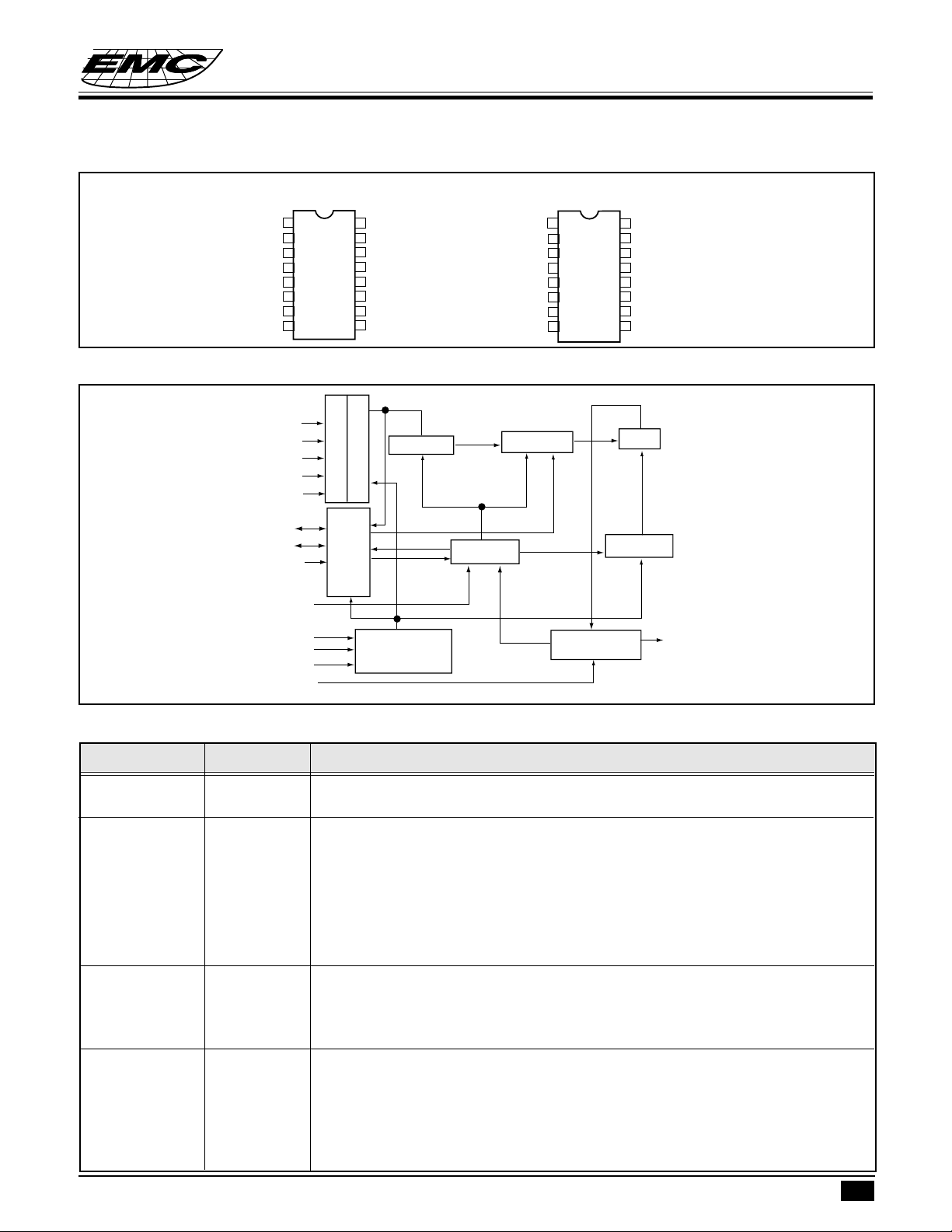
PIN ASSIGNMENTS
EM83702
ALL IN ONE MOUSE CONTROLLER
EM83702A
RS
1
MS
OSC.IN
OSC.OUT
RTS
RXD
VSS
R
16
2
15
3
14
4
13
5
12
6
11
7
10
8
9
FUNCTIONAL BLOCK DIAGRAM
OPT
OSC.OUT
OSC.IN
RTS
X1
X2
Y1
Y2
L
M
R
MS
RS
D
M
E
N
M
M
T
O
O
U
E
I
T
N
C
S
I
T
E
O
T
O
N
Y
R
D
E
B
O
U
N
C
E
V
DD
OPT
Y2
Y1
X2
X1
L
M
I
I
SYSTEM CLOCK
GENERATOR
COUNTER
MODE
SELECTOR
RS
OPT
MS
OSC.IN
OSC.OUT
RTS
RXD
VSS
MULTIPLEXER
EM83702B
1
16
2
15
3
14
4
13
5
12
6
11
7
10
8
9
CONTROLLER
LEVEL-SHIFT
CIRCUIT
V
DD
Y2
Y1
X2
X1
L
M
R
P/S
TIMING
RXD
PIN DESCRIPTIONS
Symbol I/O Function
RS I Crystal type select : "0" or floating, select 32.768KHz crystal. "1" select 3.58MHz
resonator.
MS I When this pin is connected to V
under the microsoft mode only. If the pin is connected to V
will operate under the mouse system mode.
However if this pin is "floating", then EM83702 is on the “power on initiation”
situation and if any one of three buttons is chosen, thence EM83702 will operate
under the mouse mode. And while the whole system is on “power on initiation”.No
key is chosen then operation will be under microsoft mode.
OSC.IN I A built-in inverter provides oscillation with 32.768 KHz crystal or 3.58MHz
OSC.OUT resonator.
Several counters used to decrease the frequency of oscillation and create 1200 baud
rate, key-switches debounce and photo-couple sensor scanning clock,etc.
RTS I Positive power input.
The signal is sent by mouse driver from computer to the mouse to select
a mode. During the reset time, EM83702 echoes the selected mode to the RXD line
after the reset pulse signal of the RTS line. RXD will send out CD(H) code if
it is under the microsoft mode. RXD will send out two byte C8(H) code if it is under
the mouse system mode in EM83702.
, then EM83702 is assigned to operate
DD
, then EM83702
SS
* This specification are subject to be changed without notice.
4.15.1996
2
Page 3
EM83702
ALL IN ONE MOUSE CONTROLLER
Symbol I/O Function
RXD O There are 8 or 7 bits in each data byte.
Using parallel-in and serial-out components, the data bytes are shifted out from bit
0 through the high bits. EM83702 will transmit the data while the status of three
keyswitches or the state of the horizontal counter or vertical counter is changed.
V
SS
Negative power input.
R I Three key-switches exert seven different combinations totally.
M I/O Both key-pressed and key-released signals will be sent accomplanied with
L I/O horizontal and vertical state. The status of the key-switches will be preserved,
whenever the value of horizontal or vertical counters will present at RXD. And the
debounce interval for both key-press and key-release is 13 ms.
In testing mode, L and M are the outputs of motion detecdor. Using R key can select
the two outputs X1, X2 or Y1,Y2. This feature can help manufacturer to adjust the
phase of four photo-couples for improving the yield.
X1 I Four photo-couple signals denote UP, DOWN, LEFT and RIGHT state. If
X2 EM83702 is in 1200 baud rate on non-auto speed mode, the system provides 40
Y1 transmission cycles per second in microsoft mode to the utmost. In mouse system
Y2 mode, the cycles are 24 maxiun. During the scaning period, as long as the photo-
couples change their states, the value of vertical or horizontal counter will increase
or decrease accordingly.
OPT I Whenever OPT is connected to V
V
DD
Power.
, the chip will enter testing mode.
DD
FUNCTION DESCRIPTIONS
A) Operating Mode
Mouse system mode
Anytime the mouse changes its state, including the key-switches and the photo-couple sensors, EM83702 will
detect the result and transmit to RS-232C. Mouse system transmits the result with five bytes in 1200 baud
rate. Each byte contains 10 bits, one start bit, one stop bit and eight data bits. The first byte represents
the key-switches status. The second byte denote the number counted by the horizontal counter. The third byte
conveys the number accumulated by the vertical counter. If the mouse is moved faster, the photo-couple
sensors detect the “change state” and output the record, excessive horizontal counter will be transported
through the fourth byte, and vertical counter through the fifth byte. Otherwise, the fourth and fifth byte are zero.
Output bytes arrange:
bit no ...... 7 6 5 4 3 2 1 0
1st byte...... 1 0 0 0 0 L’ M’ R’*
2nd byte...... H7 H6 H5 H4 H3 H2 H1 H0
3rd byte...... V7 V6 V5 V4 V3 V2 V1 V0
4th byte...... H7 H6 H5 H4 H3 H2 H1 H0
5th byte...... V7 V6 V5 V4 V3 V2 V1 V0
* ‘ denotes complement
* This specification are subject to be changed without notice.
4.15.1996
3
Page 4

EM83702
ALL IN ONE MOUSE CONTROLLER
(B) Microsoft mode
In microsoft mode, the transmission cycle consists of three bytes. Each byte is divided into one start bit, seven
data bits and two stop bit. The first byte contains “L”,”R” switch status and four bits of the two most significant bits in horizontal counter and vertical counter. The next byte represents the value accumulated by
horizontal counter, the last byte is the data of the vertical counter. Notice that “M” key-switch is not active
in the microsoft mode and the vertical data is transmited in 2’s complement.
Output byte arrange:
bit no ...... 6 5 4 3 2 1 0
1st byte...... 1 L R V7' V6' H7 H6
2nd byte...... 0 H5 H4 H3 H2 H1 H0
3rd byte...... 0 V5' V4' V3' V2' V1' V0'
(C) Testing mode
Whenever OPT is connected to VDD, the chip will enter buyer’s testing mode. The X direction output signals
of comparators will present to L and M pin. Pressing “R” key can toggle the output from X direction to Y
direction.
(D) Echo mode
RXD will send out CD(H) code when RTS rise from low to high under microsoft mode. Under mouse
system mode, when RTS rise from low to high, the RXD pin EM83702 will send out two byte C8(H) code.
* This specification are subject to be changed without notice.
4.15.1996
4
Page 5

ALL IN ONE MOUSE CONTROLLER
ABSOLUTE MAXIMUM RATINGS
Parameter Min. Max. Unit
EM83702
Supply voltage VDD-V
RTS-V
SS
SS
-0.3 7.0 V
-0.3 14 V
Temperature under bias 0 70 °C
Storage temperature range -65 150 °C
Power dissipation - 500 mW
DC ELECTRICAL CHARACTERISTICS ( T
= 25°C to 70 °C )
A
Parameter Sym. Min. Typ. Max. Unit.
Operating voltage V
V
Operating current (V
Operating current (V
Operating current (V
Operating current (V
RTS operating current (V
RTS operating current (V
=5.4V,RTS=VDD, 32.768KHz, no load) Iop - - 0.6 mA
DD
=6.2V,RTS=VDD, 32.768KHz, no load) Iop 3 - - mA
DD
=5.4V,RTS=VDD, 3.58KHz, no load) Iop - - 1.6 mA
DD
=6.2V,RTS=VDD, 3.58KHz, no load) Iop 4 - - mA
DD
=5.6V,RTS=11V) I
DD
=5.6V,RTS=11.8V) I
DD
DD
RTS
RTS
RTS
- - 6.5 V
- - 13 V
- - 0.6 mA
3- - mA
RXD high output voltage Irh 2.0 - - mA
(Vrh=Vrts-2.6V)
RXD low output voltage Irl - - -2.0 mA
(Vrl=Vss+2.6V)
X1,X2,Y1,Y2 low input voltage Vpl - - 0.7 V
X1,X2,Y1,Y2 high input voltage Vph 1.3 - - V
X1,X2,Y1,Y2 input current Ipi 57 - 104 µA
( pull low resistor Vds=1.0V )
RTS high input voltage Vt+ 9.6 - - V
RTS low input voltage Vt- - - 6.8 V
Low input voltage , other pins Vail - - 1.5 V
High input voltage , other pins Vaih 3.5 - - V
L,M,R,OPT input current Imi 18.6 - 56 µA
(pull low resistor Vds=5.6V)
RS,OSC.IN,L,M,R,X1, X2,Y1,Y2,OPT Iil 0 - 1.0 µA
input leakage current
( Vin = 0V )
RS,OSC.IN input leakage current Iih -1.0 - 0 µA
( Vin = 5.6V)
* All voltages in above table are compared with VSS.
* All parameters in above table are tested under V
DD
* This specification are subject to be changed without notice.
=5.6V.
4.15.1996
5
Page 6

X1,X2,Y1,Y2 INPUT IMPEDANCE
R
17.0 K
MAX.
16.0 K
15.0 K
14.0 K
TYP.
13.0 K
12.0 K
MIN.
11.0 K
10.0 K
9.0 K
8.0 K
7.0 K
6.0 K
5.0 K
4.0 K
3.0 K
2.0 K
1.0 K
0
10.0M
1.0 2.0 3.0
VOLTS (LIN)
AC ELECTRICAL CHARACTERISTICS (TA=0°C to 70°C)
EM83702
ALL IN ONE MOUSE CONTROLLER
4.0
5.0
Parameters Sym. Min. Typ. Max. Unit
Key debounce Tkd - 13 - ms
Transmission time mouse (1200) Tms - 41.1 - ms
Transmission time microsoft (1200) Tmx - 24.7 - ms
Start bit time (1200) Ts - 0.85 - ms
Data bit time (1200) Td - 0.82 - ms
Stop bit time (1200) Tp - 0.82 - ms
Mode code delay time (1200) Trd 11.9 - 14 ms
Rising edge crossed width Tr 15 - - us
Falling edge crossed width Tf 15 - - us
AC TIMING TEST POINT :
Output:
RXD pin
Input:
X1, X2, Y1, Y2, pin
VRTS-2.4V
VSS+0.8V
1.3V
0.7V
RTS pin
Other pin
* This specification are subject to be changed without notice.
2V
VSS
V
DD
VSS
DD
4.15.1996
6
Page 7

TIMING DIAGRAM
(A) P/S output:
Key in/release
Mouse RXD
Microsoft RXD
(B) Bytes structure:
Mouse RXD
Tms
Tmx
1st 2nd
3rd
EM83702
ALL IN ONE MOUSE CONTROLLER
Tms
Tmx
4th 5th
Microsoft RXD
(C) Bits structure:
(1) Mouse
RXD LINE
Data bit no.
(2) Microsoft
RXD LINE
Data bit no.
#(D) mode select timing:
(1) Mouse system
RTS
RXD
Reset code
"C8" Bit no.
1st 2nd
0Td1
Ts
0Td1
Ts
Trd
>
<Trb
>
two byte "C8" code
Ts 0 1
3rd
Td
Td
2
4Td5Td6
4Td5Td6
4
3
2Td3
Td
2Td3
Td
<
7
Td
Td
Td
5
Tp
6
Tp
Tp
7Tp
01
01
(2) Microsoft
RTS
Trd
>
<
RXD
Reset code
>
"CD" code
<
Ts 0 1
2
"CD" Bit no.
* This specification are subject to be changed without notice.
5
4
3
6
7Tp
4.15.1996
7
Page 8

#(E) Photo-couples pulse width
X1 (Y1)
X1(Y1)
Tr Tf
EM83702 I/O pin equivalent circuit:
RS, R, M, L, OPT: OSC.IN, OSC.OUT:
AUT (R,M,L,OPT)
RS (R,M,L,OPT)
INTERNAL SIGNAL
EM83702
ALL IN ONE MOUSE CONTROLLER
INTERNAL SYSTEM CLOCK
OSC.IN
L, M, R, MS: RTS, RXD:
RTS
VDD
RTS
VDD
L
M
R
POWER ON RESET
X1(Y1) PHASE DIGITAL SIGNAL
X2(Y2) PHASE DIGITAL SIGNAL
VCC
MS
TEST MODE ENABLE
Q
D
CLK
MODE SELECTION
RXD CONTROL SIGNAL
RXD CONTROL SIGNAL
X1, X2, Y1, Y2:
OSC.OUT
R
R
R
R
RXD
RXD
RTS INTERNAL SIGNAL
RTS INTERNAL SIGNAL
4.5R
VCC
+
PHASE DIGITAL SIGNAL
X1(X2,Y1,Y2)
-
R
* This specification are subject to be changed without notice.
4.15.1996
8
Page 9

APPLICATION CIRCUIT
Mechanical Mouse
EM83702
ALL IN ONE MOUSE CONTROLLER
GND
16
DD
V
15
OPT
14
Y2
Y
13
Y1
12
X2
X
11
X1
10
10µF
9
L
M
EM83702A
MS
OSC.IN
3
OSC.OUT
5
4
RTS
6
RS
1
2
RXD
SS
R
V
7
8
(3.58MHz)
32768 Hz
* This specification are subject to be changed without notice.
RTS
RXD
TXD
4.15.1996
9
Page 10

Optomechanical Mouse
EM83702
ALL IN ONE MOUSE CONTROLLER
SG
10µF
R
15
OPT
14
13
Y1
Y2
16
DD
V
11
12
X1
X2
9
10
L
M
EM83702A
6
RXD
RXD
7
SS
V
TXD
R
8
RS
1
OSC.IN
MS
3
2
OSC.OUT
4
32768 Hz
(3.58MHz)
RTS
5
RTS
* This specification are subject to be changed without notice.
4.15.1996
10
Page 11

Optomechanical Mouse
EM83702
ALL IN ONE MOUSE CONTROLLER
SG
10µF
R
16
DD
V
2
OPT
15
Y2
14
Y1
13
X2
12
X1
11
10
L
M
EM83702B
MS
4
OSC.IN
5
32768 Hz
RS
3
1
RTS
OSC.OUT
6
(3.58MHz)
RTS
7
RXD
RXD
8
SS
V
TXD
R
9
* This specification are subject to be changed without notice.
4.15.1996
11
 Loading...