


 Loading...
ELPID HM5225405BLTT-75, HM5225405BLTT-A6, HM5225405BLTT-B6, HM5225405BTT-75, HM5225405BTT-A6 Datasheet
...HM5225165B-75/A6/B6
HM5225805B-75/A6/B6
HM5225405B-75/A6/B6
256M LVTTL interface SDRAM
133 MHz/100 MHz
4-Mword × 16-bit × 4-bank/8-Mword × 8-bit × 4-bank /16-Mword × 4-bit × 4-bank
PC/133, PC/100 SDRAM
E0082H10 (1st edition) (Previous ADE-203-1073B (Z))
Jan. 31, 2001
Description
The HM5225165B is a 256-Mbit SDRAM organized as 4194304-word × 16-bit × 4 bank. The HM5225805B is a 256-Mbit SDRAM organized as 8388608-word × 8-bit × 4 bank. The HM5225405B is a 256-Mbit SDRAM organized as 16777216-word × 4-bit × 4 bank. All inputs and outputs are referred to the rising edge of the clock input. It is packaged in standard 54-pin plastic TSOP II.
Features
•3.3 V power supply
•Clock frequency: 133 MHz/100 MHz (max)
•LVTTL interface
•Single pulsed RAS
•4 banks can operate simultaneously and independently
•Burst read/write operation and burst read/single write operation capability
•Programmable burst length: 1/2/4/8
•2 variations of burst sequence
Sequential (BL = 1/2/4/8)
Interleave (BL = 1/2/4/8)
•Programmable CAS latency: 2/3
Elpida Memory, Inc. is a joint venture DRAM company of NEC Corporation and Hitachi, Ltd.

HM5225165B/HM5225805B/HM5225405B-75/A6/B6
•Byte control by DQM : DQM (HM5225805B/HM5225405B)
:DQMU/DQML (HM5225165B)
•Refresh cycles: 8192 refresh cycles/64 ms
•2 variations of refresh
Auto refresh
Self refresh
Ordering Information
Type No. |
Frequency |
CAS latency |
Package |
HM5225165BTT-75*1 |
133 MHz |
3 |
400-mil 54-pin plastic TSOP II (TTP-54D) |
HM5225165BTT-A6 |
100 MHz |
2/3 |
|
HM5225165BTT-B6*2 |
100 MHz |
3 |
|
|
|
|
|
HM5225165BLTT-75*1 |
133 MHz |
3 |
|
HM5225165BLTT-A6 |
100 MHz |
2/3 |
|
HM5225165BLTT-B6*2 |
100 MHz |
3 |
|
|
|
|
|
HM5225805BTT-75*1 |
133 MHz |
3 |
|
HM5225805BTT-A6 |
100 MHz |
2/3 |
|
HM5225805BTT-B6*2 |
100 MHz |
3 |
|
|
|
|
|
HM5225805BLTT-75*1 |
133 MHz |
3 |
|
HM5225805BLTT-A6 |
100 MHz |
2/3 |
|
HM5225805BLTT-B6*2 |
100 MHz |
3 |
|
|
|
|
|
HM5225405BTT-75*1 |
133 MHz |
3 |
|
HM5225405BTT-A6 |
100 MHz |
2/3 |
|
HM5225405BTT-B6*2 |
100 MHz |
3 |
|
|
|
|
|
HM5225405BLTT-75*1 |
133 MHz |
3 |
|
HM5225405BLTT-A6 |
100 MHz |
2/3 |
|
HM5225405BLTT-B6*2 |
100 MHz |
3 |
|
Notes: 1. 100 MHz operation at CAS latency = 2. 2. 66 MHz operation at CAS latency = 2.
Data Sheet E0082H10
2

HM5225165B/HM5225805B/HM5225405B-75/A6/B6
Pin Arrangement (HM5225165B)
|
|
|
|
|
54-pin TSOP |
|
|
|
VCC |
|
|
|
1 |
54 |
|
VSS |
|
|
|
|
2 |
|
||||
DQ0 |
|
|
|
53 |
|
DQ15 |
||
VCCQ |
|
|
3 |
52 |
|
VSSQ |
||
|
|
|
||||||
|
|
|
4 |
|
||||
DQ1 |
|
|
|
51 |
|
DQ14 |
||
DQ2 |
|
|
5 |
50 |
|
DQ13 |
||
|
|
|
||||||
VSSQ |
|
|
|
6 |
49 |
|
VCCQ |
|
|
|
|
||||||
|
|
|
7 |
|
||||
DQ3 |
|
|
|
48 |
|
DQ12 |
||
DQ4 |
|
|
|
8 |
47 |
|
DQ11 |
|
|
|
|
||||||
VCCQ |
|
|
9 |
46 |
|
VSSQ |
||
|
|
|
||||||
|
|
|
10 |
|
||||
DQ5 |
|
|
|
45 |
|
DQ10 |
||
DQ6 |
|
|
11 |
44 |
|
DQ9 |
||
|
|
|
||||||
VSSQ |
|
|
|
12 |
43 |
|
VCCQ |
|
|
|
|||||||
|
|
|
13 |
|
||||
DQ7 |
|
|
|
42 |
|
DQ8 |
||
VCC |
|
|
14 |
41 |
|
VSS |
||
|
|
|
||||||
|
|
|
15 |
|
||||
DQML |
|
|
|
40 |
|
NC |
||
WE |
|
|
16 |
39 |
|
DQMU |
||
|
|
|
|
|||||
CAS |
|
|
17 |
38 |
|
CLK |
||
|
|
|
|
|||||
RAS |
|
|
18 |
37 |
|
CKE |
||
|
|
|
|
|||||
CS |
|
|
19 |
36 |
|
A12 |
||
|
|
|
|
|||||
BA0 |
|
|
20 |
35 |
|
A11 |
||
|
|
|
|
|||||
BA1 |
|
|
21 |
34 |
|
A9 |
||
|
|
|
|
|||||
A10 |
|
|
22 |
33 |
|
A8 |
||
|
|
|
|
|||||
A0 |
|
|
23 |
32 |
|
A7 |
||
|
|
|
|
|||||
A1 |
|
|
24 |
31 |
|
A6 |
||
|
|
|
|
|||||
A2 |
|
|
|
25 |
30 |
|
A5 |
|
|
|
|
|
|||||
A3 |
|
|
|
26 |
29 |
|
A4 |
|
|
|
|
|
|||||
VCC |
|
|
|
|
27 |
28 |
|
VSS |
|
|
|
|
|
||||
|
|
|
|
|
|
|||
(Top view)
Pin Description
Pin name |
Function |
|
Pin name |
Function |
A0 to A12, |
Address input |
|
WE |
Write enable |
BA0, BA1 |
|
|
|
|
|
|
|
|
|
|
Row address |
A0 to A12 |
DQMU/DQML |
Input/output mask |
|
|
|
|
|
|
Column address |
A0 to A8 |
CLK |
Clock input |
|
|
|
|
|
|
Bank select address |
BA0/BA1 (BS) |
CKE |
Clock enable |
|
|
|
|
|
DQ0 to DQ15 |
Data-input/output |
|
VCC |
Power for internal circuit |
CS |
Chip select |
|
VSS |
Ground for internal circuit |
RAS |
Row address strobe command |
VCCQ |
Power for DQ circuit |
|
|
|
|
|
|
CAS |
Column address strobe command |
VSSQ |
Ground for DQ circuit |
|
|
|
|
|
|
|
|
|
NC |
No connection |
|
|
|
|
|
Data Sheet E0082H10
3
HM5225165B/HM5225805B/HM5225405B-75/A6/B6
Pin Arrangement (HM5225805B)
|
|
|
|
|
54-pin TSOP |
|
|
|
|
|
|
|
|
|
|
|
|
VCC |
|
|
|
1 |
54 |
|
VSS |
|
|
|
|
2 |
|
||||
DQ0 |
|
|
|
53 |
|
DQ7 |
||
VCCQ |
|
|
3 |
52 |
|
VSSQ |
||
|
|
|
||||||
|
|
|
4 |
|
||||
NC |
|
|
|
51 |
|
NC |
||
DQ1 |
|
|
5 |
50 |
|
DQ6 |
||
|
|
|
||||||
VSSQ |
|
|
|
6 |
49 |
|
VCCQ |
|
|
|
|
||||||
|
|
|
7 |
|
||||
NC |
|
|
|
48 |
|
NC |
||
DQ2 |
|
|
|
8 |
47 |
|
DQ5 |
|
|
|
|
||||||
VCCQ |
|
|
9 |
46 |
|
VSSQ |
||
|
|
|
||||||
|
|
|
10 |
|
||||
NC |
|
|
|
45 |
|
NC |
||
DQ3 |
|
|
11 |
44 |
|
DQ4 |
||
|
|
|
||||||
VSSQ |
|
|
|
12 |
43 |
|
VCCQ |
|
|
|
|||||||
|
|
|
13 |
|
||||
NC |
|
|
|
42 |
|
NC |
||
VCC |
|
|
14 |
41 |
|
VSS |
||
|
|
|
||||||
|
|
|
15 |
|
||||
NC |
|
|
|
40 |
|
NC |
||
WE |
|
|
16 |
39 |
|
DQM |
||
|
|
|
|
|||||
CAS |
|
|
17 |
38 |
|
CLK |
||
|
|
|
|
|||||
RAS |
|
|
18 |
37 |
|
CKE |
||
|
|
|
|
|||||
CS |
|
|
19 |
36 |
|
A12 |
||
|
|
|
|
|||||
BA0 |
|
|
20 |
35 |
|
A11 |
||
|
|
|
|
|||||
BA1 |
|
|
21 |
34 |
|
A9 |
||
|
|
|
|
|||||
A10 |
|
|
22 |
33 |
|
A8 |
||
|
|
|
|
|||||
A0 |
|
|
23 |
32 |
|
A7 |
||
|
|
|
|
|||||
A1 |
|
|
24 |
31 |
|
A6 |
||
|
|
|
|
|||||
A2 |
|
|
|
25 |
30 |
|
A5 |
|
|
|
|
|
|||||
A3 |
|
|
|
26 |
29 |
|
A4 |
|
|
|
|
|
|||||
VCC |
|
|
|
|
27 |
28 |
|
VSS |
|
|
|
|
|
||||
|
|
|
|
|
|
|||
(Top view)
Pin Description
Pin name |
Function |
|
Pin name |
Function |
A0 to A12, |
Address input |
|
WE |
Write enable |
BA0, BA1 |
|
|
|
|
|
|
|
|
|
|
Row address |
A0 to A12 |
DQM |
Input/output mask |
|
|
|
|
|
|
Column address |
A0 to A9 |
CLK |
Clock input |
|
|
|
|
|
|
Bank select address |
BA0/BA1 (BS) |
CKE |
Clock enable |
|
|
|
|
|
DQ0 to DQ7 |
Data-input/output |
|
VCC |
Power for internal circuit |
CS |
Chip select |
|
VSS |
Ground for internal circuit |
RAS |
Row address strobe command |
VCCQ |
Power for DQ circuit |
|
|
|
|
|
|
CAS |
Column address strobe command |
VSSQ |
Ground for DQ circuit |
|
|
|
|
|
|
|
|
|
NC |
No connection |
|
|
|
|
|
Data Sheet E0082H10
4

HM5225165B/HM5225805B/HM5225405B-75/A6/B6
Pin Arrangement (HM5225405B)
|
|
|
|
|
54-pin TSOP |
|
|
|
|
|
|
|
|
|
|
|
|
VCC |
|
|
|
1 |
54 |
|
VSS |
|
|
|
|
2 |
|
||||
NC |
|
|
|
53 |
|
NC |
||
VCCQ |
|
|
3 |
52 |
|
VSSQ |
||
|
|
|
||||||
|
|
|
4 |
|
||||
NC |
|
|
|
51 |
|
NC |
||
DQ0 |
|
|
5 |
50 |
|
DQ3 |
||
|
|
|
||||||
VSSQ |
|
|
|
6 |
49 |
|
VCCQ |
|
|
|
|
||||||
|
|
|
7 |
|
||||
NC |
|
|
|
48 |
|
NC |
||
NC |
|
|
|
8 |
47 |
|
NC |
|
|
|
|
||||||
VCCQ |
|
|
9 |
46 |
|
VSSQ |
||
|
|
|
||||||
|
|
|
10 |
|
||||
NC |
|
|
|
45 |
|
NC |
||
DQ1 |
|
|
11 |
44 |
|
DQ2 |
||
|
|
|
||||||
VSSQ |
|
|
|
12 |
43 |
|
VCCQ |
|
|
|
|||||||
|
|
|
13 |
|
||||
NC |
|
|
|
42 |
|
NC |
||
VCC |
|
|
14 |
41 |
|
VSS |
||
|
|
|
||||||
|
|
|
15 |
|
||||
NC |
|
|
|
40 |
|
NC |
||
WE |
|
|
16 |
39 |
|
DQM |
||
|
|
|
|
|||||
CAS |
|
|
17 |
38 |
|
CLK |
||
|
|
|
|
|||||
RAS |
|
|
18 |
37 |
|
CKE |
||
|
|
|
|
|||||
CS |
|
|
19 |
36 |
|
A12 |
||
|
|
|
|
|||||
BA0 |
|
|
20 |
35 |
|
A11 |
||
|
|
|
|
|||||
BA1 |
|
|
21 |
34 |
|
A9 |
||
|
|
|
|
|||||
A10 |
|
|
22 |
33 |
|
A8 |
||
|
|
|
|
|||||
A0 |
|
|
23 |
32 |
|
A7 |
||
|
|
|
|
|||||
A1 |
|
|
24 |
31 |
|
A6 |
||
|
|
|
|
|||||
A2 |
|
|
|
25 |
30 |
|
A5 |
|
|
|
|
|
|||||
A3 |
|
|
|
26 |
29 |
|
A4 |
|
|
|
|
|
|||||
VCC |
|
|
|
|
27 |
28 |
|
VSS |
|
|
|
|
|
||||
|
|
|
|
|
|
|||
(Top view)
Pin Description
Pin name |
Function |
|
Pin name |
Function |
A0 to A12, |
Address input |
|
WE |
Write enable |
BA0, BA1 |
|
|
|
|
|
|
|
|
|
|
Row address |
A0 to A12 |
DQM |
Input/output mask |
|
|
|
|
|
|
Column address |
A0 to A9, A11 |
CLK |
Clock input |
|
|
|
|
|
|
Bank select address |
BA0/BA1 (BS) |
CKE |
Clock enable |
|
|
|
|
|
DQ0 to DQ3 |
Data-input/output |
|
VCC |
Power for internal circuit |
CS |
Chip select |
|
VSS |
Ground for internal circuit |
RAS |
Row address strobe command |
VCCQ |
Power for DQ circuit |
|
|
|
|
|
|
CAS |
Column address strobe command |
VSSQ |
Ground for DQ circuit |
|
|
|
|
|
|
|
|
|
NC |
No connection |
|
|
|
|
|
Data Sheet E0082H10
5
HM5225165B/HM5225805B/HM5225405B-75/A6/B6
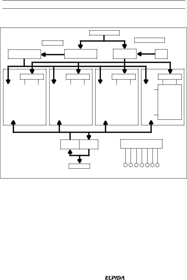
Block Diagram (HM5225165B)
A0 to A12, BA0, BA1
A0 to A12, BA0, BA1
A0 to A8
Column address |
Column address |
Row address |
counter |
buffer |
buffer |
Row decoder |
Row decoder |
Row decoder |
Columndecoder |
bus |
|
Memory array |
|
Columndecoder |
bus |
|
Memory array |
|
Columndecoder |
bus |
|
Memory array |
|
Columndecoder |
bus |
|
|
|
|
|
|
|||||||||||
amplifierSense & I/O |
|
X 16 bit |
|
amplifierSense & I/O |
|
X 16 bit |
|
amplifierSense & I/O |
|
X 16 bit |
|
amplifierSense & I/O |
||||
|
|
|
Bank 0 |
|
|
|
|
Bank 1 |
|
|
|
|
Bank 2 |
|
|
|
|
|
|
8192 row |
|
|
|
|
8192 row |
|
|
|
|
8192 row |
|
|
|
|
|
|
X 512 column |
|
|
|
|
X 512 column |
|
|
|
|
X 512 column |
|
|
|
|
|
|
|
|
|
|
|
|
|
|
|
|
|
|
|
|
|
|
|
|
|
|
|
|
|
|
|
|
|
|
|
|
|
Refresh
counter
Row decoder
Memory array
Bank 3
8192 row
X 512 column X 16 bit
Input |
Output |
Control logic & |
buffer |
buffer |
timing generator |
DQ0 to DQ15 |
|
|
CLK |
CKE |
CS |
RAS |
CAS |
WE |
DQMU /DQML |
Data Sheet E0082H10
6

HM5225165B/HM5225805B/HM5225405B-75/A6/B6
Block Diagram (HM5225805B)
|
|
|
A0 to A12, BA0, BA1 |
|
|
||
|
|
|
|
|
|
|
|
|
|
|
|
|
|
|
|
|
|
|
|
|
|
|
A0 to A12, BA0, BA1 |
A0 to A9 |
|
|
|
|
|
||
|
|
|
|
|
|
|
|
|
|
|
|
|
|
|
|
Column address |
Column address |
Row address |
counter |
buffer |
buffer |
Row decoder |
Row decoder |
Row decoder |
Columndecoder |
bus |
|
Memory array |
|
Columndecoder |
bus |
|
Memory array |
|
Columndecoder |
bus |
|
Memory array |
|
Columndecoder |
bus |
|
|
|
|
|
|
|||||||||||
amplifierSense & I/O |
|
X 8 bit |
|
amplifierSense & I/O |
|
X 8 bit |
|
amplifierSense & I/O |
|
X 8 bit |
|
amplifierSense & I/O |
||||
|
|
|
Bank 0 |
|
|
|
|
Bank 1 |
|
|
|
|
Bank 2 |
|
|
|
|
|
|
8192 row |
|
|
|
|
8192 row |
|
|
|
|
8192 row |
|
|
|
|
|
|
X 1024 column |
|
|
|
|
X 1024 column |
|
|
|
|
X 1024 column |
|
|
|
|
|
|
|
|
|
|
|
|
|
|
|
|
|
|
|
|
|
|
|
|
|
|
|
|
|
|
|
|
|
|
|
|
|
Refresh
counter
Row decoder
Memory array
Bank 3
8192 row
X 1024 column X 8 bit
Input |
Output |
Control logic & |
buffer |
buffer |
timing generator |
DQ0 to DQ7 |
CLK |
CKE |
CS |
RAS |
CAS |
WE |
DQM |
Data Sheet E0082H10
7

HM5225165B/HM5225805B/HM5225405B-75/A6/B6
Block Diagram (HM5225405B)
A0 to A12, BA0, BA1
A0 to A12, BA0, BA1
A0 to A9, A11
Column address |
Column address |
Row address |
counter |
buffer |
buffer |
Row decoder |
Row decoder |
Row decoder |
Columndecoder |
bus |
|
Memory array |
|
Columndecoder |
bus |
|
Memory array |
|
Columndecoder |
bus |
|
Memory array |
|
Columndecoder |
bus |
|
|
|
|
|
|
|||||||||||
amplifierSense & I/O |
|
X 4 bit |
|
amplifierSense & I/O |
|
X 4 bit |
|
amplifierSense & I/O |
|
X 4 bit |
|
amplifierSense & I/O |
||||
|
|
|
Bank 0 |
|
|
|
|
Bank 1 |
|
|
|
|
Bank 2 |
|
|
|
|
|
|
8192 row |
|
|
|
|
8192 row |
|
|
|
|
8192 row |
|
|
|
|
|
|
X 2048 column |
|
|
|
|
X 2048 column |
|
|
|
|
X 2048 column |
|
|
|
|
|
|
|
|
|
|
|
|
|
|
|
|
|
|
|
|
|
|
|
|
|
|
|
|
|
|
|
|
|
|
|
|
|
Refresh
counter
Row decoder
Memory array
Bank 3
8192 row
X 2048 column X 4 bit
Input |
Output |
Control logic & |
buffer |
buffer |
timing generator |
DQ0 to DQ3 |
|
|
CLK |
CKE |
CS |
RAS |
CAS |
WE |
DQM |
Data Sheet E0082H10
8

HM5225165B/HM5225805B/HM5225405B-75/A6/B6
Pin Functions
CLK (input pin): CLK is the master clock input to this pin. The other input signals are referred at CLK rising edge.
CS (input pin): When CS is Low, the command input cycle becomes valid. When CS is High, all inputs are ignored. However, internal operations (bank active, burst operations, etc.) are held.
RAS, CAS, and WE (input pins): Although these pin names are the same as those of conventional DRAMs, they function in a different way. These pins define operation commands (read, write, etc.) depending on the combination of their voltage levels. For details, refer to the command operation section.
A0 to A12 (input pins): Row address (AX0 to AX12) is determined by A0 to A12 level at the bank active command cycle CLK rising edge. Column address (AY0 to AY8; HM5225165B, AY0 to AY9; HM5225805B, AY0 to AY9, AY11; HM5225405B) is determined by A0 to A8, A9 or A11 (A8; HM5225165B, A9; HM5225805B, A9, A11; HM5225405B) level at the read or write command cycle CLK rising edge. And this column address becomes burst access start address. A10 defines the precharge mode. When A10 = High at the precharge command cycle, all banks are precharged. But when A10 = Low at the precharge command cycle, only the bank that is selected by BA0/BA1 (BS) is precharged. For details refer to the command operation section.
BA0/BA1 (input pin): BA0/BA1 are bank select signal (BS). The memory array of the HM5225165B, HM5225805B, the HM5225405B is divided into bank 0, bank 1, bank 2 and bank 3. HM5225165B contain 8192-row × 512-column × 16-bit. HM5225805B contain 8192-row × 1024-column× 8-bit. HM5225405B contain 8192-row × 2048-column × 4-bit. If BA0 is Low and BA1 is Low, bank 0 is selected. If BA0 is Low and BA1 is High, bank 1 is selected. If BA0 is High and BA1 is Low, bank 2 is selected. If BA0 is High and BA1 is High, bank 3 is selected.
CKE (input pin): This pin determines whether or not the next CLK is valid. If CKE is High, the next CLK rising edge is valid. If CKE is Low, the next CLK rising edge is invalid. This pin is used for power-down mode, clock suspend mode and self refresh mode.
DQM, DQMU/DQML (input pins): DQM, DQMU/DQML controls input/output buffers.
Read operation: If DQM, DQMU/DQML is High, the output buffer becomes High-Z. If the DQM, DQMU/DQML is Low, the output buffer becomes Low-Z. (The latency of DQM, DQMU/DQML during reading is 2 clocks.)
Write operation: If DQM, DQMU/DQML is High, the previous data is held (the new data is not written). If DQM, DQMU/DQML is Low, the data is written. (The latency of DQM, DQMU/DQML during writing is 0 clock.)
DQ0 to DQ15 (DQ pins): Data is input to and output from these pins (DQ0 to DQ15; HM5225165B, DQ0 to DQ7; HM5225805B, DQ0 to DQ3; HM5225405B).
VCC and VCCQ (power supply pins): 3.3 V is applied. (VCC is for the internal circuit and VCCQ is for the output buffer.)
Data Sheet E0082H10
9

HM5225165B/HM5225805B/HM5225405B-75/A6/B6
VSS and VSSQ (power supply pins): Ground is connected. (VSS is for the internal circuit and VSSQ is for the output buffer.)
Command Operation
Command Truth Table
The SDRAM recognizes the following commands specified by the CS, RAS, CAS, WE and address pins.
|
|
CKE |
|
|
|
|
|
|
|
|
|
|
|
|
CS |
RAS |
CAS WE |
|
|
A0 |
|
Command |
Symbol |
n - 1 |
n |
BA0/BA1 |
A10 |
to A12 |
||||
|
|
|
|
|
|
|
|
|
|
|
Ignore command |
DESL |
H |
× |
H |
× |
× |
× × |
× |
× |
|
|
|
|
|
|
|
|
|
|
|
|
No operation |
NOP |
H |
× |
L |
H |
H |
H |
× |
× |
× |
|
|
|
|
|
|
|
|
|
|
|
Column address and read command |
READ |
H |
× |
L |
H |
L |
H |
V |
L |
V |
|
|
|
|
|
|
|
|
|
|
|
Read with auto-precharge |
READ A |
H |
× |
L |
H |
L |
H |
V |
H |
V |
|
|
|
|
|
|
|
|
|
|
|
Column address and write command |
WRIT |
H |
× |
L |
H |
L |
L |
V |
L |
V |
|
|
|
|
|
|
|
|
|
|
|
Write with auto-precharge |
WRIT A |
H |
× |
L |
H |
L |
L |
V |
H |
V |
|
|
|
|
|
|
|
|
|
|
|
Row address strobe and bank active |
ACTV |
H |
× |
L |
L |
H |
H |
V |
V |
V |
|
|
|
|
|
|
|
|
|
|
|
Precharge select bank |
PRE |
H |
× |
L |
L |
H |
L |
V |
L |
× |
|
|
|
|
|
|
|
|
|
|
|
Precharge all bank |
PALL |
H |
× |
L |
L |
H |
L |
× |
H |
× |
|
|
|
|
|
|
|
|
|
|
|
Refresh |
REF/SELF |
H |
V |
L |
L |
L |
H |
× |
× |
× |
|
|
|
|
|
|
|
|
|
|
|
Mode register set |
MRS |
H |
× |
L |
L |
L |
L |
V |
V |
V |
|
|
|
|
|
|
|
|
|
||
Note: H: VIH. L: VIL. × : VIH or VIL. V: |
Valid address input |
|
|
|
|
|
|
|
||
Ignore command [DESL]: When this command is set (CS is High), the SDRAM ignore command input at the clock. However, the internal status is held.
No operation [NOP]: This command is not an execution command. However, the internal operations continue.
Column address strobe and read command [READ]: This command starts a read operation. In addition, the start address of burst read is determined by the column address (AY0 to AY8; HM5225165B, AY0 to AY9; HM5225805B, AY0 to AY9, AY11; HM5225405B) and the bank select address (BS). After the read operation, the output buffer becomes High-Z.
Read with auto-precharge [READ A]: This command automatically performs a precharge operation after a burst read with a burst length of 1, 2, 4 or 8.
Data Sheet E0082H10
10
HM5225165B/HM5225805B/HM5225405B-75/A6/B6
Column address strobe and write command [WRIT]: This command starts a write operation. When the burst write mode is selected, the column address (AY0 to AY8; HM5225165B, AY0 to AY9; HM5225805B, AY0 to AY9, AY11; HM5225405B) and the bank select address (BA0/BA1) become the burst write start address. When the single write mode is selected, data is only written to the location specified by the column address (AY0 to AY8; HM5225165B, AY0 to AY9; HM5225805B, AY0 to AY9, AY11; HM5225405B) and the bank select address (BA0/BA1).
Write with auto-precharge [WRIT A]: This command automatically performs a precharge operation after a burst write with a length of 1, 2, 4 or 8, or after a single write operation.
Row address strobe and bank activate [ACTV]: This command activates the bank that is selected by BA0/BA1 (BS) and determines the row address (AX0 to AX12). When BA0 and BA1 are Low, bank 0 is activated. When BA0 is Low and BA1 is High, bank 1 is activated. When BA0 is High and BA1 is Low, bank 2 is activated. When BA0 and BA1 are High, bank 3 is activated.
Precharge selected bank [PRE]: This command starts precharge operation for the bank selected by BA0/BA1. If BA0 and BA1 are Low, bank 0 is selected. If BA0 is Low and BA1 is High, bank 1 is selected. If BA0 is High and BA1 is Low, bank 2 is selected. If BA0 and BA1 are High, bank 3 is selected.
Precharge all banks [PALL]: This command starts a precharge operation for all banks.
Refresh [REF/SELF]: This command starts the refresh operation. There are two types of refresh operation, the one is auto-refresh, and the other is self-refresh. For details, refer to the CKE truth table section.
Mode register set [MRS]: The SDRAM has a mode register that defines how it operates. The mode register is specified by the address pins (A0 to BA0 and BA1) at the mode register set cycle. For details, refer to the mode register configuration. After power on, the contents of the mode register are undefined, execute the mode register set command to set up the mode register.
Data Sheet E0082H10
11

HM5225165B/HM5225805B/HM5225405B-75/A6/B6
DQM Truth Table (HM5225165B)
|
|
CKE |
|
|
|
Command |
Symbol |
n - 1 |
n |
DQMU |
DQML |
|
|
|
|
|
|
Upper byte (DQ8 to DQ15) write enable/output enable |
ENBU |
H |
× |
L |
× |
|
|
|
|
|
|
Lower byte (DQ0 to DQ7) write enable/output enable |
ENBL |
H |
× |
× |
L |
|
|
|
|
|
|
Upper byte (DQ8 to DQ15) write inhibit/output disable |
MASKU |
H |
× |
H |
× |
|
|
|
|
|
|
Lower byte (DQ0 to DQ7) write inhibit/output disable |
MASKL |
H |
× |
× |
H |
|
|
|
|
|
|
Note: H: VIH. L: VIL. × : VIH or VIL. |
|
|
|
|
|
Write: IDID is needed. |
|
|
|
|
|
Read: IDOD is needed. |
|
|
|
|
|
DQM Truth Table (HM5225805B/HM5225405B)
|
|
CKE |
|
|
Command |
Symbol |
n - 1 |
n |
DQM |
|
|
|
|
|
Write enable/output enable |
ENB |
H |
× |
L |
|
|
|
|
|
Write inhibit/output disable |
MASK |
H |
× |
H |
|
|
|
|
|
Note: H: VIH. L: VIL. × : VIH or VIL. |
|
|
|
|
Write: IDID is needed. |
|
|
|
|
Read: IDOD is needed. |
|
|
|
|
The SDRAM can mask input/output data by means of DQM, DQMU/DQML.
DQMU masks the upper byte and DQML masks the lower byte. (HM5225165B)
During reading, the output buffer is set to Low-Z by setting DQM, DQMU/DQML to Low, enabling data output. On the other hand, when DQM, DQMU/DQML is set to High, the output buffer becomes High-Z, disabling data output.
During writing, data is written by setting DQM, DQMU/DQML to Low. When DQM, DQMU/DQML is set to High, the previous data is held (the new data is not written). Desired data can be masked during burst read or burst write by setting DQMU/DQML. For details, refer to the DQM, DQMU/DQML control section of the SDRAM operating instructions.
Data Sheet E0082H10
12

HM5225165B/HM5225805B/HM5225405B-75/A6/B6
CKE Truth Table
|
|
CKE |
|
|
|
|
|
|
Current state |
Command |
n - 1 |
n |
CS |
RAS |
CAS |
WE Address |
|
|
|
|
|
|
|
|
|
|
Active |
Clock suspend mode entry |
H |
L |
× |
× |
× |
× |
× |
|
|
|
|
|
|
|
|
|
Any |
Clock suspend |
L |
L |
× |
× |
× |
× |
× |
|
|
|
|
|
|
|
|
|
Clock suspend |
Clock suspend mode exit |
L |
H |
× |
× |
× |
× |
× |
|
|
|
|
|
|
|
|
|
Idle |
Auto-refresh command (REF) |
H |
H |
L |
L |
L |
H |
× |
|
|
|
|
|
|
|
|
|
Idle |
Self-refresh entry (SELF) |
H |
L |
L |
L |
L |
H |
× |
|
|
|
|
|
|
|
|
|
Idle |
Power down entry |
H |
L |
L |
H |
H |
H |
× |
|
|
|
|
|
|
|
|
|
|
|
H |
L |
H |
× |
× |
× |
× |
|
|
|
|
|
|
|
|
|
Self refresh |
Self refresh exit (SELFX) |
L |
H |
L |
H |
H |
H |
× |
|
|
|
|
|
|
|
|
|
|
|
L |
H |
H |
× |
× |
× |
× |
|
|
|
|
|
|
|
|
|
Power down |
Power down exit |
L |
H |
L |
H |
H |
H |
× |
|
|
|
|
|
|
|
|
|
|
|
L |
H |
H |
× |
× |
× |
× |
|
|
|
|
|
|
|
|
|
Note: H: VIH. L: VIL. × : VIH or VIL. |
|
|
|
|
|
|
|
|
Clock suspend mode entry: The SDRAM enters clock suspend mode from active mode by setting CKE to Low. If command is input in the clock suspend mode entry cycle, the command is valid. The clock suspend mode changes depending on the current status (1 clock before) as shown below.
ACTIVE clock suspend: This suspend mode ignores inputs after the next clock by internally maintaining the bank active status.
READ suspend and READ with Auto-precharge suspend: The data being output is held (and continues to be output).
WRITE suspend and WRIT with Auto-precharge suspend: In this mode, external signals are not accepted. However, the internal state is held.
Clock suspend: During clock suspend mode, keep the CKE to Low.
Clock suspend mode exit: The SDRAM exits from clock suspend mode by setting CKE to High during the clock suspend state.
IDLE: In this state, all banks are not selected, and completed precharge operation.
Auto-refresh command [REF]: When this command is input from the IDLE state, the SDRAM starts autorefresh operation. (The auto-refresh is the same as the CBR refresh of conventional DRAMs.) During the auto-refresh operation, refresh address and bank select address are generated inside the SDRAM. For every auto-refresh cycle, the internal address counter is updated. Accordingly, 8192 times are required to refresh the entire memory. Before executing the auto-refresh command, all the banks must be in the IDLE state. In addition, since the precharge for all banks is automatically performed after auto-refresh, no precharge command is required after auto-refresh.
Data Sheet E0082H10
13
HM5225165B/HM5225805B/HM5225405B-75/A6/B6
Self-refresh entry [SELF]: When this command is input during the IDLE state, the SDRAM starts selfrefresh operation. After the execution of this command, self-refresh continues while CKE is Low. Since selfrefresh is performed internally and automatically, external refresh operations are unnecessary.
Power down mode entry: When this command is executed during the IDLE state, the SDRAM enters power down mode. In power down mode, power consumption is suppressed by cutting off the initial input circuit.
Self-refresh exit: When this command is executed during self-refresh mode, the SDRAM can exit from selfrefresh mode. After exiting from self-refresh mode, the SDRAM enters the IDLE state.
Power down exit: When this command is executed at the power down mode, the SDRAM can exit from power down mode. After exiting from power down mode, the SDRAM enters the IDLE state.
Function Truth Table
The following table shows the operations that are performed when each command is issued in each mode of the SDRAM.
The following table assumes that CKE is high.
Current state |
CS |
RAS |
CAS |
WE |
Address |
Command |
Operation |
Precharge |
H |
× |
× |
× |
× |
DESL |
Enter IDLE after tRP |
|
|
|
|
|
|
|
|
|
L |
H |
H |
H |
× |
NOP |
Enter IDLE after tRP |
|
|
|
|
|
|
|
|
|
L |
H |
L |
H |
BA, CA, A10 |
READ/READ A |
ILLEGAL*4 |
|
|
|
|
|
|
|
|
|
L |
H |
L |
L |
BA, CA, A10 |
WRIT/WRIT A |
ILLEGAL*4 |
|
|
|
|
|
|
|
|
|
L |
L |
H |
H |
BA, RA |
ACTV |
ILLEGAL*4 |
|
|
|
|
|
|
|
|
|
L |
L |
H |
L |
BA, A10 |
PRE, PALL |
NOP*6 |
|
|
|
|
|
|
|
|
|
L |
L |
L |
H |
× |
REF, SELF |
ILLEGAL |
|
|
|
|
|
|
|
|
|
L |
L |
L |
L |
MODE |
MRS |
ILLEGAL |
|
|
|
|
|
|
|
|
Idle |
H |
× |
× |
× |
× |
DESL |
NOP |
|
|
|
|
|
|
|
|
|
L |
H |
H |
H |
× |
NOP |
NOP |
|
|
|
|
|
|
|
|
|
L |
H |
L |
H |
BA, CA, A10 |
READ/READ A |
ILLEGAL*5 |
|
|
|
|
|
|
|
|
|
L |
H |
L |
L |
BA, CA, A10 |
WRIT/WRIT A |
ILLEGAL*5 |
|
|
|
|
|
|
|
|
|
L |
L |
H |
H |
BA, RA |
ACTV |
Bank and row active |
|
|
|
|
|
|
|
|
|
L |
L |
H |
L |
BA, A10 |
PRE, PALL |
NOP |
|
|
|
|
|
|
|
|
|
L |
L |
L |
H |
× |
REF, SELF |
Refresh |
|
|
|
|
|
|
|
|
|
L |
L |
L |
L |
MODE |
MRS |
Mode register set |
|
|
|
|
|
|
|
|
Data Sheet E0082H10
14

HM5225165B/HM5225805B/HM5225405B-75/A6/B6
Current state |
CS |
RAS |
CAS |
WE |
Address |
Command |
Operation |
Row active |
H |
× |
× |
× |
× |
DESL |
NOP |
|
|
|
|
|
|
|
|
|
L |
H |
H |
H |
× |
NOP |
NOP |
|
|
|
|
|
|
|
|
|
L |
H |
L |
H |
BA, CA, A10 |
READ/READ A |
Begin read |
|
|
|
|
|
|
|
|
|
L |
H |
L |
L |
BA, CA, A10 |
WRIT/WRIT A |
Begin write |
|
|
|
|
|
|
|
|
|
L |
L |
H |
H |
BA, RA |
ACTV |
Other bank active |
|
|
|
|
|
|
|
ILLEGAL on same bank*3 |
|
|
|
|
|
|
|
|
|
L |
L |
H |
L |
BA, A10 |
PRE, PALL |
Precharge |
|
|
|
|
|
|
|
|
|
L |
L |
L |
H |
× |
REF, SELF |
ILLEGAL |
|
|
|
|
|
|
|
|
|
L |
L |
L |
L |
MODE |
MRS |
ILLEGAL |
|
|
|
|
|
|
|
|
Read |
H |
× |
× |
× |
× |
DESL |
Continue burst to end |
|
|
|
|
|
|
|
|
|
L |
H |
H |
H |
× |
NOP |
Continue burst to end |
|
|
|
|
|
|
|
|
|
L |
H |
L |
H |
BA, CA, A10 |
READ/READ A |
Continue burst read to CAS |
|
|
|
|
|
|
|
latency and New read |
|
|
|
|
|
|
|
|
|
L |
H |
L |
L |
BA, CA, A10 |
WRIT/WRIT A |
Term burst read/start write |
|
|
|
|
|
|
|
|
|
L |
L |
H |
H |
BA, RA |
ACTV |
Other bank active |
|
|
|
|
|
|
|
ILLEGAL on same bank*3 |
|
|
|
|
|
|
|
|
|
L |
L |
H |
L |
BA, A10 |
PRE, PALL |
Term burst read and |
|
|
|
|
|
|
|
Precharge |
|
|
|
|
|
|
|
|
|
L |
L |
L |
H |
× |
REF, SELF |
ILLEGAL |
|
|
|
|
|
|
|
|
|
L |
L |
L |
L |
MODE |
MRS |
ILLEGAL |
|
|
|
|
|
|
|
|
Read with auto- |
H |
× |
× |
× |
× |
DESL |
Continue burst to end and |
precharge |
|
|
|
|
|
|
precharge |
|
|
|
|
|
|
|
|
|
L |
H |
H |
H |
× |
NOP |
Continue burst to end and |
|
|
|
|
|
|
|
precharge |
|
|
|
|
|
|
|
|
|
L |
H |
L |
H |
BA, CA, A10 |
READ/READ A |
ILLEGAL*4 |
|
|
|
|
|
|
|
|
|
L |
H |
L |
L |
BA, CA, A10 |
WRIT/WRIT A |
ILLEGAL*4 |
|
|
|
|
|
|
|
|
|
L |
L |
H |
H |
BA, RA |
ACTV |
Other bank active |
|
|
|
|
|
|
|
ILLEGAL on same bank*3 |
|
|
|
|
|
|
|
|
|
L |
L |
H |
L |
BA, A10 |
PRE, PALL |
ILLEGAL*4 |
|
|
|
|
|
|
|
|
|
L |
L |
L |
H |
× |
REF, SELF |
ILLEGAL |
|
|
|
|
|
|
|
|
|
L |
L |
L |
L |
MODE |
MRS |
ILLEGAL |
|
|
|
|
|
|
|
|
Data Sheet E0082H10
15

HM5225165B/HM5225805B/HM5225405B-75/A6/B6
Current state |
CS |
RAS |
CAS |
WE |
Address |
Command |
Operation |
Write |
H |
× |
× |
× |
× |
DESL |
Continue burst to end |
|
|
|
|
|
|
|
|
|
L |
H |
H |
H |
× |
NOP |
Continue burst to end |
|
|
|
|
|
|
|
|
|
L |
H |
L |
H |
BA, CA, A10 |
READ/READ A |
Term burst and New read |
|
|
|
|
|
|
|
|
|
L |
H |
L |
L |
BA, CA, A10 |
WRIT/WRIT A |
Term burst and New write |
|
|
|
|
|
|
|
|
|
L |
L |
H |
H |
BA, RA |
ACTV |
Other bank active |
|
|
|
|
|
|
|
ILLEGAL on same bank*3 |
|
|
|
|
|
|
|
|
|
L |
L |
H |
L |
BA, A10 |
PRE, PALL |
Term burst write and |
|
|
|
|
|
|
|
Precharge*2 |
|
|
|
|
|
|
|
|
|
L |
L |
L |
H |
× |
REF, SELF |
ILLEGAL |
|
|
|
|
|
|
|
|
|
L |
L |
L |
L |
MODE |
MRS |
ILLEGAL |
|
|
|
|
|
|
|
|
Write with auto- |
H |
× |
× |
× |
× |
DESL |
Continue burst to end and |
precharge |
|
|
|
|
|
|
precharge |
|
|
|
|
|
|
|
|
|
L |
H |
H |
H |
× |
NOP |
Continue burst to end and |
|
|
|
|
|
|
|
precharge |
|
|
|
|
|
|
|
|
|
L |
H |
L |
H |
BA, CA, A10 |
READ/READ A |
ILLEGAL*4 |
|
|
|
|
|
|
|
|
|
L |
H |
L |
L |
BA, CA, A10 |
WRIT/WRIT A |
ILLEGAL*4 |
|
|
|
|
|
|
|
|
|
L |
L |
H |
H |
BA, RA |
ACTV |
Other bank active |
|
|
|
|
|
|
|
ILLEGAL on same bank*3 |
|
|
|
|
|
|
|
|
|
L |
L |
H |
L |
BA, A10 |
PRE, PALL |
ILLEGAL*4 |
|
|
|
|
|
|
|
|
|
L |
L |
L |
H |
× |
REF, SELF |
ILLEGAL |
|
|
|
|
|
|
|
|
|
L |
L |
L |
L |
MODE |
MRS |
ILLEGAL |
|
|
|
|
|
|
|
|
Refresh (auto- |
H |
× |
× |
× |
× |
DESL |
Enter IDLE after tRC |
refresh) |
|
|
|
|
|
|
|
|
|
|
|
|
|
|
|
|
L |
H |
H |
H |
× |
NOP |
Enter IDLE after tRC |
|
|
|
|
|
|
|
|
|
L |
H |
L |
H |
BA, CA, A10 |
READ/READ A |
ILLEGAL*5 |
|
|
|
|
|
|
|
|
|
L |
H |
L |
L |
BA, CA, A10 |
WRIT/WRIT A |
ILLEGAL*5 |
|
|
|
|
|
|
|
|
|
L |
L |
H |
H |
BA, RA |
ACTV |
ILLEGAL*5 |
|
|
|
|
|
|
|
|
|
L |
L |
H |
L |
BA, A10 |
PRE, PALL |
ILLEGAL*5 |
|
|
|
|
|
|
|
|
|
L |
L |
L |
H |
× |
REF, SELF |
ILLEGAL |
|
|
|
|
|
|
|
|
|
L |
L |
L |
L |
MODE |
MRS |
ILLEGAL |
Notes: 1. H: VIH. L: VIL. × : VIH or VIL. The other combinations are inhibit.
2.An interval of tDPL is required between the final valid data input and the precharge command.
3.If tRRD is not satisfied, this operation is illegal.
4.Illegal for same bank, except for another bank.
5.Illegal for all banks.
6.NOP for same bank, except for another bank.
Data Sheet E0082H10
16

HM5225165B/HM5225805B/HM5225405B-75/A6/B6
From PRECHARGE state, command operation
To [DESL], [NOP]: When these commands are executed, the SDRAM enters the IDLE state after tRP has elapsed from the completion of precharge.
From IDLE state, command operation
To [DESL], [NOP], [PRE] or [PALL]: These commands result in no operation.
To [ACTV]: The bank specified by the address pins and the ROW address is activated.
To [REF], [SELF]: The SDRAM enters refresh mode (auto-refresh or self-refresh).
To [MRS]: The synchronous DRAM enters the mode register set cycle.
From ROW ACTIVE state, command operation
To [DESL], [NOP]: These commands result in no operation.
To [READ], [READ A]: A read operation starts. (However, an interval of tRCD is required.)
To [WRIT], [WRIT A]: A write operation starts. (However, an interval of tRCD is required.)
To [ACTV]: This command makes the other bank active. (However, an interval of tRRD is required.) Attempting to make the currently active bank active results in an illegal command.
To [PRE], [PALL]: These commands set the SDRAM to precharge mode. (However, an interval of tRAS is required.)
From READ state, command operation
To [DESL], [NOP]: These commands continue read operations until the burst operation is completed.
To [READ], [READ A]: Data output by the previous read command continues to be output. After CAS latency, the data output resulting from the next command will start.
To [WRIT], [WRIT A]: These commands stop a burst read, and start a write cycle.
To [ACTV]: This command makes other banks bank active. (However, an interval of tRRD is required.) Attempting to make the currently active bank active results in an illegal command.
To [PRE], [PALL]: These commands stop a burst read, and the SDRAM enters precharge mode.
From READ with AUTO-PRECHARGE state, command operation
Data Sheet E0082H10
17

HM5225165B/HM5225805B/HM5225405B-75/A6/B6
To [DESL], [NOP]: These commands continue read operations until the burst operation is completed, and the SDRAM then enters precharge mode.
To [ACTV]: This command makes other banks bank active. (However, an interval of tRRD is required.) Attempting to make the currently active bank active results in an illegal command.
From WRITE state, command operation
To [DESL], [NOP]: These commands continue write operations until the burst operation is completed.
To [READ], [READ A]: These commands stop a burst and start a read cycle.
To [WRIT], [WRIT A]: These commands stop a burst and start the next write cycle.
To [ACTV]: This command makes the other bank active. (However, an interval of tRRD is required.) Attempting to make the currently active bank active results in an illegal command.
To [PRE], [PALL]: These commands stop burst write and the SDRAM then enters precharge mode.
From WRITE with AUTO-PRECHARGE state, command operation
To [DESL], [NOP]: These commands continue write operations until the burst is completed, and the synchronous DRAM enters precharge mode.
To [ACTV]: This command makes the other bank active. (However, an interval of tRRD is required.) Attempting to make the currently active bank active results in an illegal command.
From REFRESH state, command operation
To [DESL], [NOP]: After an auto-refresh cycle (after tRC), the SDRAM automatically enters the IDLE state.
Data Sheet E0082H10
18

HM5225165B/HM5225805B/HM5225405B-75/A6/B6
Simplified State Diagram
|
|
|
|
|
|
SELF |
|
|
|
|
|
|
|
REFRESH |
|
|
|
|
|
SR ENTRY |
|
|
|
|
|
|
|
SR EXIT |
|
||
|
MODE |
MRS |
|
REFRESH |
AUTO *1 |
|
|
|
REGISTER |
|
IDLE |
|
REFRESH |
|
|
|
SET |
|
|
|
|
|
|
|
|
|
|
CKE |
|
|
|
|
|
|
|
CKE_ |
|
|
|
|
|
|
|
|
IDLE |
|
|
|
|
|
|
|
POWER |
|
|
|
|
ACTIVE |
|
ACTIVE |
DOWN |
|
|
|
|
|
|
|
|
|
|
|
|
CLOCK |
|
|
|
|
|
|
|
SUSPEND |
|
|
|
|
|
|
|
|
CKE_ |
|
|
|
|
|
|
CKE |
|
|
|
|
|
|
|
|
ROW |
|
|
|
|
|
|
|
ACTIVE |
|
|
|
|
|
Write |
WRITE |
|
READ |
|
|
|
|
|
WRITE |
READ |
|
Read |
|
|
|
|
|
WITH |
WITH |
|
|
|
WRITE |
CKE_ |
|
AP |
AP |
|
CKE_ |
|
WRITE |
READ |
|
READ |
READ |
|||
SUSPEND |
|
WRITE |
SUSPEND |
||||
CKE |
|
|
|
CKE |
|||
|
|
|
|
|
|
||
|
|
|
READ |
WRITE |
|
|
|
|
WRITE |
|
WITH AP |
WITH AP |
|
READ |
|
|
|
|
|
|
|
||
|
WITH AP |
|
|
|
|
WITH AP |
|
WRITEA |
CKE_ |
|
PRECHARGE |
|
CKE_ |
READA |
|
WRITEA |
|
|
READA |
||||
SUSPEND |
|
|
SUSPEND |
||||
CKE |
|
|
|
|
CKE |
||
|
|
|
|
|
|
||
|
|
PRECHARGE |
PRECHARGE |
|
|
|
|
POWER |
POWER |
|
PRECHARGE |
|
|
|
|
APPLIED |
|
|
|
|
|||
ON |
PRECHARGE |
|
|
|
|
||
|
|
|
|
|
|||
|
|
|
|
|
|
||
Automatic transition after completion of command.
Transition resulting from command input.
Note: 1. After the auto-refresh operation, precharge operation is performed automatically and enter the IDLE state.
Data Sheet E0082H10
19
Loading...