

EL2227C
Dual Very Low Noise Amplifier
EL2227C
Features
• Voltage noise of only 1.9nV/√Hz
• Current noise of only 1.2pA/√Hz
• Bandwidth (-3dB) of 115MHz
@AV = +2
• Gain-of-2 stable
• Just 4.8mA per amplifier
• 8-pin MSOP package
• ±2.5V to ±12V operation
Applications
• ADSL receivers
• HDSLII receivers
• Ultrasound input amplifiers
• Wideband instrumentation
• Communications equipment
• AGC & PLL active filters
• Wideband sensors
Ordering Information
Part No. Package Tape & Reel Outline #
EL2227CY 8-Pin MSOP - MDP0043
EL2227CY-T13 8-Pin MSOP 13” MDP0043
EL2227CY-T7 8-Pin MSOP 7” MDP0043
EL2227CS 8-Pin SO - MDP0027
EL2227CS-T13 8-Pin SO 13” MDP0027
EL2227CS-T7 8-Pin SO 7” MDP0027
General Description
The EL2227C is a dual, low-noise amplifier, ideally suited to line
receiving applications in ADSL and HDSLII designs. With low noise
specification of just 1.9nV/√Hz and 1.2pA/√Hz, the EL2227C is perfect for the detection of very low amplitude signals.
The EL2227C features a -3dB bandwidth of 115MHz and is gain-of-2
stable. The EL2227C also affords minimal power dissipation with a
supply current of just 4.8mA per amplifier. The amplifier can be powered from supplies ranging from ±2.5V to ±12V.
The EL2227C is available in a space-saving 8-pin MSOP package as
well as the industry-standard 8-pin SO. It can operate over the -40°C
to +85°C temperature range.
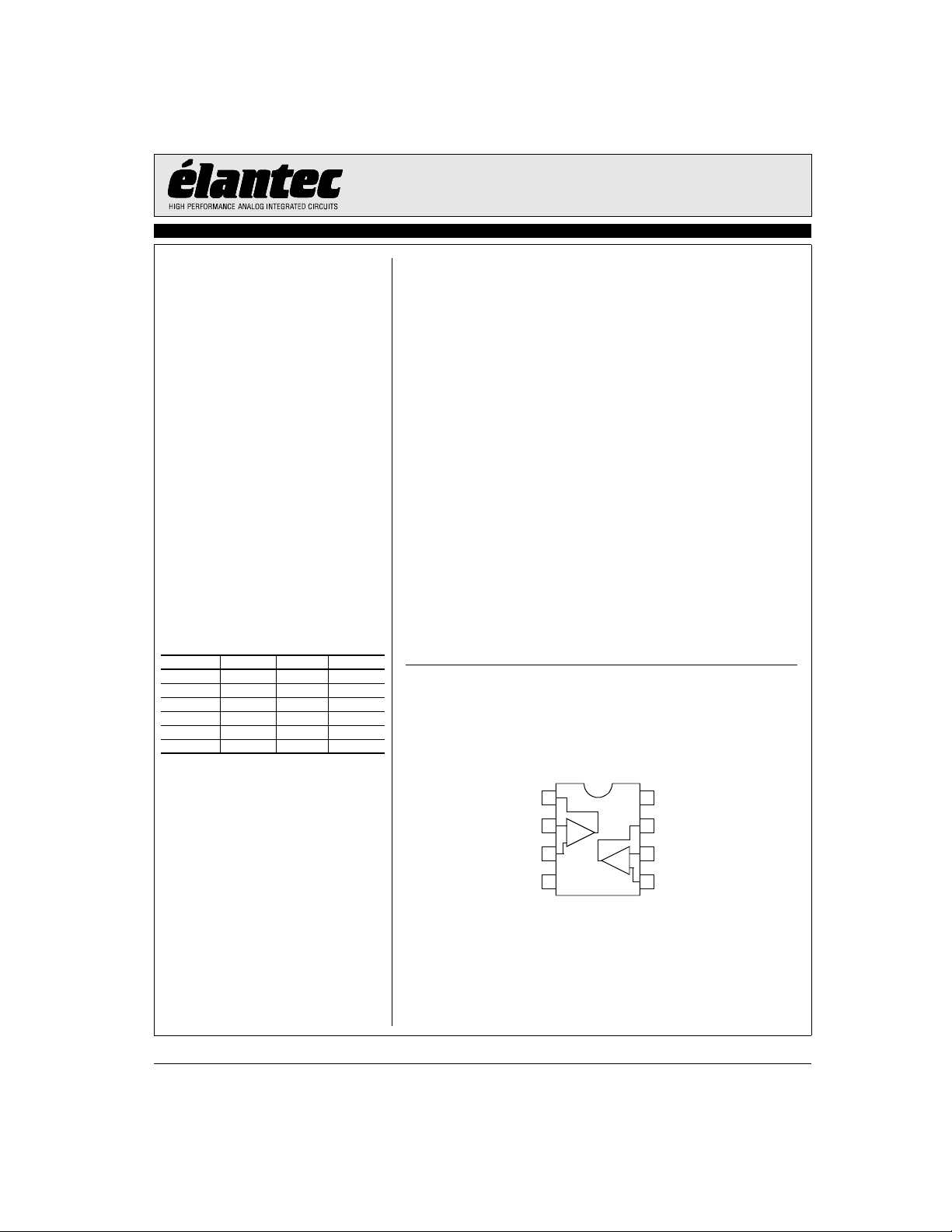
Connection Diagram
1
VOUTA
2
VINA-
VINA+
Note: All information contained in this data sheet has been carefully checked and is believed to be accurate as of the date of publication; however, this data sheet cannot be a “controlled document”. Current revisions, if any, to these
specifications are maintained at the factory and are available upon your request. We recommend checking the revision level before finalization of your design documentation.
© 2001 Elantec Semiconductor, Inc.
+
3
4
VS-
EL2227C
(8-Pin SO and 8-Pin MSOP)
8
VS+
7
VOUTB
65-
VINB-
+
VINB+
August 3, 2001
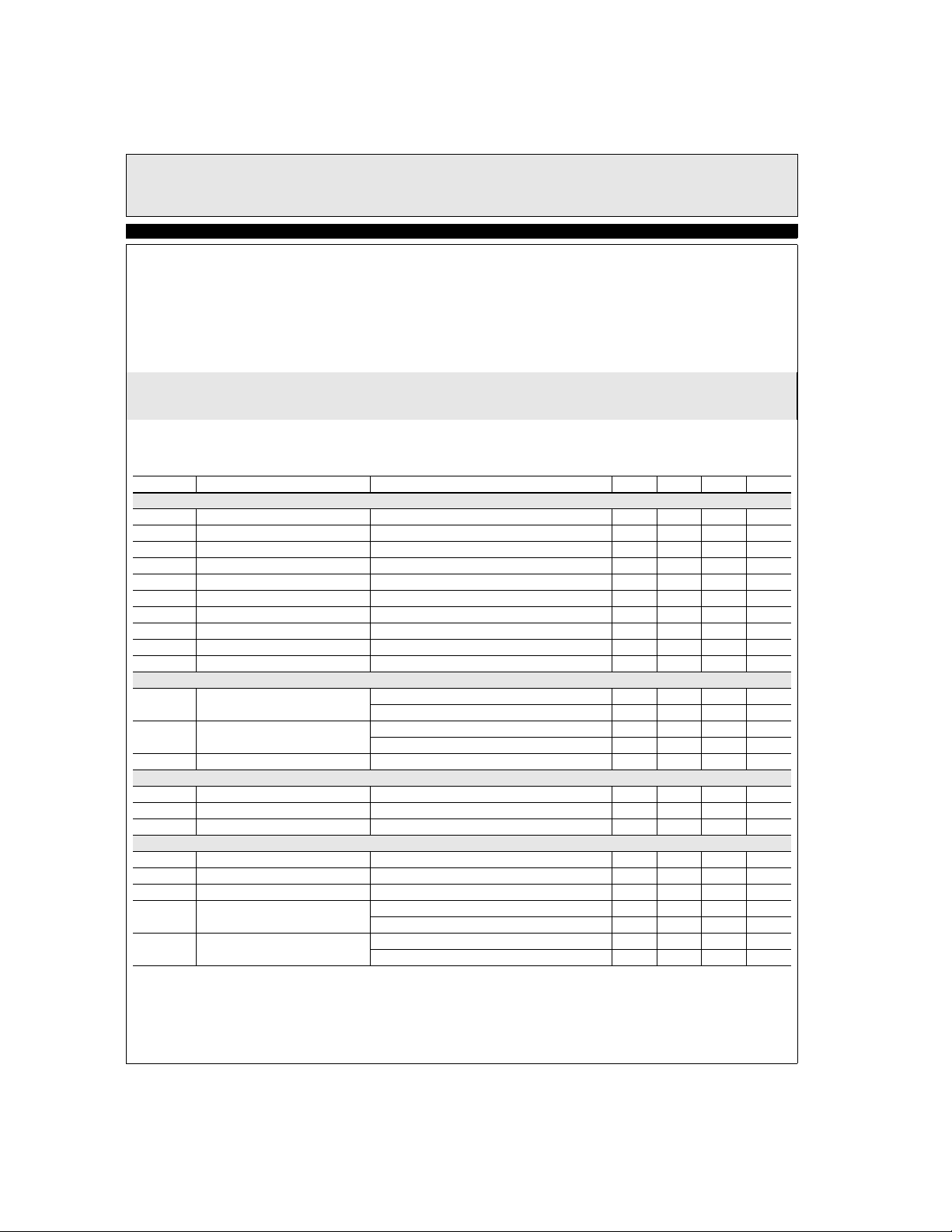
EL2227C
Dual Very Low Noise Amplifier
EL2227C
Absolute Maximum Ratings (T
Values beyond absolute maximum ratings can cause the device to be prematurely damaged. Absolute maximum ratings are stress ratings only
and functional device operation is not implied
Supply Voltage between VS+ and VS- 28V
Input Voltage VS- - 0.3V, VS +0.3V
Maximum Continuous Output Current 40mA
Important Note:
All parameters having Min/Max specifications are guaranteed. Typ values are for information purposes only. Unless otherwise noted, all tests are at the
specified temperature and are pulsed tests, therefore: TJ = TC = TA.
= 25°C)
A
Maximum Die Temperature 150°C
Storage Temperature -65°C to +150°C
Operating Temperature -40°C to +85°C
Power Dissipation See Curves
ESD Voltage 2kV
Electrical Characteristics
VS+ = +12V, VS - = -12V, RL = 500Ω and CL = 3pF to 0V, RF = RG = 620Ω, and TA = 25°C unless otherwise specified.
Parameter Description Condition Min Typ Max Unit
Input Characteristics
V
OS
TCV
I
B
R
IN
C
IN
CMIR Common-Mode Input Range -11.8 +10.4 V
CMRR Common-Mode Rejection Ratio for VIN from -11.8V to 10.4V 60 94 dB
A
VOL
e
n
i
n
Output Characteristics
V
OL
V
OH
I
SC
Power Supply Performance
PSRR Power Supply Rejection Ratio VS is moved from ±2.25V to ±12V 65 95 dB
I
S
V
S
Dynamic Performance
SR Slew Rate
t
S
BW -3dB Bandwidth RF = 358Ω 115 MHz
HD2 2nd Harmonic Distortion f = 1MHz, VO = 2V
HD3 3rd Harmonic Distortion f = 1MHz, VO = 2V
Input Offset Voltage V
Average Offset Voltage Drift
OS
Input Bias Current V
Input Impedance 7.3 MΩ
Input Capacitance 1.6 pF
Open-Loop Gain -5V ≤ V
Voltage Noise f = 100kHz 1.9 nV/√Hz
Current Noise f = 100kHz 1.2 pA/√Hz
Output Swing Low RL = 500Ω -10.4 -10 V
Output Swing High RL = 500Ω 10 10.4 V
Short Circuit Current RL = 10Ω 140 180 mA
Supply Current (Per Amplifier) No Load 4.8 6.5 mA
Operating Range ±2.5 ±12 V
[2]
Settling to 0.1% (AV = +2) (AV = +2), V
= 0V -0.2 3 mV
CM
[1]
= 0V -9 -3.4 µA
CM
≤ 5V 70 87 dB
OUT
RL = 250Ω -9.8 -9 V
RL = 250Ω 9.5 10 V
±2.5V square wave, measured 25%-75% 40 50 V/µS
±1V 65 ns
O =
, RL = 500Ω, RF = 358Ω 93 dBc
f = 1MHz, VO = 2V
f = 1MHz, VO = 2V
P-P
, RL = 150Ω, RF = 358Ω 83 dBc
P-P
, RL = 500Ω, RF = 358Ω 94 dBc
P-P
, RL = 150Ω, RF = 358Ω 76 dBc
P-P
-0.6 µV/°C
2
EL2227C
Dual Very Low Noise Amplifier
Electrical Characteristics
VS+= +5V, VS - = -5V, RL = 500Ω and CL = 3pF to 0V, RF = 620Ω & TA = 25°C unless otherwise specified.
Parameter Description Condition Min Typ Max Unit
Input Characteristics
V
OS
TCV
I
B
R
IN
C
IN
CMIR Common-Mode Input Range -4.8 3.4 V
CMRR Common-Mode Rejection Ratio for VIN from -4.8V to 3.4V 60 97 dB
A
VOL
e
n
i
n
Output Characteristics
V
OL
V
OH
I
SC
Power Supply Performance
PSRR Power Supply Rejection Ratio VS is moved from ±2.25V to ±12V 65 95 dB
I
S
V
S
Dynamic Performance
SR Slew Rate
t
S
BW -3dB Bandwidth RF = 358Ω 90 MHz
HD2 2nd Harmonic Distortion f = 1MHz, VO = 2V
HD3 3rd Harmonic Distortion f = 1MHz, VO = 2V
Input Offset Voltage V
Average Offset Voltage Drift
OS
Input Bias Current V
= 0V 0.2 3 mV
CM
[1]
= 0V -9 -3.7 µA
CM
-0.6 µV/°C
Input Impedance 7.3 MΩ
Input Capacitance 1.6 pF
Open-Loop Gain -5V ≤ V
≤ 5V 70 84 dB
OUT
Voltage Noise f = 100kHz 1.9 nV/√Hz
Current Noise f = 100kHz 1.2 pA/√Hz
Output Swing Low RL = 500Ω -3.8 -3.5 V
RL = 250Ω -3.7 -3.5 V
Output Swing High RL = 500Ω 3.5 3.7 V
RL = 250Ω 3.5 3.6 V
Short Circuit Current RL = 10Ω 60 100 mA
Supply Current (Per Amplifier) No Load 4.5 5.5 mA
Operating Range ±2.5 ±12 V
[2]
Settling to 0.1% (AV = +2) (AV = +2), V
±2.5V square wave, measured 25%-75% 35 45 V/µS
±1V 77 ns
O =
, RL = 500Ω, RF = 358Ω 98 dBc
P-P
f = 1MHz, VO = 2V
f = 1MHz, VO = 2V
, RL = 150Ω, RF = 358Ω 90 dBc
P-P
, RL = 500Ω, RF = 358Ω 94 dBc
P-P
, RL = 150Ω, RF = 358Ω 79 dBc
P-P
EL2227C
3
EL2227C
Dual Very Low Noise Amplifier
EL2227C
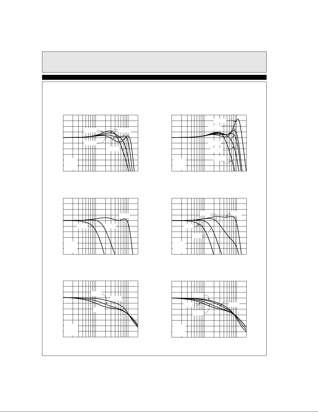
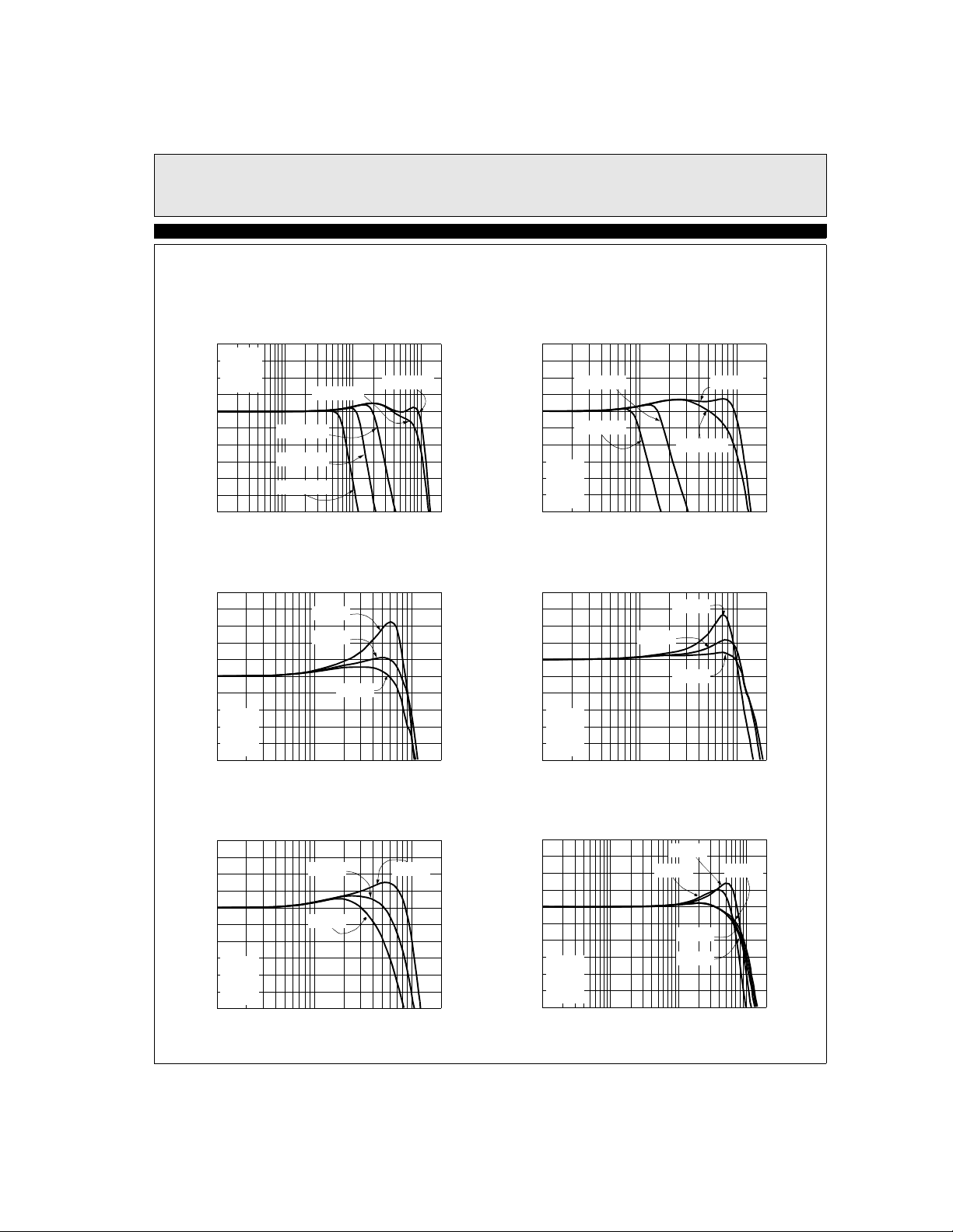
Typical Performance Curves
Non-inverting Frequency Response for Various R
4
3
2
1
0
-1
-2
-3
Normalized Gain (dB)
-4
VS=±12V
AV=+2
-5
RL=500Ω
-6
1M 10M 100M
Non-inverting Frequency Response (Gain)
4
3
2
1
0
-1
-2
-3
Normalized Gain (dB)
-4
VS=±12V
RF=350Ω
-5
RL=500Ω
-6
1M 10M 100M
RF=1kΩ
RF=100Ω
RF=350Ω
Frequency (Hz)
AV=5AV=10 AV=-10
Frequency (Hz)
RF=620Ω
AV=2
F
200M
200M
Inverting Frequency Response for Various R
4
3
2
1
0
-1
-2
-3
Normalized Gain (dB)
-4
VS=±12V
AV=-1
-5
RL=500Ω
-6
1M 10M 100M
Inverting Frequency Response (Gain)
4
3
2
1
0
-1
-2
-3
Normalized Gain (dB)
-4
VS=±12V
RF=420Ω
-5
RL=500Ω
-6
1M 10M 100M
AV=-5
RF=100Ω
RF=350Ω
RF=420Ω
RF=620Ω
RF=1kΩ
Frequency (Hz)
AV=-2 AV=-1
Frequency (Hz)
F
200M
200M
Non-inverting Frequency Response (Phase)
135
90
45
0
-45
-90
Phase (°)
-135
-180
-225
VS=±12
RF=350Ω
-270
RL=500Ω
-315
1M 10M
AV=5
AV=10
Frequency (Hz)
AV=2
100M 200M
Inverting Frequency Response (Phase)
135
90
45
0
-45
-90
Phase (°)
-135
-180
-225
VS=±12V
RF=420Ω
-270
RL=500Ω
-315
1M 10M 100M
AV=-10
AV=-1
AV=-2
AV=-5
200M
Frequency (Hz)
4
Typical Performance Curves
EL2227C
EL2227C
Dual Very Low Noise Amplifier
Non-inverting Frequency Response for Various
Input Signal Levels
4
VS=±12V
3
RF=350Ω
AV=+2
2
RL=500Ω
1
0
-1
-2
-3
Normalized Gain (dB)
-4
-5
-6
100k 1M 10M
Non-inverting Frequency Response for Various C
5
4
3
2
1
0
-1
-2
Normalized Gain (dB)
VS=±12V
RF=620Ω
-3
RL=500Ω
-4
AV=+2
-5
1M 10M 100M
VIN=500mV
VIN=1V
VIN=2V
Frequency (Hz)
Frequency (Hz)
VIN=100mV
PP
PP
PP
CL=30pF
CL=12pF
PP
CL=2pF
VIN=20mV
100M
Inverting Frequency Response for Various Input
Signal Levels
4
3
2
PP
-1
-2
-3
Normalized Gain (dB)
-4
-5
-6
L
-1
-2
-3
Normalized Gain (dB)
-4
-5
200M
-6
VIN=1.4V
VIN=2.8V
PP
PP
Frequency (Hz)
CL=12pF
Frequency (Hz)
1
0
VS=±12V
RF=420Ω
RL=500Ω
AV=-1
1M 10M 100M
Inverting Frequency Response for Various C
4
3
2
1
0
VS=±12V
RF=420Ω
RL=500Ω
AV=-1
1M 10M 100M
VIN=280mV
CL=30pF
CL=2pF
VIN=20mV
PP
PP
200M
L
200M
Non-inverting Frequency Response for Various R
4
3
2
1
0
-1
-2
-3
Normalized Gain (dB)
VS=±12V
RF=620Ω
-4
CL=15pF
-5
AV=+2
-6
1M 10M 100M
RL=100Ω RL=500Ω
RL=50Ω
Frequency (Hz)
L
200M
Frequency Response for Various Output DC
Levels
4
3
2
1
0
-1
-2
-3
Normalized Gain (dB)
VS=±12V
RF=620Ω
-4
RL=500Ω
-5
AV=+2
-6
100k 1M 10M
VO=+10V
VO=-10V VO=+5V
VO=0V
VO=-5V
100M
Frequency (Hz)
5

EL2227C
Dual Very Low Noise Amplifier
EL2227C
Typical Performance Curves
3dB Bandwidth vs Supply Voltage
140
AV=+2
RF=620Ω
120
RL=500Ω
100
80
60
3dB Bandwidth (MHz)
40
AV=+5 AV=-5
20
0
2 4 8
Large Signal Step Response
VS=±12V
0.5V/div
AV=-1
AV=+2
AV=-2
Supply Voltage (±V)
AV=+10
AV=-10
RF=620Ω
AV=2
RL=500Ω
Peaking vs Supply Voltage
4
AV=+2
3.5
3
2.5
AV=-1
2
AV=+10
Peaking (dB)
1.5
AV=-10
1
0.5
0
126 10
2 4 8
Large Signal Step Response
VS=±2.5V
0.5V/div
AV=+5
AV=-5
Supply Voltage (±V)
AV=+2
RF=620Ω
RL=500Ω
AV=-2
RF=620Ω
AV=2
RL=500Ω
126 10
Small Signal Step Response
VS=±12V
20mV/div
100ns/div
100ns/div
RF=620Ω
AV=2
RL=500Ω
6
Small Signal Step Response
VS=±2.5V
20mV/div
100ns/div
100ns/div
RF=620Ω
AV=2
RL=500Ω

Typical Performance Curves
EL2227C
EL2227C
Dual Very Low Noise Amplifier
Group Delay vs Frequency
10
8
6
4
2
0
-2
Group Delay (ns)
-4
-6
-8
-10
1M 10M
Supply Current vs Supply Voltage Closed Loop Output Impedance vs Frequency
12
1.2/div
6
Supply Current (mA)
0
1.2/div
AV=5V
AV=2V
Frequency (Hz)
Supply Voltage (±V)
6 120
VS=±12V
RF=620Ω
RL=500Ω
PIN=-20dBm into 50Ω
100M
Differential Gain/Phase vs DC Input Voltage at
3.58MHz
0.1
0.08
0.06
0.04
dG (%) or dP (°)
0.02
-0.02
Output Impedance (Ω)
0.01
dP
0
-1 0
100
10
1
0.1
10k 1M
-0.5 0.5
DC Input Voltage (V)
100k 10M
Frequency (Hz)
dG
AV=2
RF=620Ω
RL=150Ω
fO=3.58MHz
1
100M
CMRR
110
90
70
50
-CMRR (dB)
30
VS=±12
10
10 10k
Frequency (Hz)
1M 100M100 1k 100k 10M
PSRR
0
20
40
PSRR (dB)
60
80
100
1k 1M
VS-
100k
Frequency (Hz)
VS+
10M 100M10k
7

EL2227C
Dual Very Low Noise Amplifier
EL2227C
Typical Performance Curves
1MHz 2nd and 3rd Harmonic Distortion vs Output
Swing for VS=±12V
-40
AV=2
RF=620Ω
-50
RL=500Ω
-60
-70
Distortion (dBc)
-80
-90
-100
0 8
Total Harmonic Distortion vs Frequency @ 2V
VS=±12V
-60
-70
-80
-90
THD (dBc)
-100
-110
-120
1
2nd H
3rd H
12
Output Swing (VPP)
RL=50
RL=500
Frequency (kHz)
1MHz 2nd and 3rd Harmonic Distortion vs Output
Swing for VS=±2.5V
-50
AV=2
RF=358Ω
RL=500Ω
-60
-70
-80
Distortion (dBc)
-90
16 204
PP
100010 100
-100
0 1.5
Total Harmonic Distortion vs Frequency @ 2V
VS=±2.5V
-60
-70
-80
-90
THD (dBc)
-100
-110
-120
1 100010 100
2nd H
3rd H
2.50.5 21
Output Swing (VPP)
PP
RL=50
RL=500
Frequency (kHz)
Voltage and Current Noise vs Frequency
10
9
8
7
I
N
6
5
4
3
2
Voltage Noise (nV/√Hz), Current Noise (pA/√Hz)
1
10 1k
E
N
Frequency (Hz)
Channel to Channel Isolation vs Frequency
0
-20
-40
Gain (dB)
-60
-80
10k 100k100
-100
100k 1M
Frequency (Hz)
A → B
B → A
100M10M
8

Typical Performance Curves
EL2227C
EL2227C
Dual Very Low Noise Amplifier
-3dB Bandwidth vs Temperature
150
140
130
120
110
-3dB Bandwidth (MHz)
100
90
80
2
0
(mV)
OS
V
-2
-4
-50 0
0 100
V
vs Temperature
OS
40-20-40 20 80 14060 120
Die Temperature (°C)
Die Temperature (°C)
100
Supply Current vs Temperature
10
9.5
(mA)
S
I
9
8.5
-50 50
Die Temperature (°C)
Input Bias Current vs Temperature
-2
-3
(µA)
-4
BIAS
I
-5
15050
-6
-50 50
Die Temperature (°C)
100 1500
100 1500
Slew Rate vs Temperature
55
53
51
49
Slew Rate (V/µs)
47
45
-50
50 1500 100
Die Temperature (°C)
Settling Time vs Accuracy
160
140
120
100
80
60
Settling Time (ns)
40
20
0
0.01
VS=±2.5V
VO=2V
VS=±12V
VO=2V
PP
PP
Accuracy (%)
VS=±12V
VO=5V
PP
10.1
9

EL2227C
Dual Very Low Noise Amplifier
EL2227C
Typical Performance Curves
Package Power Dissipation vs Ambient Temp.
JEDEC JESD51-3 Low Effective Thermal Conductivity Test Board
0.9
781mW
0.8
0.7
607mW
0.6
0.5
0.4
0.3
Power Dissipation (W)
0.2
0.1
0
0 100
S
θ
O
J
A
8
=
1
6
0
°
C
/
W
M
S
O
θ
P
J
A
8
=
2
0
6
°
C
/
W
Ambient Temperature (°C)
85
15025 1257550
10

Pin Descriptions
EL2227CY
8-Pin MSOP
EL2227CS
8-Pin SO Pin Name Pin Function Equivalent Circuit
1 1 VOUTA Output
2 2 VINA- Input
EL2227C
Dual Very Low Noise Amplifier
VS+
V
OUT
Circuit 1
VS+
EL2227C
3 3 VINA+ Input Reference Circuit 2
4 4 VS- Supply
5 5 VINB+ Input
6 6 VINB- Input Reference Circuit 2
7 7 VOUTB Output Reference Circuit 1
8 8 VS+ Supply
11
VIN-VIN+
VS-
Circuit 2

EL2227C
Dual Very Low Noise Amplifier
EL2227C
Applications Information
Product Description
The EL2227C is a dual voltage feedback operational
amplifier designed especially for DMT ADSL and other
applications requiring very low voltage and current
noise. It also features low distortion while drawing moderately low supply current and is built on Elantec's
proprietary high-speed complementary bipolar process.
The EL2227C use a classical voltage-feedback topology
which allows them to be used in a variety of applications
where current-feedback amplifiers are not appropriate
because of restrictions placed upon the feedback element used with the amplifier. The conventional topology
of the EL2227C allows, for example, a capacitor to be
placed in the feedback path, making it an excellent
Driver
Input
Receive
Out +
Receive
Out -
R
G
Receive
Amplifiers
+
R
F
R
F
-
+
R
F
-
+
+
-
R
F
choice for applications such as active filters, sampleand-holds, or integrators.
ADSL CPE Applications
The low noise EL2227C amplifier is specifically
designed for the dual differential receiver amplifier
function with ADSL transceiver hybrids as well as other
low-noise amplifier applications. A typical ADSL CPE
line interface circuit is shown in Figure 1. The EL2227C
is used in receiving DMT down stream signal. With
careful transceiver hybrid design and the EL2227C
1.9nV/√Hz voltage noise and 1.2pA/√Hz current noise
performance, -140dBm/Hz system background noise
performance can be easily achieved.
R
OUT
R
OUT
R
R
IN
R
R
IN
Line +
Line -
Z
LINE
Figure 1. Typical Line Interface Connection
12

EL2227C
Dual Very Low Noise Amplifier
EL2227C
Disable Function
The EL2227C is in the standard dual amplifier package
without the enable/disable function. A simple way to
implement the enable/disable function is depicted
below. When disabled, both the positive and negative
supply voltages are disconnected (see Figure 2 below.)
+12V
1k
10k
10k
1k
+
-
1k
75k
1µF
1µF 4.7µF
Power Dissipation
With the wide power supply range and large output drive
capability of the EL2227C, it is possible to exceed the
150°C maximum junction temperatures under certain
load and power-supply conditions. It is therefore important to calculate the maximum junction temperature
(T
) for all applications to determine if power sup-
JMAX
ply voltages, load conditions, or package type need to be
modified for the EL2227C to remain in the safe operating area. These parameters are related as follows:
T
JMAXTMAXθJAPDMAXTOTAL
where:
PD
MAXTOTAL
is the sum of the maximum power dissi-
pation of each amplifier in the package (PD
PD
for each amplifier can be calculated as follows:
MAX
PD
MAX
2VSI
SMAXVS
where:
T
=Maximum Ambient Temperature
MAX
×()+=
( V
OUTMAX
V
)
×–+××=
----------------------------
)
MAX
OUTMAX
R
L
θJA =Thermal Resistance of the Package
PD
=Maximum Power Dissipation of 1Amplifier
MAX
VS =Supply Voltage
I
=Maximum Supply Current of 1 Amplifier
MAX
V
OUTMAX
=Maximum Output Voltage Swing of the
Application
RL =Load Resistance
To serve as a guide for the user, we can calculate maximum allowable supply voltages for the example of the
video cable-driver below since we know that T
150°C, T
MAX
= 75°C, I
= 9.5mA, and the package
SMAX
JMAX
=
θJAs are shown in Table 1. If we assume (for this exam-
ple) that we are driving a back-terminated video cable,
then the maximum average value (over duty-cycle) of
V
OUTMAX
is 1.4V, and RL = 150Ω, giving the results
seen in Table 1.
Table 1
Part Package θ
EL2227CS SO8 160°C/W 0.406W @ 85°C
EL2227CY MSOP8 206°C/W 0.315W @ 85°C
Max PD
JA
Single-Supply Operation
The EL2227C have been designed to have a wide input
and output voltage range. This design also makes the
EL2227C an excellent choice for single-supply operation. Using a single positive supply, the lower input
voltage range is within 200mV of ground (RL = 500Ω),
and the lower output voltage range is within 875mV of
ground. Upper input voltage range reaches 3.6V, and
output voltage range reaches 3.8V with a 5V supply and
RL = 500Ω. This results in a 2.625V output swing on a
single 5V supply. This wide output voltage range also
allows single-supply operation with a supply voltage as
high as 28V.
Gain-Bandwidth Product and the -3dB
Bandwidth
The EL2227C have a gain-bandwidth product of
137MHz while using only 5mA of supply current per
amplifier. For gains greater than 2, their closed-loop ----
-3dB bandwidth is approximately equal to the gain-
@
ISS
T
MAX
Max V
S
13

EL2227C
Dual Very Low Noise Amplifier
EL2227C
bandwidth product divided by the noise gain of the circuit. For gains less than 2, higher-order poles in the
amplifiers' transfer function contribute to even higher
closed loop bandwidths. For example, the EL2227C
have a -3dB bandwidth of 115MHz at a gain of +2, dropping to 28MHz at a gain of +5. It is important to note
that the EL2227C have been designed so that this
“extra” bandwidth in low-gain applications does not
come at the expense of stability. As seen in the typical
performance curves, the EL2227C in a gain of +2 only
exhibit 0.5dB of peaking with a 1000Ω load.
Output Drive Capability
The EL2227C have been designed to drive low impedance loads. They can easily drive 6VPP into a 500Ω load.
This high output drive capability makes the EL2227C an
ideal choice for RF, IF and video applications.
Printed-Circuit Layout
The EL2227C are well behaved, and easy to apply in
most applications. However, a few simple techniques
will help assure rapid, high quality results. As with any
high-frequency device, good PCB layout is necessary
for optimum performance. Ground-plane construction is
highly recommended, as is good power supply bypassing. A 0.1µF ceramic capacitor is recommended for
bypassing both supplies. Lead lengths should be as short
as possible, and bypass capacitors should be as close to
the device pins as possible. For good AC performance,
parasitic capacitances should be kept to a minimum at
both inputs and at the output. Resistor values should be
kept under 5kΩ because of the RC time constants associated with the parasitic capacitance. Metal-film and
carbon resistors are both acceptable, use of wire-wound
resistors is not recommended because of their parasitic
inductance. Similarly, capacitors should be low-inductance for best performance.
14

EL2227C
Dual Very Low Noise Amplifier
EL2227C
General Disclaimer
Specifications contained in this data sheet are in effect as of the publication date shown. Elantec Semiconductor, Inc. reserves the right to make
changes in the circuitry or specifications contained herein at any time without notice. Elantec Semiconductor, Inc. assumes no responsibility for
the use of any circuits described herein and makes no representations that they are free from patent infringement.
WARNING - Life Support Policy
Elantec Semiconductor, Inc. products are not authorized for and should
not be used within Life Support Systems without the specific written con-
Elantec Semiconductor, Inc.
675 Trade Zone Blvd.
Milpitas, CA 95035
Telephone: (408) 945-1323
(888) ELANTEC
Fax: (408) 945-9305
European Office: +44-118-977-6020
Japan Technical Center: +81-45-682-5820
sent of Elantec Semiconductor, Inc. Life Support systems are equipment
intended to support or sustain life and whose failure to perform when
properly used in accordance with instructions provided can be reasonably
expected to result in significant personal injury or death. Users contemplating application of Elantec Semiconductor, Inc. Products in Life
Support Systems are requested to contact Elantec Semiconductor, Inc. factory headquarters to establish suitable terms & conditions for these
applications. Elantec Semiconductor, Inc.’s warranty is limited to replacement of defective components and does not cover injury to persons or
property or other consequential damages.
August 3, 2001
15
Printed in U.S.A.
 Loading...