

Page 1

SERVICE MANUAL
5
CHANNEL I CHANNEL II
4
6
3
2
1
3
2
1
7
PROTECT
8
CLIP
9
SIGNAL
BRIDGED
100
5
CHANNEL I CHANNEL II
4
6
THERMAL
7 3
PROTECT
8
CLIP
9
SIGNAL
0
BRIDGED
10
5
4
6
THERMALTHERMAL
3
2
1
2
1
7
PROTECT
8
CLIP
9
0
5
4
0
SIGNAL
10
6
THERMAL
7
PROTECT
8
CLIP
9
SIGNAL
10
OFF
ON
OFF
ON
SWITCHING POWER MOSFET AMPLIFIER
SWITCHING POWER MOSFET AMPLIFIER
Page 2

SERVICE MANUAL PAM6100 / 4100
INDEX
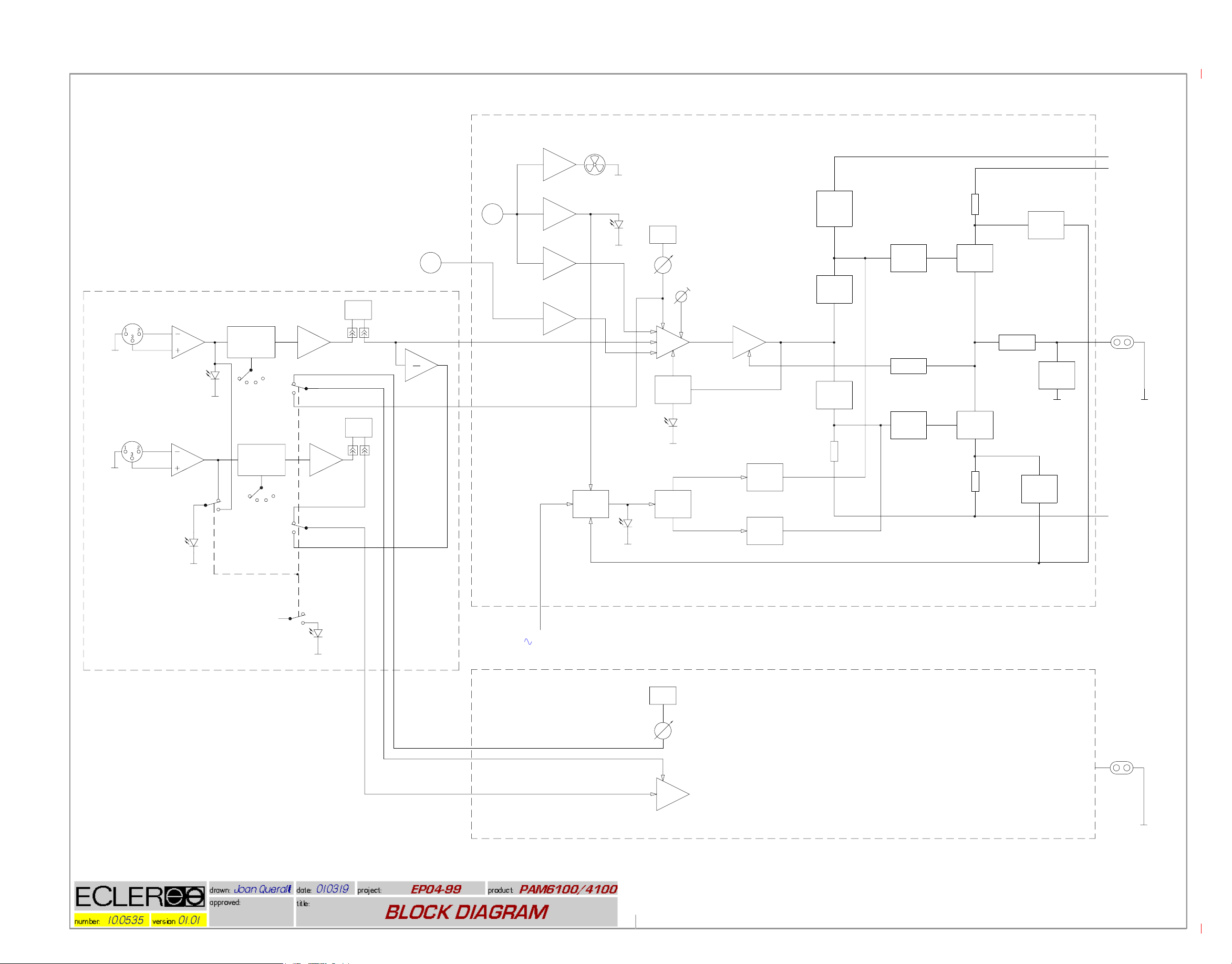
PAM6100
- BLOCK DIAGRAM
- FUNCTIONING DESCRIPTION
SCHEMATICS
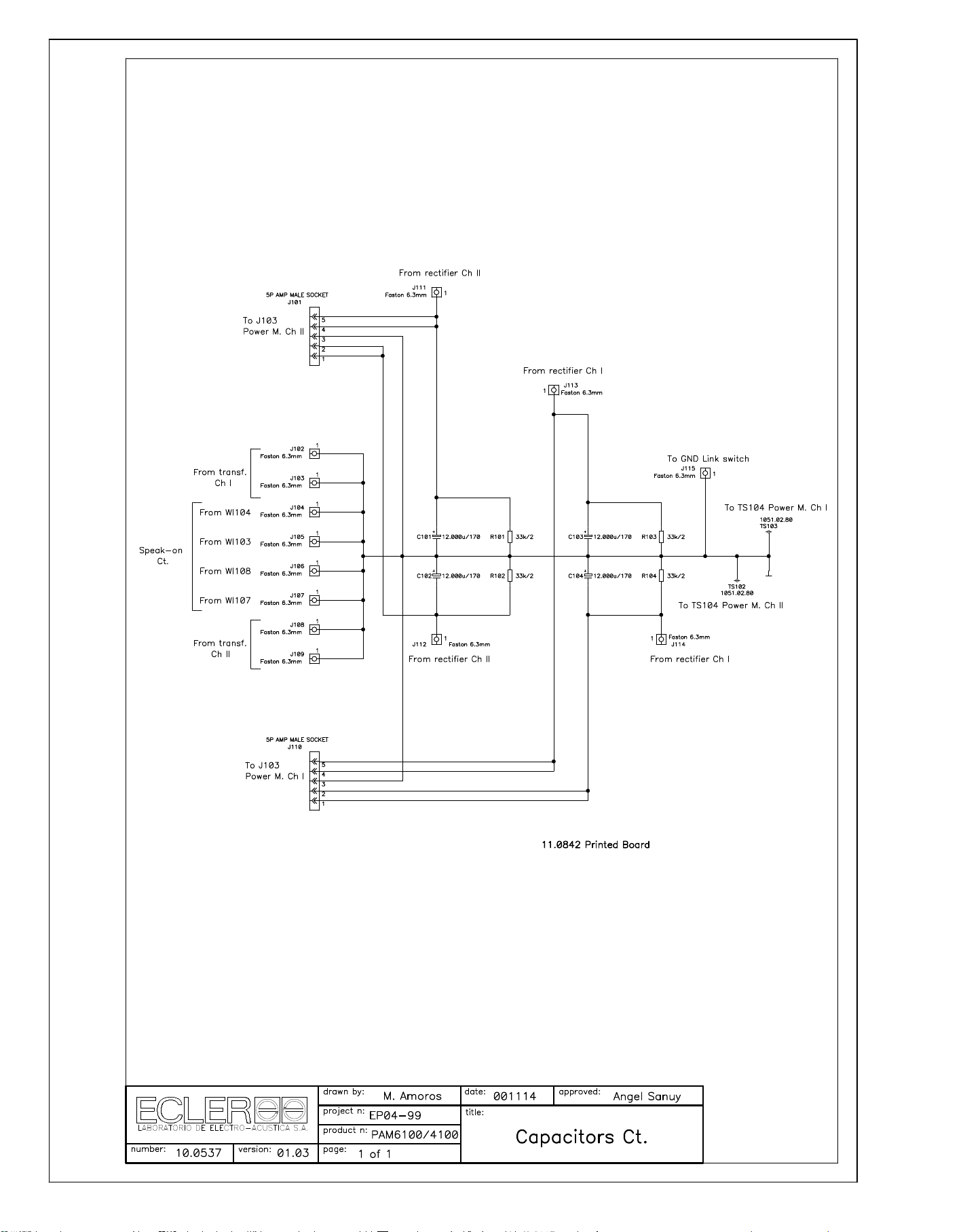
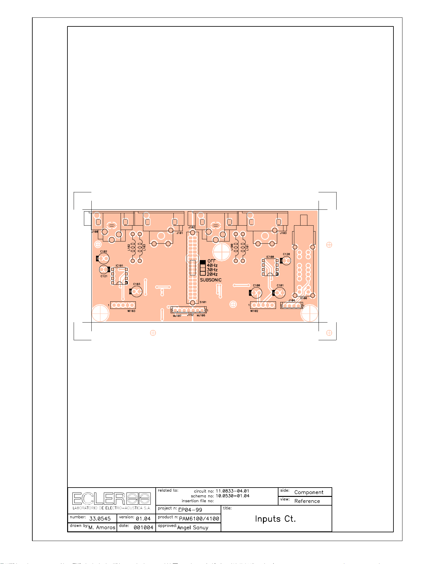
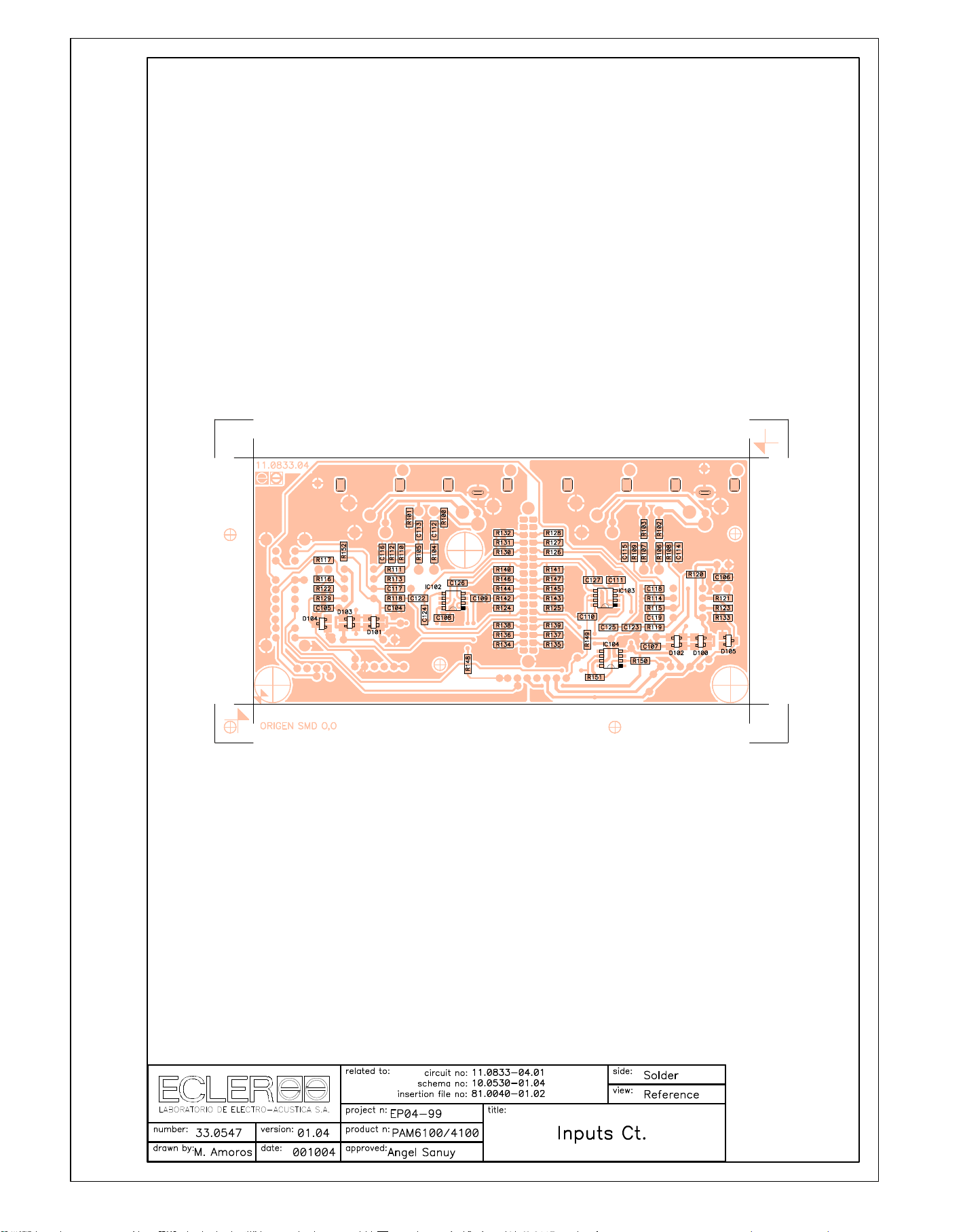
Inputs circuit
Power Amplifier circuit
Soft-Start Power Supply circuit
Potentiometers and leds circuit
Capacitors circuit
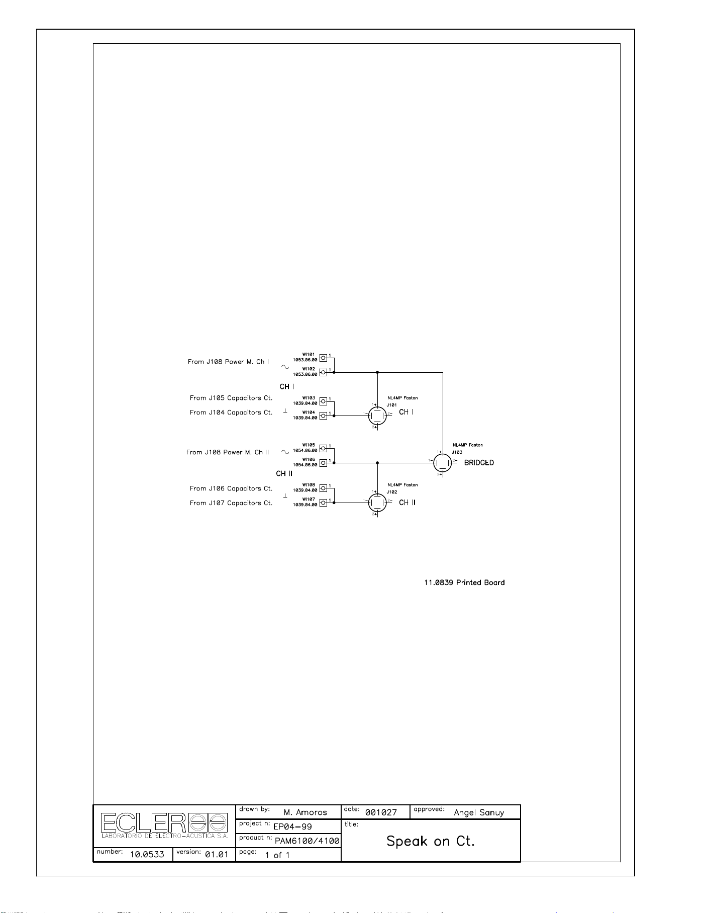
Speak on circuit
- COMPONENTS LOCATION SCHEMA
AND PARTS LIST
Inputs circuit
Power Amplifier circuit
Soft-Start Power Supply circuit
Potentiometers and leds circuit
Capacitors circuit
Speak on circuit
- TESTING AND QUALITY CONTROL
- TECHNICAL CHARACTERISTICS
- WIRING DIAGRAM
- MECHANICAL DIAGRAM
- PACKING DIAGRAM
PAM4100
- COMPONENTS LOCATION SCHEMA
AND PARTS LIST
Power Amplifier circuit
- MECHANICAL DIAGRAM
Page 3
CH 1
OPTIONAL
MODULES
TRANSFORMER
THERMAL
PROBE
MODULE
THERMAL
PROBE
FAN CONTROL
THERMAL PROTECT
THERMAL PROCESSOR
THERMAL PROCESSOR
FAN
++Vcc
+Vcc
WILSON
CURRENT
THERMAL
-Vref
VOLUME
MIRROR
DRIVER MOSFET N
LEVEL
CONVERTER
ADJ 0dB
OVERLOAD
HIGH SIDE
CH 2
INPUT CIRCUIT
HIGH PASS FILTER
STEREO
S.P.
OFF
20Hz
30Hz
40Hz
HIGH PASS FILTER
S.P.
BRIG
OPTIONAL
MODULES
PROTECTION
20Hz
OFF
40Hz
30Hz
AND TIMER
PROTECT
VCA
ANTICLIP
CONTROL
RELAY
CONTROL
FEEDBACK
LEVEL
CONVERTER
DRIVER MOSFET N
CLIP
OUTPUT
SHUTDOWN
OUTPUT
SHUTDOWN
ZOBEL
OUT 1
DC PROTECT
CROWBAR
OVERLOAD
LOW SIDE
-Vcc
POWER MODUL CIRCUIT
+15V
BRIG
AC DETECT
-Vref
VOLUME
OUT 2
VCA
POWER MODUL CIRCUIT
Page 4

author: Queralt date: 010418 project:
C
E
num:
EPO4-99 Power Module. Functioning description.
structure differs from the design used untill now. This is due to the breakdown voltage
limit on P-channel MosFET's, wich is 200V. This final stage is formed by several
shunted MosFET's, where those of the positive branch are common-drain configured,
and the negative branch are mounted in common-source configuration.
internally compensated in order to obtain gain levels equal or higher than three. The
amplifier's feedback is given by a resistor and a capacitor associated to the operational
amplifier's non inverting input.
Transistors BF587 and BF588 are common-base configured, forming a current supply
structure. This specific transistor type is used because of the higher Vce voltage level
required by this design. They perform simultaneously two functions: they polarize the
MosFET's gate-source junctions, keeping them on the conducting edge, and they
tranfer the OpAmp's output voltage variations referred to signal ground.
LER
52.0010 version: 01.00
Due to the high power level required on the output load, the amplifier final stage's
The system's controlling device is a NE5534-type operational amplifier, wich is
approved:
title:
FUNCTIONING DESCRIPTION
EP04-99
product:
PAM4/6100
The signal variations normally reflected by Q107 and referred to the positive power
supply, are now needed to be floating variations, and referred to the outputs. This
function is done by Q109-110 (BF588), wich are mounted formig a Wilson-type mirror
current supply. This mirror current supply transfers all of the current variations detected
while descending through Q109's collector, to similar variations on Q110's collector
also downward current. Resistors R167 and R174 are used to balance the current
mirror, in order to avoid the use of transistors with forcibly the same beta value. C138
and C141 suppress their resistance when high frequency signal is processed. Diodes
D126 and D127 avoid the transistors to get saturated, and R171 eliminates the loads
on BF588's bases (Baker Circuit).
The system requires about 12Vdc additional voltage upon the usual Vcc level, this
allows a correct saturation and a symetric clipping at the higher MosFET's.
The correct polarization current value is adjusted by a 4K7 potentiometer connected to
the BF transistor's emitter. This adds an additional current to the current source output
on th BF transistor's loading resistors.
In order to maintain the appropiate stand-by current level against varying temperature
conditions, BD437-type transistors are used. As they have a particular temperaturedepending base-emitter voltage curve, this voltage is used to keep a correct voltage
reference for the current supply. As the temperature rises, the reference voltage level
decreases, the gate-source voltage also decreases and, finally, the bias current also
decreases.
52-0010-0100 EP04-99 Anglès.xls 1 of 3
Page 5

Transistors Q111 and Q112, and their corresponding twins at the lower branch, form
Stand-
a current-buffering circuit wich allows a fast charge and discharge of the power
MosFET's gates.
The Zobel circuit, a resistance-capacitance-inductance formed network associated to
the amplifier's ouput, tries to keep the amplifier's output load impedance constant no
matter wich load value is conected to the output, or wich frequency is processed, in
order to avoid phase shifts on the feedback signal.
To avoid the presence of DC voltage on the output, a diac-triac based system is used,
wich shorts the output to signal ground in case the DC level reaches the diac's
triggering value. To avoid this to happen when processing correct signal (sine
waveform, music...), the diac obtains its reference level from a filtering network formed
by a 100K resistor and a 1mF capacitor.
The protections circuitry overhauls the MosFET's power consumption. Basically, this
circuitry consists of two important sections: MosFET's Id current monitoring, and
MosFET's Vds value detection.
When the MosFET's Id level rises above a certain level, transistor Q119 (controlling
transistor) conducts and decreases the BF transistor's loading resistance, thus reducing
also their gate-source voltage and, finally, lowering the Id current value. This system is
helped by a delayed performance, due to the associated circuitry to Q145 and C174.
This capacitor starts to charge when a current level above the allowed value is
detected, and the protection starts. The greater is the capacitor's charge level, the
higher is also the voltage applied to Q119 controlling transistor's base, increasing its
conduction and, consequently, reducing the gate-source voltage and thus the Id current
value. This system uses a feedback network. The delay used is necessary to avoid
clipping the processed signal's dynamic range, wich should result in the typical clipping
noise. In the negative branch, the protection circuitry is associated to control transistor
Q120.
In case the overcurrent is not ocassional, and persists, after a period of time between
4 and 10 seconds (determined by R142 and C124), the system switches back to
by mode, due to a system-reset. This is done by an optocoupler (IC113) associated to
the negative branch protection circuitry. When protections get activated, IC113
gradually charges C124 untill a 40106-type Schmidt trigger gate switches over . If the
problem persists, this cycle is repeated.
STANDBY CIRCUITRY.
This circuit maintains the Output shutdown relay closed for about 10 seconds, and
thus annulates any current through the MosFET's during this period, just untill the
whole system's power supply voltage reaches its stable level. By this system, we avoid
to hear through the loudspeakers any possible annoying noise proceeding from the
system's start-up.
52-0010-0100 EP04-99 Anglès.xls 2 of 3
Page 6

This delay time is achieved by using a RC cell, where R135=287K and
40106-
C119=47mF/50V. As this cell charges, its voltage increases untill reaching the
type Schmidt trigger (IC108) switching value; at this point, the relay opens and the
amplifier starts to function normally.
The discharge or reset of capacitor C119=47mF can be done by cutting off the power
supply, or by triggering the Thermal or other protections. During a short period of time,
BC817-type transistor Q102 acts like a switch, shunting two 750 ohm resistors to
C119.
Moreover, the amplifier includes some other additional features, like:
· Volume control by a VCA system.
· An ANTICLIP system.
· A Temperature control system.
The ANTICLIP system. When the amplifier reaches clipping levels, the operational
amplifier looses control on the system's performance and at its output some ±Vcc
voltage peaking pulses may appear, proceeding from its power supply. This peaking
pulses are used to be rectified and sent to an optocoupler (IC111), wich varies the
system's VCA control voltage as a function of those pulse's amplitude, creating a
negative feedback wich should pull back the system into stable functioning area.
The Temperature control system has three main functions:
· Controlling the cooling fan speed, as it is a function of the measured temperature. The
fan's operation voltage range is »7 to 4 Volt.
· Suspending the amplifier's functioning when the temperature exceeds »92ºC
· Reducing the amount of power output, depending on the module's temperature (as it
rises above 85ºC) and on the main power supply's transformer (above 120ºC).
The temperature control system consists on two LM35D-type IC's, wich act like a
thermal probe; one is placed on the amplifier's heat sink, and the other is placed into
the main power supply transformer's core. Moreover, three amplifiers, a comparator
for the thermal probe and a 7805-type IC to feed the cooling fan are used.
The first amplifier (1/4 IC114) acts on the cooling fan speed control. The second
amplifier (1/4 IC114) modifies the VCA gain control, in order to reduce the system's
gain if the temperature rises above 85ºC. The third amplifier (1/4 IC114) modifies the
VCA gain control, in order to reduce the system's gain if the temperature rises above
120ºC. The comparator (1/4 IC114) is responsible for the output shutdown relay
performance, in order to close it as the temperature reaches 92ºC, and thus cutting of
the amplifier's MosFETs bias current. As this happens, the signal output of the whole
unit is cutted off.
52-0010-0100 EP04-99 Anglès.xls 3 of 3
Page 7

Page 8

Page 9
Page 10
Page 11
Page 12
Page 13
Page 14
Page 15

Page 16
Page 17

Page 18

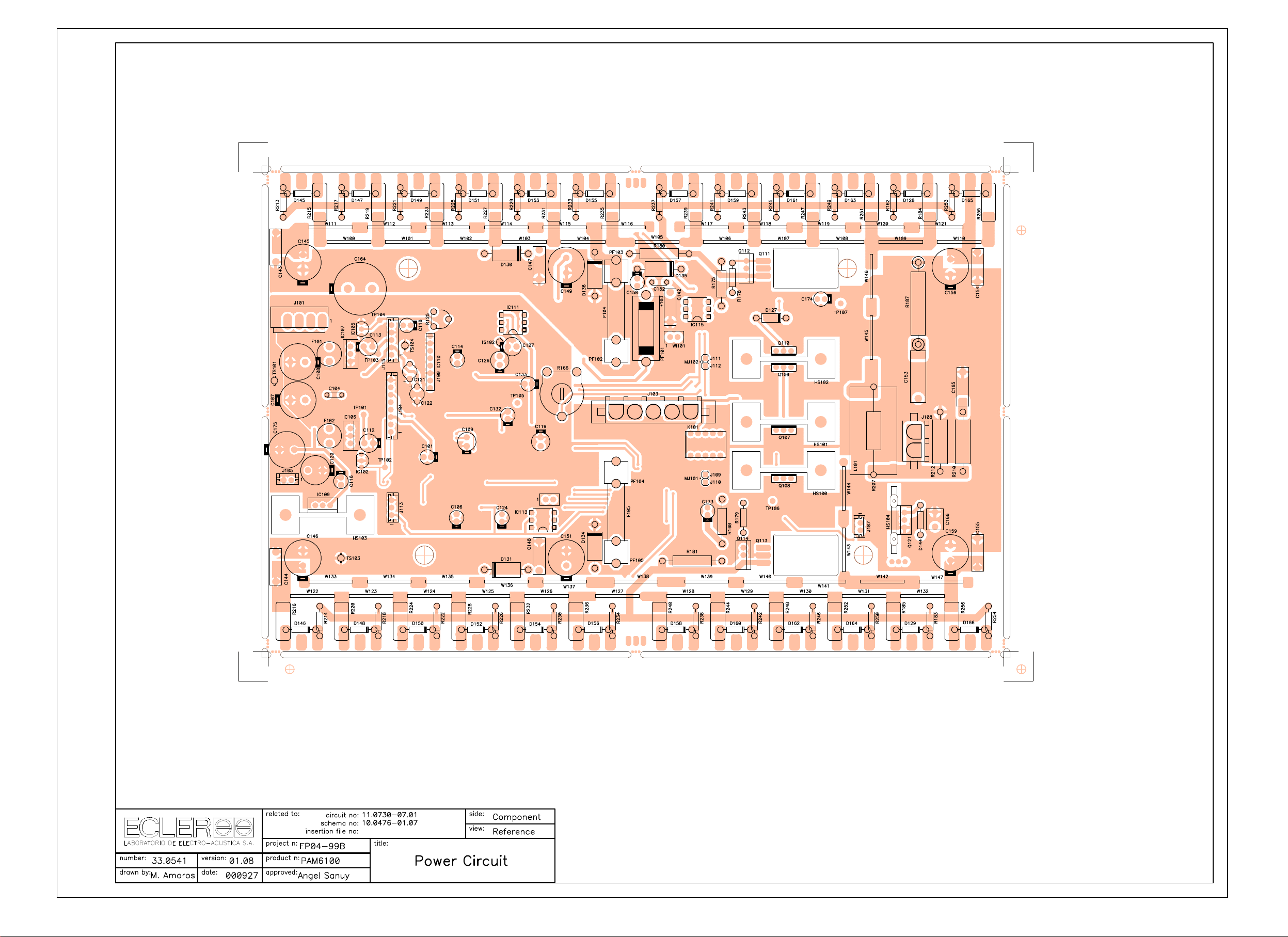
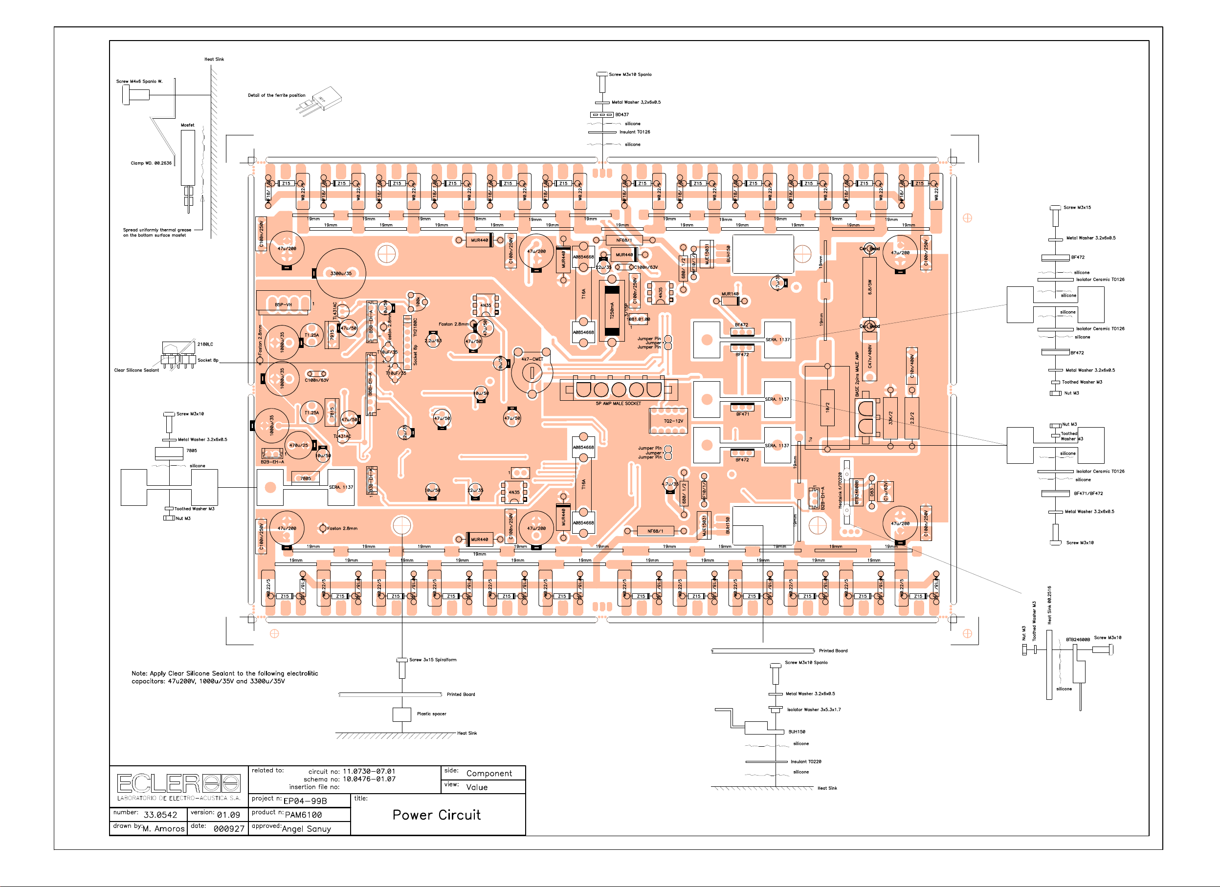
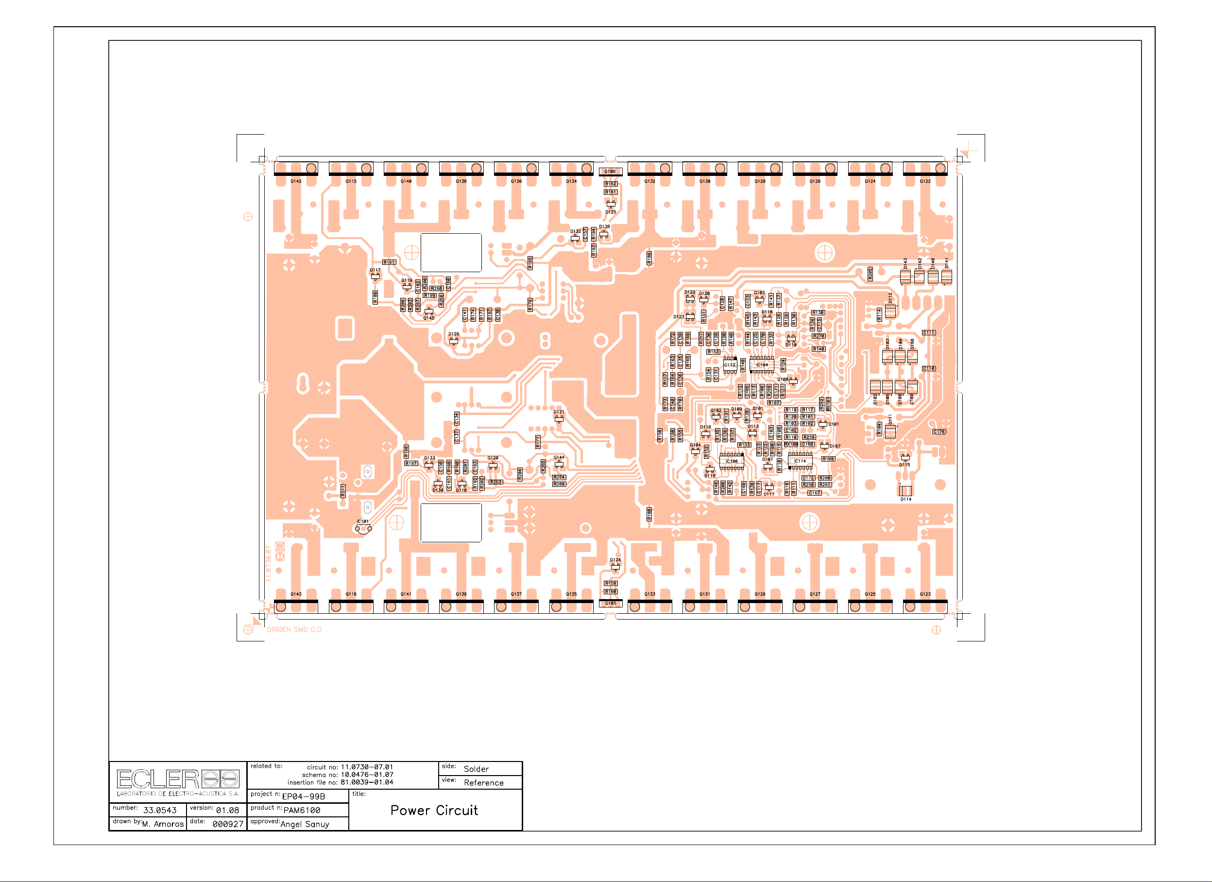
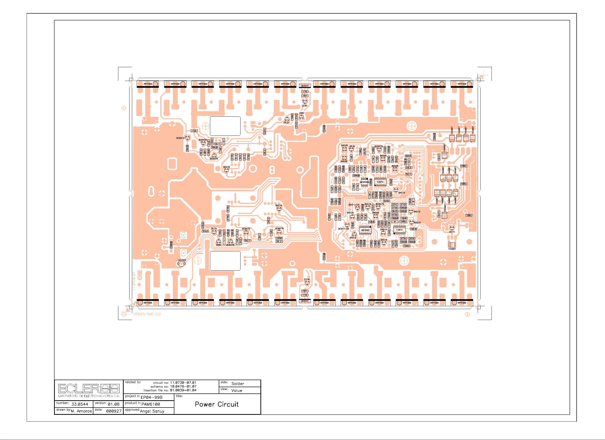
PARTS LIST: PRINTED CIRCUIT 11.0833.04.00
Q
Code
Description
Reference
1
FCCE250470
47u/50
C100
1
FCCE250470
47u/50
C101
1
FCCE250470
47u/50
C102
1
FCCE250470
47u/50
C103
1
FCXCN41000
100n
C104
1
FCXCN41000
100n
C105
1
FCXCN41000
100n
C106
1
FCXCN41000
100n
C107
1
FCXCN41000
100n
C108
1
FCXCN41000
100n
C109
1
FCXCN41000
100n
C110
1
FCXCN41000
100n
C111
1
FCXCN21000
100p
C112
1
FCXCN21000
100p
C113
1
FCXCN21000
100p
C114
1
FCXCN21000
100p
C115
1
FCXCN12201
22p 2%
C116
1
FCXCN12201
22p 2%
C117
1
FCXCN12201
22p 2%
C118
1
FCXCN12201
22p 2%
C119
1
FCCE250100
10u/50
C120
1
FCCE250100
10u/50
C121
1
FCXCN42200
220n
C122
1
FCXCN42200
220n
C123
1
FCXCN42200
220n
C124
1
FCXCN42200
220n
C125
1
FCXCN42200
220n
C126
1
FCXCN42200
220n
C127
1
FCCIPAM833
11.0833 Printed Board
CI100
1
FCXDDBAS28
BAS28
D100
1
FCXDDBAS28
BAS28
D101
1
FCXDDBAS28
BAS28
D102
1
FCXDDBAS28
BAS28
D103
1
FCXDDBAS16
BAS16
D104
1
FCXDDBAS16
BAS16
D105
1
FCIC553200
NE5532AP
IC100
1
FCIC553200
NE5532AP
IC101
1
FCIC072010
TL072
IC102
1
FCIC072010
TL072
IC103
1
FCIC071010
TL071
IC104
1
FCBASX0900
YKF52-5005
J100
1
FCBASX1000
YKF52-5003
J101
1
FCBASX0900
YKF52-5005
J102
1
FCBASX1000
YKF52-5003
J103
1
FCCTM00040
B4B-EH-A
J104
1
FCCTM00070
B7B-EH-A
J152
1
FCCHK00680
68uH
L100
1
FCCHK00680
68uH
L101
1
FCCHK00680
68uH
L102
1
FCCHK00680
68uH
L103
1
FCMJ000100
Jumper
MJ106
1
FCMJ000100
Jumper
MJ107
1
FCXR151000
100k0
R100
1
FCXR151000
100k0
R101
40-0065-0205 EP04-99B.xls 1 of 3
Page 19

PARTS LIST: PRINTED CIRCUIT 11.0833.04.00
Q
Code
Description
Reference
1
FCXR151000
100k0
R102
1
FCXR151000
100k0
R103
1
FCXR121000
100.0
R104
1
FCXR121000
100.0
R105
1
FCXR121000
100.0
R106
1
FCXR121000
100.0
R107
1
FCXR242430
24k3 0.5%
R108
1
FCXR242430
24k3 0.5%
R109
1
FCXR242430
24k3 0.5%
R110
1
FCXR242430
24k3 0.5%
R111
1
FCXR242430
24k3 0.5%
R112
1
FCXR242430
24k3 0.5%
R113
1
FCXR242430
24k3 0.5%
R114
1
FCXR242430
24k3 0.5%
R115
1
FCXR131000
1k0
R116
1
FCXR131000
1k0
R117
1
FCXR115620
56.2
R118
1
FCXR115620
56.2
R119
1
FCXR131000
1k0
R120
1
FCXR131000
1k0
R121
1
FCXR153400
340k
R122
1
FCXR153400
340k
R123
1
FCXR071000
10M
R124
1
FCXR071000
10M
R125
1
FCXR141820
18k2
R126
1
FCXR141130
11k3
R127
1
FCXR139090
9k09
R128
1
FCXR131500
1k50
R129
1
FCXR141820
18k2
R130
1
FCXR141130
11k3
R131
1
FCXR139090
9k09
R132
1
FCXR131500
1k50
R133
1
FCXR147500
75k0
R134
1
FCXR147500
75k0
R135
1
FCXR144750
47k5
R136
1
FCXR144750
47k5
R137
1
FCXR143650
36k5
R138
1
FCXR143650
36k5
R139
1
FCXR071000
10M
R140
1
FCXR071000
10M
R141
1
FCXR143650
36k5
R142
1
FCXR143650
36k5
R143
1
FCXR242430
24k3 0.5%
R144
1
FCXR242430
24k3 0.5%
R145
1
FCXR141820
18k2
R146
1
FCXR141820
18k2
R147
1
FCXR115620
56.2
R148
1
FCXR115620
56.2
R149
1
FCXR242430
24k3 0.5%
R150
1
FCXR242430
24k3 0.5%
R151
1
FCXR131500
1k50
R152
1
FCINTAP080
NS42J11
S100
1
FCINTD7500
SS050
S101
1
FC6K058460
1058.04.60
WI102
40-0065-0205 EP04-99B.xls 2 of 3
Page 20

PARTS LIST: PRINTED CIRCUIT 11.0833.04.00
Q
Code
Description
Reference
1
FC6K058460
1058.04.60
WI103
40-0065-0205 EP04-99B.xls 3 of 3
Page 21
Page 22
Page 23
Page 24
Page 25

PARTS LIST: PRINTED CIRCUIT 11.0730.07.01
Q
Code
Description
Reference
1
FCCE200220
22u/35
C101
1
FCXCN44700
470n
C102
1
FCXCN44700
470n
C103
1
FCCDK11000
C100n/63V
C104
1
FCXCN44700
470n
C105
1
FCCE250100
10u/50
C106
1
FCCE211000
1000u/35
C107
1
FCCE211000
1000u/35
C108
1
FCCE250470
47u/50
C109
1
FCXCN41000
100n
C110
1
FCXCN41000
100n
C111
1
FCCE250470
47u/50
C112
1
FCCE250470
47u/50
C113
1
FCCE300022
2.2u/63
C114
1
FCXCN40010
1n
C115
1
FCCE250100
10u/50
C116
1
FCXCN41000
100n
C117
1
FCCE250100
10u/50
C118
1
FCCE250470
47u/50
C119
1
FCCE154700
470u/25
C120
1
FCCG001000
T10uF/35
C121
1
FCCG001000
T10uF/35
C122
1
FCXCN41000
100n
C123
1
FCCE200220
22u/35
C124
1
FCXCN12200
22p
C125
1
FCCE250470
47u/50
C126
1
FCCE250470
47u/50
C127
1
FCXCN21000
100p
C128
1
FCXCN12200
22p
C129
1
FCXCN12200
22p
C130
1
FCXCN11500
15p
C131
1
FCCE250100
10u/50
C132
1
FCCE250100
10u/50
C133
1
FCXCN44700
470n
C134
1
FCXCN11200
12p
C135
1
FCXCN11200
12p
C136
1
FCXCN44700
470n
C137
1
FCXCN44700
470n
C138
1
FCXCN12200
22p
C139
1
FCXCN12200
22p
C140
1
FCXCN44700
470n
C141
1
FCCDN11000
C100n/250V
C142
1
FCCDN11000
C100n/250V
C143
1
FCCDN11000
C100n/250V
C144
1
FCCE350047
47u/200
C145
1
FCCE350047
47u/200
C146
1
FCCDN11000
C100n/250V
C147
1
FCCDN11000
C100n/250V
C148
1
FCCE350047
47u/200
C149
1
FCCE200220
22u/35
C150
1
FCCE350047
47u/200
C151
1
FCCDK11000
C100n/63V
C152
1
FCCDH71047
C47n/400V
C153
1
FCCDN11000
C100n/250V
C154
1
FCCDN11000
C100n/250V
C155
1
FCCE350047
47u/200
C156
40-0065-0206 EP04-99B.xls 1 of 11
Page 26

PARTS LIST: PRINTED CIRCUIT 11.0730.07.01
Q
Code
Description
Reference
1
FCXCN41000
100n
C157
1
FCXCN41000
100n
C158
1
FCCE350047
47u/200
C159
1
FCXCN40010
1n
C160
1
FCXCN40010
1n
C161
1
FCXCN40022
2n2
C162
1
FCXCN40022
2n2
C163
1
FCCE213300
3300u/35
C164
1
FCCDH71011
C10n/400V
C165
1
FCCDK20010
C1u/63V
C166
1
FCXCN41000
100n
C167
1
FCXCN41000
100n
C168
1
FCXCN41000
100n
C169
1
FCXCN41000
100n
C170
1
FCXCN41000
100n
C171
1
FCXCN44700
470n
C172
1
FCCE200047
4.7u/35
C173
1
FCCE200047
4.7u/35
C174
1
FCCE211000
1000u/35
C175
1
FCXCN41000
100n
C176
1
FCPERL2550
Cer. Bead
CB101
1
FCPERL2550
Cer. Bead
CB102
1
FCPERL2550
Cer. Bead
CB103
1
FCPERL2550
Cer. Bead
CB104
1
FCCIPAM730
11.0730 Printed Board
CI101
1
FCXDDBAS16
BAS16
D101
1
FCXDD40070
1N4007
D102
1
FCXDD40070
1N4007
D103
1
FCXDD40070
1N4007
D104
1
FCXDD40070
1N4007
D105
1
FCXDD40070
1N4007
D106
1
FCXDDBAS16
BAS16
D107
1
FCXDDBAS16
BAS16
D108
1
FCXDDBAS16
BAS16
D109
1
FCXDDBAS28
BAS28
D110
1
FCXDD40070
1N4007
D111
1
FCXDD40070
1N4007
D112
1
FCXDDBAS28
BAS28
D113
1
FCXDD40070
1N4007
D114
1
FCXZ000091
Z9.1V
D115
1
FCXDDBAS16
BAS16
D116
1
FCXDDBAS16
BAS16
D117
1
FCXDDBAS28
BAS28
D118
1
FCXDDBAS16
BAS16
D119
1
FCXZ000082
Z8.2V
D120
1
FCXDDBAS16
BAS16
D121
1
FCXDDBAS28
BAS28
D122
1
FCXDDBAS28
BAS28
D123
1
FCXZ000039
Z3.9V
D124
1
FCXZ000039
Z3.9V
D125
1
FCXDDBAS16
BAS16
D126
1
FCDDMUR140
MUR140
D127
1
FCDD041500
Z15
D128
1
FCDD041500
Z15
D129
1
FCDDMUR440
MUR440
D130
1
FCDDMUR440
MUR440
D131
40-0065-0206 EP04-99B.xls 2 of 11
Page 27

PARTS LIST: PRINTED CIRCUIT 11.0730.07.01
Q
Code
Description
Reference
1
FCXZ000082
Z8.2V
D132
1
FCXZ000082
Z8.2V
D133
1
FCDDMUR440
MUR440
D134
1
FCDDMUR440
MUR440
D135
1
FCDDMUR440
MUR440
D136
1
FCXZ000680
Z68V
D138
1
FCXZ000680
Z68V
D139
1
FCXDD40070
1N4007
D140
1
FCXDD40070
1N4007
D141
1
FCXDD40070
1N4007
D142
1
FCXDD40070
1N4007
D143
1
FCDIDB3000
DB3
D144
1
FCDD041500
Z15
D145
1
FCDD041500
Z15
D146
1
FCDD041500
Z15
D147
1
FCDD041500
Z15
D148
1
FCDD041500
Z15
D149
1
FCDD041500
Z15
D150
1
FCDD041500
Z15
D151
1
FCDD041500
Z15
D152
1
FCDD041500
Z15
D153
1
FCDD041500
Z15
D154
1
FCDD041500
Z15
D155
1
FCDD041500
Z15
D156
1
FCDD041500
Z15
D157
1
FCDD041500
Z15
D158
1
FCDD041500
Z15
D159
1
FCDD041500
Z15
D160
1
FCDD041500
Z15
D161
1
FCDD041500
Z15
D162
1
FCDD041500
Z15
D163
1
FCDD041500
Z15
D164
1
FCDD041500
Z15
D165
1
FCDD041500
Z15
D166
1
FCXDDBAS16
BAS16
D167
1
FCXDD40070
1N4007
D168
1
FCXDD40070
1N4007
D169
1
FCFUS40125
T1.25A
F101
1
FCFUS40125
T1.25A
F102
1
FCFUS50080
T250mA
F103
1
FCFUS60400
T16A
F104
1
FCFUS60400
T16A
F105
1
FCFER43220
Ferrite
FB101
1
FCFER43220
Ferrite
FB102
1
FCFER43220
Ferrite
FB103
1
FCFER43220
Ferrite
FB104
1
FCFER43220
Ferrite
FB105
1
FCFER43220
Ferrite
FB106
1
FCFER43220
Ferrite
FB107
1
FCFER43220
Ferrite
FB108
1
FCFER43220
Ferrite
FB109
1
FCFER43220
Ferrite
FB110
1
FCFER43220
Ferrite
FB111
1
FCFER43220
Ferrite
FB112
1
FCFER43220
Ferrite
FB113
1
FCFER43220
Ferrite
FB114
40-0065-0206 EP04-99B.xls 3 of 11
Page 28

PARTS LIST: PRINTED CIRCUIT 11.0730.07.01
Q
Code
Description
Reference
1
FCFER43220
Ferrite
FB115
1
FCFER43220
Ferrite
FB116
1
FCFER43220
Ferrite
FB117
1
FCFER43220
Ferrite
FB118
1
FCFER43220
Ferrite
FB119
1
FCFER43220
Ferrite
FB120
1
FCFER43220
Ferrite
FB121
1
FCFER43220
Ferrite
FB122
1
FCFER43220
Ferrite
FB123
1
FCFER43220
Ferrite
FB124
1
FCFER43220
Ferrite
FB125
1
FCFER43220
Ferrite
FB126
1
FCFER43220
Ferrite
FB127
1
FCFER43220
Ferrite
FB128
1
FCFER43220
Ferrite
FB129
1
FCFER43220
Ferrite
FB130
1
FCFER43220
Ferrite
FB131
1
FCFER43220
Ferrite
FB132
1
FCFER43220
Ferrite
FB133
1
FCFER43220
Ferrite
FB134
1
FCFER43220
Ferrite
FB135
1
FCFER43220
Ferrite
FB136
1
FCFER43220
Ferrite
FB137
1
FCFER43220
Ferrite
FB138
1
FCFER43220
Ferrite
FB139
1
FCFER43220
Ferrite
FB140
1
FCFER43220
Ferrite
FB141
1
FCFER43220
Ferrite
FB142
1
FCFER43220
Ferrite
FB143
1
FCFER43220
Ferrite
FB144
1
FCFER43220
Ferrite
FB145
1
FCFER43220
Ferrite
FB146
1
FCFER43220
Ferrite
FB147
1
FCFER43220
Ferrite
FB148
1
FCRAD12636
SERA. 1137
HS100
1
FCRAD12636
SERA. 1137
HS101
1
FCRAD12636
SERA. 1137
HS102
1
FCRAD12636
SERA. 1137
HS103
1
FCMECT0220
Heatsink f/TO220
HS104
1
FCRAD03000
Heatsink f/ Power Module
HS105
1
FCRAD03000
Heatsink f/ Power Module
HS106
1
FCIC350000
LM35DZ
IC101
1
FCIC431000
TL431AC
IC102
1
FCIC074010
TL074
IC104
1
FCIC431000
TL431AC
IC105
1
FCREG78150
7815
IC106
1
FCREG79150
7915
IC107
1
FCIC401060
40106B
IC108
1
FCREG78050
7805
IC109
1
FCIC218000
TH2180C
IC110
1
FCIC435000
4N35
IC111
1
FCIC553410
NE5534A
IC112
1
FCIC435000
4N35
IC113
1
FCIC074010
TL074
IC114
1
FCIC435000
4N35
IC115
1
FCMICTO126
Insulant TO126
IN100
40-0065-0206 EP04-99B.xls 4 of 11
Page 29

PARTS LIST: PRINTED CIRCUIT 11.0730.07.01
Q
Code
Description
Reference
1
FCMICTO126
Insulant TO126
IN101
1
FCMICTO220
Insulant TO220
IN102
1
FCMICTO220
Insulant TO220
IN103
1
FCTERM0080
Socket 8p
J100
1
FCCTJ10050
B5P-VH
J101
1
FCCTAMP050
5P AMP MALE SOCKET
J103
1
FCCTM00080
B8B-EH-A
J104
1
FCCTM00020
B2B-EH-A
J105
1
FCCTM00020
B2B-EH-A
J107
1
FCCTAMP020
BASE 2pins MALE AMP
J108
1
FCTERM0100
Jumper Pin
J109
1
FCTERM0100
Jumper Pin
J110
1
FCTERM0100
Jumper Pin
J111
1
FCTERM0100
Jumper Pin
J112
1
FCCTM00030
B3B-EH-A
J113
1
FCCTM00050
B5B-EH-A
J115
1
FCREL00300
TQ2-12V
K101
1
FCIND00100
1u
L101
1
FCMJ000100
Jumper
MJ101
1
FCMJ000100
Jumper
MJ102
1
FCPINZAM00
Clamp WD. 00.2636
MP100
1
FCPINZAM00
Clamp WD. 00.2636
MP101
1
FCPINZAM00
Clamp WD. 00.2636
MP102
1
FCPINZAM00
Clamp WD. 00.2636
MP103
1
FCTUE00300
Nut M3
NV100
1
FCTUE00300
Nut M3
NV101
1
FCTUE00300
Nut M3
NV102
1
FCTUE00300
Nut M3
NV103
1
FCTUE00300
Nut M3
NV104
1
FCPORF3150
3/15P
PF101
1
FCPORF0100
A0854668
PF102
1
FCPORF0100
A0854668
PF103
1
FCPORF0100
A0854668
PF104
1
FCPORF0100
A0854668
PF105
1
FCXTT08470
BC847B
Q101
1
FCXTT08170
BC817/25
Q102
1
FCXTT08570
BC857B
Q103
1
FCXTT08170
BC817/25
Q104
1
FCTR437000
BD437
Q105
1
FCTR437000
BD437
Q106
1
FCTR471000
BF471
Q107
1
FCTR472000
BF472
Q108
1
FCTR472000
BF472
Q109
1
FCTR472000
BF472
Q110
1
FCTR150000
BUH150
Q111
1
FCTR150310
MJE15031
Q112
1
FCTR150000
BUH150
Q113
1
FCTR150310
MJE15031
Q114
1
FCTR360000
IRFP360
Q115
1
FCTR360000
IRFP360
Q116
1
FCXTT08470
BC847B
Q117
1
FCXTT08470
BC847B
Q118
1
FCXTT08470
BC847B
Q119
1
FCXTT08470
BC847B
Q120
1
FCTI246000
BTB24600B
Q121
1
FCTR360000
IRFP360
Q122
40-0065-0206 EP04-99B.xls 5 of 11
Page 30

PARTS LIST: PRINTED CIRCUIT 11.0730.07.01
Q
Code
Description
Reference
1
FCTR360000
IRFP360
Q123
1
FCTR360000
IRFP360
Q124
1
FCTR360000
IRFP360
Q125
1
FCTR360000
IRFP360
Q126
1
FCTR360000
IRFP360
Q127
1
FCTR360000
IRFP360
Q128
1
FCTR360000
IRFP360
Q129
1
FCTR360000
IRFP360
Q130
1
FCTR360000
IRFP360
Q131
1
FCTR360000
IRFP360
Q132
1
FCTR360000
IRFP360
Q133
1
FCTR360000
IRFP360
Q134
1
FCTR360000
IRFP360
Q135
1
FCTR360000
IRFP360
Q136
1
FCTR360000
IRFP360
Q137
1
FCTR360000
IRFP360
Q138
1
FCTR360000
IRFP360
Q139
1
FCTR360000
IRFP360
Q140
1
FCTR360000
IRFP360
Q141
1
FCTR360000
IRFP360
Q142
1
FCTR360000
IRFP360
Q143
1
FCXTT08570
BC857B
Q144
1
FCXTT08570
BC857B
Q145
1
FCXR151000
100k0
R101
1
FCXR151000
100k0
R102
1
FCXR138250
8k25
R103
1
FCXR132210
2k21
R104
1
FCXR141000
10k0
R105
1
FCXR151000
100k0
R106
1
FCXR152260
226k
R107
1
FCXR141000
10k0
R108
1
FCXR121000
100.0
R109
1
FCXR151000
100k0
R110
1
FCXR132430
2k43
R111
1
FCXR061000
1M
R112
1
FCXR151000
100k0
R113
1
FCXR132210
2k21
R114
1
FCXR131000
1k0
R115
1
FCXR131270
1k27
R116
1
FCXR144750
47k5
R117
1
FCXR062200
2M2
R118
1
FCXR142210
22k1
R119
1
FCXR144750
47k5
R120
1
FCXR141000
10k0
R121
1
FCXR131820
1k82
R122
1
FCXR141000
10k0
R123
1
FCXR142000
20k0
R124
1
FCRJC61000
100k
R125
1
FCXR152260
226k
R126
1
FCXR151000
100k0
R127
1
FCXR142210
22k1
R128
1
FCXR062200
2M2
R129
1
FCXR148450
84k5
R130
1
FCXR151000
100k0
R131
1
FCXR142000
20k0
R132
1
FCXR141000
10k0
R133
40-0065-0206 EP04-99B.xls 6 of 11
Page 31

PARTS LIST: PRINTED CIRCUIT 11.0730.07.01
Q
Code
Description
Reference
1
FCXR121000
100.0
R134
1
FCXR152870
287k
R135
1
FCXR117500
75.0
R136
1
FCXR117500
75.0
R137
1
FCXR142000
20k0
R138
1
FCXR141000
10k0
R139
1
FCXR135110
5k11
R140
1
FCXR131820
1k82
R141
1
FCXR151000
100k0
R142
1
FCXR131000
1k0
R143
1
FCXR142000
20k0
R144
1
FCXR061000
1M
R145
1
FCXR131820
1k82
R146
1
FCXR134750
4k75
R147
1
FCXR131000
1k0
R148
1
FCXR151000
100k0
R149
1
FCXR131000
1k0
R150
1
FCXR131000
1k0
R151
1
FCXR141000
10k0
R152
1
FCXR151000
100k0
R153
1
FCXR071000
10M
R154
1
FCXR121780
178
R155
1
FCXR141000
10k0
R156
1
FCXR131000
1k0
R157
1
FCXR131000
1k0
R158
1
FCXR127870
787
R159
1
FCXR121780
178
R160
1
FCXR127870
787
R161
1
FCXR121780
178
R162
1
FCXR131500
1k50
R163
1
FCXR131500
1k50
R164
1
FCXR131210
1k21
R165
1
FCRJP44700
4k7-CMET
R166
1
FCXR113320
33.2
R167
1
FCRC236800
680/ 1/2
R168
1
FCXR151000
100k0
R169
1
FCXR151000
100k0
R170
1
FCXR128250
825
R171
1
FCXR141000
10k0
R172
1
FCXR141000
10k0
R173
1
FCXR113320
33.2
R174
1
FCRC236800
680/ 1/2
R175
1
FCXR115620
56.2
R176
1
FCXR115620
56.2
R177
1
FCRF221000
NF10/1/2
R178
1
FCRF221000
NF10/1/2
R179
1
FCRF426800
NF68/1
R180
1
FCRF426800
NF68/1
R181
1
FCRF221800
NF18/ 1/2
R182
1
FCRF221800
NF18/ 1/2
R183
1
FCRY000100
W0.22/5
R184
1
FCRY000100
W0.22/5
R185
1
FCXR151500
150k0
R186
1
FCRY000250
6.8/5W
R187
1
FCXR151500
150k0
R188
1
FCXR121000
100.0
R189
40-0065-0206 EP04-99B.xls 7 of 11
Page 32

PARTS LIST: PRINTED CIRCUIT 11.0730.07.01
Q
Code
Description
Reference
1
FCXR121000
100.0
R190
1
FCXR131000
1k0
R191
1
FCXR131000
1k0
R192
1
FCXR143320
33k2
R193
1
FCXR143320
33k2
R194
1
FCXR142210
22k1
R195
1
FCXR143320
33k2
R196
1
FCXR143320
33k2
R197
1
FCXR142210
22k1
R198
1
FCXR121000
100.0
R199
1
FCXR125620
562
R200
1
FCXR121000
100.0
R201
1
FCXR125620
562
R202
1
FCXR123010
301
R203
1
FCXR123010
301
R204
1
FCXR151000
100k0
R205
1
FCXR115620
56.2
R206
1
FCRC521000
10/2
R207
1
FCXR151500
150k0
R208
1
FCXR115620
56.2
R209
1
FCRC512200
2.2/2
R210
1
FCXR151000
100k0
R211
1
FCRC553300
33K/2
R212
1
FCRF221800
NF18/ 1/2
R213
1
FCRF221800
NF18/ 1/2
R214
1
FCRY000100
W0.22/5
R215
1
FCRY000100
W0.22/5
R216
1
FCRF221800
NF18/ 1/2
R217
1
FCRF221800
NF18/ 1/2
R218
1
FCRY000100
W0.22/5
R219
1
FCRY000100
W0.22/5
R220
1
FCRF221800
NF18/ 1/2
R221
1
FCRF221800
NF18/ 1/2
R222
1
FCRY000100
W0.22/5
R223
1
FCRY000100
W0.22/5
R224
1
FCRF221800
NF18/ 1/2
R225
1
FCRF221800
NF18/ 1/2
R226
1
FCRY000100
W0.22/5
R227
1
FCRY000100
W0.22/5
R228
1
FCRF221800
NF18/ 1/2
R229
1
FCRF221800
NF18/ 1/2
R230
1
FCRY000100
W0.22/5
R231
1
FCRY000100
W0.22/5
R232
1
FCRF221800
NF18/ 1/2
R233
1
FCRF221800
NF18/ 1/2
R234
1
FCRY000100
W0.22/5
R235
1
FCRY000100
W0.22/5
R236
1
FCRF221800
NF18/ 1/2
R237
1
FCRF221800
NF18/ 1/2
R238
1
FCRY000100
W0.22/5
R239
1
FCRY000100
W0.22/5
R240
1
FCRF221800
NF18/ 1/2
R241
1
FCRF221800
NF18/ 1/2
R242
1
FCRY000100
W0.22/5
R243
1
FCRY000100
W0.22/5
R244
1
FCRF221800
NF18/ 1/2
R245
40-0065-0206 EP04-99B.xls 8 of 11
Page 33

PARTS LIST: PRINTED CIRCUIT 11.0730.07.01
Q
Code
Description
Reference
1
FCRF221800
NF18/ 1/2
R246
1
FCRY000100
W0.22/5
R247
1
FCRY000100
W0.22/5
R248
1
FCRF221800
NF18/ 1/2
R249
1
FCRF221800
NF18/ 1/2
R250
1
FCRY000100
W0.22/5
R251
1
FCRY000100
W0.22/5
R252
1
FCRF221800
NF18/ 1/2
R253
1
FCRF221800
NF18/ 1/2
R254
1
FCRY000100
W0.22/5
R255
1
FCRY000100
W0.22/5
R256
1
FCXR126040
604
R257
1
FCXR151000
100k0
R258
1
FCXR141000
10k0
R259
1
FCXR152050
205k
R260
1
FCXR151000
100k0
R261
1
FCXR141000
10k0
R262
1
FCXR135110
5k11
R263
1
FCXR141000
10k0
R264
1
FCXR131000
1k0
R265
1
FCXR131000
1k0
R266
1
FCXR141000
10k0
R267
1
FCXR135110
5k11
R268
1
FCXR149090
90k9
R269
1
FCXR115620
56.2
R270
1
FCXR000000
0
RX100
1
FCXR000000
0
RX101
1
FCT8040060
Screw M4x6 SPAN
SC100
1
FCT8040060
Screw M4x6 SPAN
SC101
1
FCT8040060
Screw M4x6 SPAN
SC102
1
FCT8040060
Screw M4x6 SPAN
SC103
1
FCT8040060
Screw M4x6 SPAN
SC104
1
FCT8040060
Screw M4x6 SPAN
SC105
1
FCT8040060
Screw M4x6 SPAN
SC106
1
FCT8040060
Screw M4x6 SPAN
SC107
1
FCT8040060
Screw M4x6 SPAN
SC108
1
FCT8040060
Screw M4x6 SPAN
SC109
1
FCT8040060
Screw M4x6 SPAN
SC110
1
FCT8040060
Screw M4x6 SPAN
SC111
1
FCT8030100
Screw M3x10 SPA
SC112
1
FCT8030100
Screw M3x10 SPA
SC113
1
FCT8030150
Screw 3x15 SPIRALFORM
SC114
1
FCT8030150
Screw 3x15 SPIRALFORM
SC115
1
FCT8030100
Screw M3x10 SPA
SC116
1
FCT8030100
Screw M3x10 SPA
SC117
1
FCT7503010
Screw M3x10
SC118
1
FCT7503010
Screw M3x10
SC119
1
FCT7503010
Screw M3x10
SC120
1
FCT7503010
Screw M3x10
SC121
1
FCT8030150
Screw M3x15
SC122
1
FCSEPPM000
Plastic Spacer f/board ct.
SC123
1
FCT8030150
Screw 3x15 SPIRALFORM
SC124
1
FCT8030150
Screw 3x15 SPIRALFORM
SC125
1
FCSEPPM000
Plastic Spacer f/board ct.
SC126
1
FCSEPPM000
Plastic Spacer f/board ct.
SC127
1
FCSEPPM000
Plastic Spacer f/board ct.
SC128
40-0065-0206 EP04-99B.xls 9 of 11
Page 34

PARTS LIST: PRINTED CIRCUIT 11.0730.07.01
Q
Code
Description
Reference
1
FCTERMF280
Faston 2.8mm
TS101
1
FCTERMF280
Faston 2.8mm
TS102
1
FCTERMF280
Faston 2.8mm
TS103
1
FCTERMF280
Faston 2.8mm
TS104
1
FCMECPON19
19mm
W100
1
FCMECPON19
19mm
W101
1
FCMECPON19
19mm
W102
1
FCMECPON19
19mm
W103
1
FCMECPON19
19mm
W104
1
FCMECPON19
19mm
W105
1
FCMECPON19
19mm
W106
1
FCMECPON19
19mm
W107
1
FCMECPON19
19mm
W108
1
FCMECPON19
19mm
W109
1
FCMECPON19
19mm
W110
1
FCMECPON19
19mm
W111
1
FCMECPON19
19mm
W112
1
FCMECPON19
19mm
W113
1
FCMECPON19
19mm
W114
1
FCMECPON19
19mm
W115
1
FCMECPON19
19mm
W116
1
FCMECPON19
19mm
W117
1
FCMECPON19
19mm
W118
1
FCMECPON19
19mm
W119
1
FCMECPON19
19mm
W120
1
FCMECPON19
19mm
W121
1
FCMECPON19
19mm
W122
1
FCMECPON19
19mm
W123
1
FCMECPON19
19mm
W124
1
FCMECPON19
19mm
W125
1
FCMECPON19
19mm
W126
1
FCMECPON19
19mm
W127
1
FCMECPON19
19mm
W128
1
FCMECPON19
19mm
W129
1
FCMECPON19
19mm
W130
1
FCMECPON19
19mm
W131
1
FCMECPON19
19mm
W132
1
FCMECPON19
19mm
W133
1
FCMECPON19
19mm
W134
1
FCMECPON19
19mm
W135
1
FCMECPON19
19mm
W136
1
FCMECPON19
19mm
W137
1
FCMECPON19
19mm
W138
1
FCMECPON19
19mm
W139
1
FCMECPON19
19mm
W140
1
FCMECPON19
19mm
W141
1
FCMECPON19
19mm
W142
1
FCMECPON19
19mm
W143
1
FCMECPON19
19mm
W144
1
FCMECPON19
19mm
W145
1
FCMECPON19
19mm
W146
1
FCMECPON19
19mm
W147
1
FCARM32000
Metal Washer 3.2x6x0.5
WA100
1
FCARM32000
Metal Washer 3.2x6x0.5
WA101
1
FCARM32000
Metal Washer 3.2x6x0.5
WA102
1
FCARM32000
Metal Washer 3.2x6x0.5
WA103
40-0065-0206 EP04-99B.xls 10 of 11
Page 35

PARTS LIST: PRINTED CIRCUIT 11.0730.07.01
Q
Code
Description
Reference
1
FCARM32000
Metal Washer 3.2x6x0.5
WA104
1
FCARDE0300
Toothed Washer f/M3
WA105
1
FCARM32000
Metal Washer 3.2x6x0.5
WA106
1
FCARDE0300
Toothed Washer f/M3
WA107
1
FCARDE0300
Toothed Washer f/M3
WA108
1
FCARDE0300
Toothed Washer f/M3
WA109
1
FCARDE0300
Toothed Washer f/M3
WA110
1
FCARM32000
Metal Washer 3.2x6x0.5
WA114
1
FCARAT0000
Washer Ins. Tr. 3x5.3x1.7
WA115
1
FCSEPCE126
Ceramic Isolator TO126
WA116
1
FCSEPCE126
Ceramic Isolator TO126
WA117
1
FCSEPCE126
Ceramic Isolator TO126
WA118
1
FCSEPCE126
Ceramic Isolator TO126
WA119
1
FCARM32000
Metal Washer 3.2x6x0.5
WA120
1
FCARAT0000
Washer Ins. Tr. 3x5.3x1.7
WA122
1
FC4G081100
1081.01.00
WI101
40-0065-0206 EP04-99B.xls 11 of 11
Page 36

Page 37

Page 38

Page 39

Page 40

PARTS LIST: PRINTED CIRCUIT 11.0730.07.00
Q
Code
Description
Reference
1
FCCE200220
22u/35
C101
1
FCXCN44700
470n
C102
1
FCXCN44700
470n
C103
1
FCCDK11000
C100n/63V
C104
1
FCXCN44700
470n
C105
1
FCCE250100
10u/50
C106
1
FCCE211000
1000u/35
C107
1
FCCE211000
1000u/35
C108
1
FCCE250470
47u/50
C109
1
FCXCN41000
100n
C110
1
FCXCN41000
100n
C111
1
FCCE250470
47u/50
C112
1
FCCE250470
47u/50
C113
1
FCCE300022
2.2u/63
C114
1
FCXCN40010
1n
C115
1
FCCE250100
10u/50
C116
1
FCXCN41000
100n
C117
1
FCCE250100
10u/50
C118
1
FCCE250470
47u/50
C119
1
FCCE154700
470u/25
C120
1
FCCG001000
T10uF/35
C121
1
FCCG001000
T10uF/35
C122
1
FCXCN41000
100n
C123
1
FCCE200220
22u/35
C124
1
FCXCN12200
22p
C125
1
FCCE250470
47u/50
C126
1
FCCE250470
47u/50
C127
1
FCXCN21000
100p
C128
1
FCXCN12200
22p
C129
1
FCXCN12200
22p
C130
1
FCXCN11500
15p
C131
1
FCCE250100
10u/50
C132
1
FCCE250100
10u/50
C133
1
FCXCN44700
470n
C134
1
FCXCN11200
12p
C135
1
FCXCN11200
12p
C136
1
FCXCN44700
470n
C137
1
FCXCN44700
470n
C138
1
FCXCN12200
22p
C139
1
FCXCN12200
22p
C140
1
FCXCN44700
470n
C141
1
FCCDN11000
C100n/250V
C142
1
FCCDN11000
C100n/250V
C143
1
FCCDN11000
C100n/250V
C144
1
FCCE350047
47u/200
C145
1
FCCE350047
47u/200
C146
1
FCCDN11000
C100n/250V
C147
1
FCCDN11000
C100n/250V
C148
1
FCCE350047
47u/200
C149
1
FCCE200220
22u/35
C150
1
FCCE350047
47u/200
C151
1
FCCDK11000
C100n/63V
C152
1
FCCDH71047
C47n/400V
C153
1
FCCDN11000
C100n/250V
C154
40-0065-0205 EP04-99B.xls 1 of 11
Page 41

PARTS LIST: PRINTED CIRCUIT 11.0730.07.00
Q
Code
Description
Reference
1
FCCDN11000
C100n/250V
C155
1
FCCE350047
47u/200
C156
1
FCXCN41000
100n
C157
1
FCXCN41000
100n
C158
1
FCCE350047
47u/200
C159
1
FCXCN40010
1n
C160
1
FCXCN40010
1n
C161
1
FCXCN40022
2n2
C162
1
FCXCN40022
2n2
C163
1
FCCE213300
3300u/35
C164
1
FCCDH71011
C10n/400V
C165
1
FCCDK20010
C1u/63V
C166
1
FCXCN41000
100n
C167
1
FCXCN41000
100n
C168
1
FCXCN41000
100n
C169
1
FCXCN41000
100n
C170
1
FCXCN41000
100n
C171
1
FCXCN44700
470n
C172
1
FCCE200047
4.7u/35
C173
1
FCCE200047
4.7u/35
C174
1
FCCE211000
1000u/35
C175
1
FCXCN41000
100n
C176
1
FCPERL2550
Cer. Bead
CB101
1
FCPERL2550
Cer. Bead
CB102
1
FCPERL2550
Cer. Bead
CB103
1
FCPERL2550
Cer. Bead
CB104
1
FCCIPAM730
11.0730 Printed Board
CI101
1
FCXDDBAS16
BAS16
D101
1
FCXDD40070
1N4007
D102
1
FCXDD40070
1N4007
D103
1
FCXDD40070
1N4007
D104
1
FCXDD40070
1N4007
D105
1
FCXDD40070
1N4007
D106
1
FCXDDBAS16
BAS16
D107
1
FCXDDBAS16
BAS16
D108
1
FCXDDBAS16
BAS16
D109
1
FCXDDBAS28
BAS28
D110
1
FCXDD40070
1N4007
D111
1
FCXDD40070
1N4007
D112
1
FCXDDBAS28
BAS28
D113
1
FCXDD40070
1N4007
D114
1
FCXZ000091
Z9.1V
D115
1
FCXDDBAS16
BAS16
D116
1
FCXDDBAS16
BAS16
D117
1
FCXDDBAS28
BAS28
D118
1
FCXDDBAS16
BAS16
D119
1
FCXZ000082
Z8.2V
D120
1
FCXDDBAS16
BAS16
D121
1
FCXDDBAS28
BAS28
D122
1
FCXDDBAS28
BAS28
D123
1
FCXZ000039
Z3.9V
D124
1
FCXZ000039
Z3.9V
D125
1
FCXDDBAS16
BAS16
D126
1
FCDDMUR140
MUR140
D127
40-0065-0205 EP04-99B.xls 2 of 11
Page 42

PARTS LIST: PRINTED CIRCUIT 11.0730.07.00
Q
Code
Description
Reference
1
FCDD041500
Z15
D128
1
FCDD041500
Z15
D129
1
FCDDMUR440
MUR440
D130
1
FCDDMUR440
MUR440
D131
1
FCXZ000082
Z8.2V
D132
1
FCXZ000082
Z8.2V
D133
1
FCDDMUR440
MUR440
D134
1
FCDDMUR440
MUR440
D135
1
FCDDMUR440
MUR440
D136
1
FCXZ000680
Z68V
D138
1
FCXZ000680
Z68V
D139
1
FCXDD40070
1N4007
D140
1
FCXDD40070
1N4007
D141
1
FCXDD40070
1N4007
D142
1
FCXDD40070
1N4007
D143
1
FCDIDB3000
DB3
D144
1
FCDD041500
Z15
D145
1
FCDD041500
Z15
D146
1
FCDD041500
Z15
D147
1
FCDD041500
Z15
D148
1
FCDD041500
Z15
D149
1
FCDD041500
Z15
D150
1
FCDD041500
Z15
D151
1
FCDD041500
Z15
D152
1
FCDD041500
Z15
D153
1
FCDD041500
Z15
D154
1
FCDD041500
Z15
D155
1
FCDD041500
Z15
D156
1
FCDD041500
Z15
D157
1
FCDD041500
Z15
D158
1
FCDD041500
Z15
D159
1
FCDD041500
Z15
D160
1
FCDD041500
Z15
D161
1
FCDD041500
Z15
D162
1
FCDD041500
Z15
D163
1
FCDD041500
Z15
D164
1
FCDD041500
Z15
D165
1
FCDD041500
Z15
D166
1
FCXDDBAS16
BAS16
D167
1
FCXDD40070
1N4007
D168
1
FCXDD40070
1N4007
D169
1
FCFUS40125
T1.25A
F101
1
FCFUS40125
T1.25A
F102
1
FCFUS50080
T250mA
F103
1
FCFUS60400
T16A
F104
1
FCFUS60400
T16A
F105
1
FCFER43220
Ferrite
FB101
1
FCFER43220
Ferrite
FB102
1
FCFER43220
Ferrite
FB103
1
FCFER43220
Ferrite
FB104
1
FCFER43220
Ferrite
FB105
1
FCFER43220
Ferrite
FB106
1
FCFER43220
Ferrite
FB107
1
FCFER43220
Ferrite
FB108
40-0065-0205 EP04-99B.xls 3 of 11
Page 43

PARTS LIST: PRINTED CIRCUIT 11.0730.07.00
Q
Code
Description
Reference
1
FCFER43220
Ferrite
FB109
1
FCFER43220
Ferrite
FB110
1
FCFER43220
Ferrite
FB111
1
FCFER43220
Ferrite
FB112
1
FCFER43220
Ferrite
FB113
1
FCFER43220
Ferrite
FB114
1
FCFER43220
Ferrite
FB115
1
FCFER43220
Ferrite
FB116
1
FCFER43220
Ferrite
FB117
1
FCFER43220
Ferrite
FB118
1
FCFER43220
Ferrite
FB119
1
FCFER43220
Ferrite
FB120
1
FCFER43220
Ferrite
FB121
1
FCFER43220
Ferrite
FB122
1
FCFER43220
Ferrite
FB123
1
FCFER43220
Ferrite
FB124
1
FCFER43220
Ferrite
FB125
1
FCFER43220
Ferrite
FB126
1
FCFER43220
Ferrite
FB127
1
FCFER43220
Ferrite
FB128
1
FCFER43220
Ferrite
FB129
1
FCFER43220
Ferrite
FB130
1
FCFER43220
Ferrite
FB131
1
FCFER43220
Ferrite
FB132
1
FCFER43220
Ferrite
FB133
1
FCFER43220
Ferrite
FB134
1
FCFER43220
Ferrite
FB135
1
FCFER43220
Ferrite
FB136
1
FCFER43220
Ferrite
FB137
1
FCFER43220
Ferrite
FB138
1
FCFER43220
Ferrite
FB139
1
FCFER43220
Ferrite
FB140
1
FCFER43220
Ferrite
FB141
1
FCFER43220
Ferrite
FB142
1
FCFER43220
Ferrite
FB143
1
FCFER43220
Ferrite
FB144
1
FCFER43220
Ferrite
FB145
1
FCFER43220
Ferrite
FB146
1
FCFER43220
Ferrite
FB147
1
FCFER43220
Ferrite
FB148
1
FCRAD12636
SERA. 1137
HS100
1
FCRAD12636
SERA. 1137
HS101
1
FCRAD12636
SERA. 1137
HS102
1
FCRAD12636
SERA. 1137
HS103
1
FCMECT0220
Heatsink f/TO220
HS104
1
FCRAD03000
Heatsink f/ Power Module
HS105
1
FCRAD03000
Heatsink f/ Power Module
HS106
1
FCIC350000
LM35DZ
IC101
1
FCIC431000
TL431AC
IC102
1
FCIC074010
TL074
IC104
1
FCIC431000
TL431AC
IC105
1
FCREG78150
7815
IC106
1
FCREG79150
7915
IC107
1
FCIC401060
40106B
IC108
40-0065-0205 EP04-99B.xls 4 of 11
Page 44

PARTS LIST: PRINTED CIRCUIT 11.0730.07.00
Q
Code
Description
Reference
1
FCREG78050
7805
IC109
1
FCIC218000
TH2180C
IC110
1
FCIC435000
4N35
IC111
1
FCIC553410
NE5534A
IC112
1
FCIC435000
4N35
IC113
1
FCIC074010
TL074
IC114
1
FCIC435000
4N35
IC115
1
FCMICTO126
Insulant TO126
IN100
1
FCMICTO126
Insulant TO126
IN101
1
FCMICTO220
Insulant TO220
IN102
1
FCMICTO220
Insulant TO220
IN103
1
FCTERM0080
Socket 8p
J100
1
FCCTJ10050
B5P-VH
J101
1
FCCTAMP050
5P AMP MALE SOCKET
J103
1
FCCTM00080
B8B-EH-A
J104
1
FCCTM00020
B2B-EH-A
J105
1
FCCTM00020
B2B-EH-A
J107
1
FCCTAMP020
BASE 2pins MALE AMP
J108
1
FCTERM0100
Jumper Pin
J109
1
FCTERM0100
Jumper Pin
J110
1
FCTERM0100
Jumper Pin
J111
1
FCTERM0100
Jumper Pin
J112
1
FCCTM00030
B3B-EH-A
J113
1
FCCTM00050
B5B-EH-A
J115
1
FCREL00300
TQ2-12V
K101
1
FCIND00100
1u
L101
1
FCMJ000100
Jumper
MJ101
1
FCMJ000100
Jumper
MJ102
1
FCPINZAM00
Clamp WD. 00.2636
MP100
1
FCPINZAM00
Clamp WD. 00.2636
MP101
1
FCPINZAM00
Clamp WD. 00.2636
MP102
1
FCPINZAM00
Clamp WD. 00.2636
MP103
1
FCTUE00300
Nut M3
NV100
1
FCTUE00300
Nut M3
NV101
1
FCTUE00300
Nut M3
NV102
1
FCTUE00300
Nut M3
NV103
1
FCTUE00300
Nut M3
NV104
1
FCPORF3150
3/15P
PF101
1
FCPORF0100
A0854668
PF102
1
FCPORF0100
A0854668
PF103
1
FCPORF0100
A0854668
PF104
1
FCPORF0100
A0854668
PF105
1
FCXTT08470
BC847B
Q101
1
FCXTT08170
BC817/25
Q102
1
FCXTT08570
BC857B
Q103
1
FCXTT08170
BC817/25
Q104
1
FCTR437000
BD437
Q105
1
FCTR437000
BD437
Q106
1
FCTR587000
BF587
Q107
1
FCTR588000
BF588
Q108
1
FCTR588000
BF588
Q109
1
FCTR588000
BF588
Q110
1
FCTR150000
BUH150
Q111
1
FCTR150310
MJE15031
Q112
40-0065-0205 EP04-99B.xls 5 of 11
Page 45

PARTS LIST: PRINTED CIRCUIT 11.0730.07.00
Q
Code
Description
Reference
1
FCTR150000
BUH150
Q113
1
FCTR150310
MJE15031
Q114
1
FCTR360000
IRFP360
Q115
1
FCTR360000
IRFP360
Q116
1
FCXTT08470
BC847B
Q117
1
FCXTT08470
BC847B
Q118
1
FCXTT08470
BC847B
Q119
1
FCXTT08470
BC847B
Q120
1
FCTI246000
BTB24600B
Q121
1
FCTR360000
IRFP360
Q122
1
FCTR360000
IRFP360
Q123
1
FCTR360000
IRFP360
Q124
1
FCTR360000
IRFP360
Q125
1
FCTR360000
IRFP360
Q126
1
FCTR360000
IRFP360
Q127
1
FCTR360000
IRFP360
Q128
1
FCTR360000
IRFP360
Q129
1
FCTR360000
IRFP360
Q130
1
FCTR360000
IRFP360
Q131
1
FCTR360000
IRFP360
Q132
1
FCTR360000
IRFP360
Q133
1
FCTR360000
IRFP360
Q134
1
FCTR360000
IRFP360
Q135
1
FCTR360000
IRFP360
Q136
1
FCTR360000
IRFP360
Q137
1
FCTR360000
IRFP360
Q138
1
FCTR360000
IRFP360
Q139
1
FCTR360000
IRFP360
Q140
1
FCTR360000
IRFP360
Q141
1
FCTR360000
IRFP360
Q142
1
FCTR360000
IRFP360
Q143
1
FCXTT08570
BC857B
Q144
1
FCXTT08570
BC857B
Q145
1
FCXR151000
100k0
R101
1
FCXR151000
100k0
R102
1
FCXR138250
8k25
R103
1
FCXR132210
2k21
R104
1
FCXR141000
10k0
R105
1
FCXR151000
100k0
R106
1
FCXR152260
226k
R107
1
FCXR141000
10k0
R108
1
FCXR121000
100.0
R109
1
FCXR151000
100k0
R110
1
FCXR132430
2k43
R111
1
FCXR061000
1M
R112
1
FCXR151000
100k0
R113
1
FCXR132210
2k21
R114
1
FCXR131000
1k0
R115
1
FCXR131270
1k27
R116
1
FCXR144750
47k5
R117
1
FCXR062200
2M2
R118
1
FCXR142210
22k1
R119
1
FCXR144750
47k5
R120
1
FCXR141000
10k0
R121
40-0065-0205 EP04-99B.xls 6 of 11
Page 46

PARTS LIST: PRINTED CIRCUIT 11.0730.07.00
Q
Code
Description
Reference
1
FCXR131820
1k82
R122
1
FCXR141000
10k0
R123
1
FCXR142000
20k0
R124
1
FCRJC61000
100k
R125
1
FCXR152260
226k
R126
1
FCXR151000
100k0
R127
1
FCXR142210
22k1
R128
1
FCXR062200
2M2
R129
1
FCXR148450
84k5
R130
1
FCXR151000
100k0
R131
1
FCXR142000
20k0
R132
1
FCXR141000
10k0
R133
1
FCXR121000
100.0
R134
1
FCXR152870
287k
R135
1
FCXR117500
75.0
R136
1
FCXR117500
75.0
R137
1
FCXR142000
20k0
R138
1
FCXR141000
10k0
R139
1
FCXR135110
5k11
R140
1
FCXR131820
1k82
R141
1
FCXR151000
100k0
R142
1
FCXR131000
1k0
R143
1
FCXR142000
20k0
R144
1
FCXR061000
1M
R145
1
FCXR131820
1k82
R146
1
FCXR134750
4k75
R147
1
FCXR131000
1k0
R148
1
FCXR151000
100k0
R149
1
FCXR131000
1k0
R150
1
FCXR131000
1k0
R151
1
FCXR141000
10k0
R152
1
FCXR151000
100k0
R153
1
FCXR071000
10M
R154
1
FCXR121780
178
R155
1
FCXR141000
10k0
R156
1
FCXR131000
1k0
R157
1
FCXR131000
1k0
R158
1
FCXR127870
787
R159
1
FCXR121780
178
R160
1
FCXR127870
787
R161
1
FCXR121780
178
R162
1
FCXR131500
1k50
R163
1
FCXR131500
1k50
R164
1
FCXR131210
1k21
R165
1
FCRJP44700
4k7-CMET
R166
1
FCXR113320
33.2
R167
1
FCRC236800
680/ 1/2
R168
1
FCXR151000
100k0
R169
1
FCXR151000
100k0
R170
1
FCXR128250
825
R171
1
FCXR141000
10k0
R172
1
FCXR141000
10k0
R173
1
FCXR113320
33.2
R174
1
FCRC236800
680/ 1/2
R175
40-0065-0205 EP04-99B.xls 7 of 11
Page 47

PARTS LIST: PRINTED CIRCUIT 11.0730.07.00
Q
Code
Description
Reference
1
FCXR115620
56.2
R176
1
FCXR115620
56.2
R177
1
FCRF221000
NF10/1/2
R178
1
FCRF221000
NF10/1/2
R179
1
FCRF426800
NF68/1
R180
1
FCRF426800
NF68/1
R181
1
FCRF221800
NF18/ 1/2
R182
1
FCRF221800
NF18/ 1/2
R183
1
FCRY000100
W0.22/5
R184
1
FCRY000100
W0.22/5
R185
1
FCXR151500
150k0
R186
1
FCRY000250
6.8/5W
R187
1
FCXR151500
150k0
R188
1
FCXR121000
100.0
R189
1
FCXR121000
100.0
R190
1
FCXR131000
1k0
R191
1
FCXR131000
1k0
R192
1
FCXR143320
33k2
R193
1
FCXR143320
33k2
R194
1
FCXR142210
22k1
R195
1
FCXR143320
33k2
R196
1
FCXR143320
33k2
R197
1
FCXR142210
22k1
R198
1
FCXR121000
100.0
R199
1
FCXR125620
562
R200
1
FCXR121000
100.0
R201
1
FCXR125620
562
R202
1
FCXR123010
301
R203
1
FCXR123010
301
R204
1
FCXR151000
100k0
R205
1
FCXR115620
56.2
R206
1
FCRC521000
10/2
R207
1
FCXR151500
150k0
R208
1
FCXR115620
56.2
R209
1
FCRC512200
2.2/2
R210
1
FCXR151000
100k0
R211
1
FCRC553300
33K/2
R212
1
FCRF221800
NF18/ 1/2
R213
1
FCRF221800
NF18/ 1/2
R214
1
FCRY000100
W0.22/5
R215
1
FCRY000100
W0.22/5
R216
1
FCRF221800
NF18/ 1/2
R217
1
FCRF221800
NF18/ 1/2
R218
1
FCRY000100
W0.22/5
R219
1
FCRY000100
W0.22/5
R220
1
FCRF221800
NF18/ 1/2
R221
1
FCRF221800
NF18/ 1/2
R222
1
FCRY000100
W0.22/5
R223
1
FCRY000100
W0.22/5
R224
1
FCRF221800
NF18/ 1/2
R225
1
FCRF221800
NF18/ 1/2
R226
1
FCRY000100
W0.22/5
R227
1
FCRY000100
W0.22/5
R228
1
FCRF221800
NF18/ 1/2
R229
40-0065-0205 EP04-99B.xls 8 of 11
Page 48

PARTS LIST: PRINTED CIRCUIT 11.0730.07.00
Q
Code
Description
Reference
1
FCRF221800
NF18/ 1/2
R230
1
FCRY000100
W0.22/5
R231
1
FCRY000100
W0.22/5
R232
1
FCRF221800
NF18/ 1/2
R233
1
FCRF221800
NF18/ 1/2
R234
1
FCRY000100
W0.22/5
R235
1
FCRY000100
W0.22/5
R236
1
FCRF221800
NF18/ 1/2
R237
1
FCRF221800
NF18/ 1/2
R238
1
FCRY000100
W0.22/5
R239
1
FCRY000100
W0.22/5
R240
1
FCRF221800
NF18/ 1/2
R241
1
FCRF221800
NF18/ 1/2
R242
1
FCRY000100
W0.22/5
R243
1
FCRY000100
W0.22/5
R244
1
FCRF221800
NF18/ 1/2
R245
1
FCRF221800
NF18/ 1/2
R246
1
FCRY000100
W0.22/5
R247
1
FCRY000100
W0.22/5
R248
1
FCRF221800
NF18/ 1/2
R249
1
FCRF221800
NF18/ 1/2
R250
1
FCRY000100
W0.22/5
R251
1
FCRY000100
W0.22/5
R252
1
FCRF221800
NF18/ 1/2
R253
1
FCRF221800
NF18/ 1/2
R254
1
FCRY000100
W0.22/5
R255
1
FCRY000100
W0.22/5
R256
1
FCXR126040
604
R257
1
FCXR151000
100k0
R258
1
FCXR141000
10k0
R259
1
FCXR152050
205k
R260
1
FCXR151000
100k0
R261
1
FCXR141000
10k0
R262
1
FCXR135110
5k11
R263
1
FCXR141000
10k0
R264
1
FCXR131000
1k0
R265
1
FCXR131000
1k0
R266
1
FCXR141000
10k0
R267
1
FCXR135110
5k11
R268
1
FCXR149090
90k9
R269
1
FCXR115620
56.2
R270
1
FCXR000000
0
RX100
1
FCXR000000
0
RX101
1
FCT8040060
Screw M4x6 SPAN
SC100
1
FCT8040060
Screw M4x6 SPAN
SC101
1
FCT8040060
Screw M4x6 SPAN
SC102
1
FCT8040060
Screw M4x6 SPAN
SC103
1
FCT8040060
Screw M4x6 SPAN
SC104
1
FCT8040060
Screw M4x6 SPAN
SC105
1
FCT8040060
Screw M4x6 SPAN
SC106
1
FCT8040060
Screw M4x6 SPAN
SC107
1
FCT8040060
Screw M4x6 SPAN
SC108
1
FCT8040060
Screw M4x6 SPAN
SC109
1
FCT8040060
Screw M4x6 SPAN
SC110
40-0065-0205 EP04-99B.xls 9 of 11
Page 49

PARTS LIST: PRINTED CIRCUIT 11.0730.07.00
Q
Code
Description
Reference
1
FCT8040060
Screw M4x6 SPAN
SC111
1
FCT8030100
Screw M3x10 SPA
SC112
1
FCT8030100
Screw M3x10 SPA
SC113
1
FCT8030150
Screw 3x15 SPIRALFORM
SC114
1
FCT8030150
Screw 3x15 SPIRALFORM
SC115
1
FCT8030100
Screw M3x10 SPA
SC116
1
FCT8030100
Screw M3x10 SPA
SC117
1
FCT7503010
Screw M3x10
SC118
1
FCT7503010
Screw M3x10
SC119
1
FCT7503010
Screw M3x10
SC120
1
FCT7503010
Screw M3x10
SC121
1
FCT8030150
Screw M3x15
SC122
1
FCSEPPM000
Plastic Spacer f/board ct.
SC123
1
FCT8030150
Screw 3x15 SPIRALFORM
SC124
1
FCT8030150
Screw 3x15 SPIRALFORM
SC125
1
FCSEPPM000
Plastic Spacer f/board ct.
SC126
1
FCSEPPM000
Plastic Spacer f/board ct.
SC127
1
FCSEPPM000
Plastic Spacer f/board ct.
SC128
1
FCTERMF280
Faston 2.8mm
TS101
1
FCTERMF280
Faston 2.8mm
TS102
1
FCTERMF280
Faston 2.8mm
TS103
1
FCTERMF280
Faston 2.8mm
TS104
1
FCMECPON19
19mm
W100
1
FCMECPON19
19mm
W101
1
FCMECPON19
19mm
W102
1
FCMECPON19
19mm
W103
1
FCMECPON19
19mm
W104
1
FCMECPON19
19mm
W105
1
FCMECPON19
19mm
W106
1
FCMECPON19
19mm
W107
1
FCMECPON19
19mm
W108
1
FCMECPON19
19mm
W109
1
FCMECPON19
19mm
W110
1
FCMECPON19
19mm
W111
1
FCMECPON19
19mm
W112
1
FCMECPON19
19mm
W113
1
FCMECPON19
19mm
W114
1
FCMECPON19
19mm
W115
1
FCMECPON19
19mm
W116
1
FCMECPON19
19mm
W117
1
FCMECPON19
19mm
W118
1
FCMECPON19
19mm
W119
1
FCMECPON19
19mm
W120
1
FCMECPON19
19mm
W121
1
FCMECPON19
19mm
W122
1
FCMECPON19
19mm
W123
1
FCMECPON19
19mm
W124
1
FCMECPON19
19mm
W125
1
FCMECPON19
19mm
W126
1
FCMECPON19
19mm
W127
1
FCMECPON19
19mm
W128
1
FCMECPON19
19mm
W129
1
FCMECPON19
19mm
W130
1
FCMECPON19
19mm
W131
40-0065-0205 EP04-99B.xls 10 of 11
Page 50

PARTS LIST: PRINTED CIRCUIT 11.0730.07.00
Q
Code
Description
Reference
1
FCMECPON19
19mm
W132
1
FCMECPON19
19mm
W133
1
FCMECPON19
19mm
W134
1
FCMECPON19
19mm
W135
1
FCMECPON19
19mm
W136
1
FCMECPON19
19mm
W137
1
FCMECPON19
19mm
W138
1
FCMECPON19
19mm
W139
1
FCMECPON19
19mm
W140
1
FCMECPON19
19mm
W141
1
FCMECPON19
19mm
W142
1
FCMECPON19
19mm
W143
1
FCMECPON19
19mm
W144
1
FCMECPON19
19mm
W145
1
FCMECPON19
19mm
W146
1
FCMECPON19
19mm
W147
1
FCARM32000
Metal Washer 3.2x6x0.5
WA100
1
FCARM32000
Metal Washer 3.2x6x0.5
WA101
1
FCARM32000
Metal Washer 3.2x6x0.5
WA102
1
FCARM32000
Metal Washer 3.2x6x0.5
WA103
1
FCARM32000
Metal Washer 3.2x6x0.5
WA104
1
FCARDE0300
Toothed Washer f/M3
WA105
1
FCARM32000
Metal Washer 3.2x6x0.5
WA106
1
FCARDE0300
Toothed Washer f/M3
WA107
1
FCARDE0300
Toothed Washer f/M3
WA108
1
FCARDE0300
Toothed Washer f/M3
WA109
1
FCARDE0300
Toothed Washer f/M3
WA110
1
FCARAT0000
Washer Ins. Tr. 3x5.3x1.7
WA111
1
FCARAT0000
Washer Ins. Tr. 3x5.3x1.7
WA112
1
FCARAT0000
Washer Ins. Tr. 3x5.3x1.7
WA113
1
FCARM32000
Metal Washer 3.2x6x0.5
WA114
1
FCARAT0000
Washer Ins. Tr. 3x5.3x1.7
WA115
1
FCARAT1000
Isolator Washer 5.1x13.1x1.6
WA116
1
FCARAT1000
Isolator Washer 5.1x13.1x1.6
WA117
1
FCARAT1000
Isolator Washer 5.1x13.1x1.6
WA118
1
FCARAT1000
Isolator Washer 5.1x13.1x1.6
WA119
1
FCARM32000
Metal Washer 3.2x6x0.5
WA120
1
FCARAT0000
Washer Ins. Tr. 3x5.3x1.7
WA121
1
FCARAT0000
Washer Ins. Tr. 3x5.3x1.7
WA122
1
FC4G081100
1081.01.00
WI101
40-0065-0205 EP04-99B.xls 11 of 11
Page 51

Page 52

Page 53

PARTS LIST: PRINTED CIRCUIT 11.0834.02.00
Q
Code
Description
Reference
1
1
1
1
1
1
1
1
1
1
1
1
1
1
1
1
1
1
1
1
1
1
1
1
1
1
1
1
1
1
1
1
1
1
1
1
1
1
1
1
1
1
1
1
1
1
1
1
1
1
1
1
1
1
FCCE300022 2.2u/63 C101
FCCE300022 2.2u/63 C102
FCCE300022 2.2u/63 C103
FCCE300022 2.2u/63 C104
FCCDH71011 C10n/400V C105
FCCDH71011 C10n/400V C106
FCCE350470 47u/100 C107
FCCE350470 47u/100 C108
FCCE350470 47u/100 C109
FCCE350470 47u/100 C110
FCPERL2550 Cer. Bead CB101
FCPERL2550 Cer. Bead CB102
FCPERL2550 Cer. Bead CB103
FCPERL2550 Cer. Bead CB104
FCPERL2550 Cer. Bead CB105
FCPERL2550 Cer. Bead CB106
FCPERL2550 Cer. Bead CB107
FCPERL2550 Cer. Bead CB108
FCPERL2550 Cer. Bead CB109
FCPERL2550 Cer. Bead CB110
FCPERL2550 Cer. Bead CB111
FCPERL2550 Cer. Bead CB112
FCPERL2550 Cer. Bead CB113
FCPERL2550 Cer. Bead CB114
FCPERL2550 Cer. Bead CB115
FCPERL2550 Cer. Bead CB116
FCPERL2550 Cer. Bead CB117
FCPERL2550 Cer. Bead CB118
FCPERL2550 Cer. Bead CB119
FCPERL2550 Cer. Bead CB120
FCPERL2550 Cer. Bead CB121
FCPERL2550 Cer. Bead CB122
FCPERL2550 Cer. Bead CB123
FCPERL2550 Cer. Bead CB124
FCPERL2550 Cer. Bead CB125
FCPERL2550 Cer. Bead CB126
FCPERL2550 Cer. Bead CB127
FCPERL2550 Cer. Bead CB128
FCCIPAM834 11.0834 Printed Board CI101
FCDD140070 1N4007 D101
FCDD140070 1N4007 D102
FCDD140070 1N4007 D103
FCDD140070 1N4007 D104
FCFUS50080 250mA Temp. F101
FCFUSTER00 D115-002/117 F102
FCFUSTER00 D115-002/117 F103
FCTERMF630 Faston 6.3mm J101
FCTERMF630 Faston 6.3mm J102
FCTERMF630 Faston 6.3mm J103
FCTERMF630 Faston 6.3mm J104
FCTERMF630 Faston 6.3mm J105
FCTERMF630 Faston 6.3mm J106
FCCTAMP060 6P AMP MALE SOCKET J115
FCCTAMP060 6P AMP MALE SOCKET J116
40-0065-0205 EP04-99B.xls 1 of 2
Page 54

PARTS LIST: PRINTED CIRCUIT 11.0834.02.00
Q
Code
Description
Reference
1
1
1
1
1
1
1
1
1
1
1
1
1
1
1
1
1
1
1
1
1
1
1
1
1
1
1
1
1
1
1
1
FCCTAMP060 6P AMP MALE SOCKET J117
FCCTAMP060 6P AMP MALE SOCKET J118
FCREL10600 Relay 60V 6000 K101
FCREL10600 Relay 60V 6000 K102
FCREL10600 Relay 60V 6000 K103
FCREL10600 Relay 60V 6000 K104
FCIMAN0000 Magnet 12x6 MAG100
FCIMAN0000 Magnet 12x6 MAG101
FCIMAN0000 Magnet 12x6 MAG102
FCIMAN0000 Magnet 12x6 MAG103
FCPORF3150 3/15P PF101
FCRY000400 4k7/5W R101
FCRY000400 4k7/5W R102
FCRC546800 6k8/2 R103
FCRC546800 6k8/2 R104
FCRC546800 6k8/2 R105
FCRC546800 6k8/2 R106
FCRC512200 2.2/2 R107
FCRC512200 2.2/2 R108
FCRY000300 W39/8 R109
FCRY000300 W39/8 R110
FCRY000300 W39/8 R111
FCRY000300 W39/8 R112
FCRY000300 W39/8 R113
FCRY000300 W39/8 R114
FCPONT0150 15mm W100
FCBRID18R0 Brida T18 WA100
FCBRID18R0 Brida T18 WA101
FC2C010450 1010.04.50 WI101
FC2C011450 1011.04.50 WI102
FC2C010450 1010.04.50 WI103
FC2C011450 1011.04.50 WI104
40-0065-0205 EP04-99B.xls 2 of 2
Page 55

Page 56

Page 57

Page 58

Page 59

PARTS LIST: PRINTED CIRCUIT 11.0837.03.00
Q
Code
Description
Reference
1 FCCIPAM837 11.0837 Printed Board CI102
1 FCLED300RO LED3R D101
1 FCLED300AM LED3Y D102
1 FCLED300RO LED3R D103
1 FCLED300VE LED3G D104
1 FCLED300RO LED3R D105
1 FCLED300AM LED3Y D106
1 FCLED300RO LED3R D107
1 FCLED300VE LED3G D108
1 FCLED300RO LED3R D109
1 FCCTM00030 B3B-EH-A J101
1 FCCTM00030 B3B-EH-A J102
1 FCPR110040 10kRD R101
1 FCPR110040 10kRD R102
1 FCPONT0200 20mm W101
1 FC4I005070 1005.00.70 WI101
1 FC4I005070 1005.00.70 WI102
1 FC4J006650 1006.06.50 WI104
1 FC4N049400 1049.04.00 WI106
1 FC4N049350 1049.03.50 WI107
40-0065-0205 EP04-99B.xls 1 of 1
Page 60

Page 61

Page 62

PARTS LIST: PRINTED CIRCUIT 11.0842.02.00
Q
Code
Description
Reference
1
FCCE341400
12.000u/170
C101
1
FCCE341400
12.000u/170
C102
1
FCCE341400
12.000u/170
C103
1
FCCE341400
12.000u/170
C104
1
FCCIPAM842
11.0842 Printed Board
CI101
1
FCCTAMP150
5P AMP MALE SOCKET
J101
1
FCTERM1000
Faston 6.3mm
J102
1
FCTERM1000
Faston 6.3mm
J103
1
FCTERM1000
Faston 6.3mm
J104
1
FCTERM1000
Faston 6.3mm
J105
1
FCTERM1000
Faston 6.3mm
J106
1
FCTERM1000
Faston 6.3mm
J107
1
FCTERM1000
Faston 6.3mm
J108
1
FCTERM1000
Faston 6.3mm
J109
1
FCCTAMP150
5P AMP MALE SOCKET
J110
1
FCTERM1000
Faston 6.3mm
J111
1
FCTERM1000
Faston 6.3mm
J112
1
FCTERM1000
Faston 6.3mm
J113
1
FCTERM1000
Faston 6.3mm
J114
1
FCTERM1000
Faston 6.3mm
J115
1
FCRC553300
33k/2
R101
1
FCRC553300
33k/2
R102
1
FCRC553300
33k/2
R103
1
FCRC553300
33k/2
R104
1
FCT1005010
Screw M5x10
SC100
1
FCT1005010
Screw M5x10
SC101
1
FCT1005010
Screw M5x10
SC102
1
FCT1005010
Screw M5x10
SC103
1
FCT1005010
Screw M5x10
SC104
1
FCT1005010
Screw M5x10
SC105
1
FCT1005010
Screw M5x10
SC106
1
FCT1005010
Screw M5x10
SC107
1
FCT8040060
Screw M4x6 SPAN
SC108
1
FCT8040060
Screw M4x6 SPAN
SC109
1
FCT8040060
Screw M4x6 SPAN
SC110
1
FCT8040060
Screw M4x6 SPAN
SC111
1
FC0C051280
1051.02.80
TS102
1
FC0C051280
1051.02.80
TS103
1
FCMECPM510
Alum. Bar
WA100
1
FCMECPM510
Alum. Bar
WA101
1
FCARDE0500
Toothed Washer f/M5
WA102
1
FCARDE0500
Toothed Washer f/M5
WA103
1
FCARDE0500
Toothed Washer f/M5
WA104
1
FCARDE0500
Toothed Washer f/M5
WA105
1
FCARDE0500
Toothed Washer f/M5
WA106
1
FCARDE0500
Toothed Washer f/M5
WA107
1
FCARDE0500
Toothed Washer f/M5
WA108
1
FCARDE0500
Toothed Washer f/M5
WA109
1
FCARM52000
Metal Washer 5.2x10x1
WA110
1
FCARM52000
Metal Washer 5.2x10x1
WA111
1
FCARM52000
Metal Washer 5.2x10x1
WA112
1
FCARM52000
Metal Washer 5.2x10x1
WA113
40-0065-0205 EP04-99B.xls 1 of 1
Page 63

Page 64

Page 65

PARTS LIST: PRINTED CIRCUIT 11.0839.01.00
Q
Code
Description
Reference
1
FCCIPAM839
11.0839 Printed Board
CI101
1
FCBASS0100
NL4MP Faston
J101
1
FCBASS0100
NL4MP Faston
J102
1
FCBASS0100
NL4MP Faston
J103
1
FC0H053600
1053.06.00
WI101-2
1
FC0H039400
1039.04.00
WI103
1
FC0H039400
1039.04.00
WI104
1
FC0H039400
1039.04.00
WI105-6
1
FC0H039400
1039.04.00
WI107
1
FC0H039400
1039.04.00
WI108
40-0065-0205 EP04-99B.xls 1 of 1
Page 66

ECL ER
51.0054
num:
version:
01.00
author:
approved:
Queralt
date:
title:
011029
project:
EP04-99A/B
product:
VERIFICATION PROCESS
PAM4/6100
Assembled Amplifier.
PRELIMINARY:
- Set the MONO-STEREO selection switch to STEREO.
- Check the Ground Link switch.
- Keep the subsonic filter switch, at the input stage circuitry, set to OFF.
- Be sure that the correct cable types are used.
- Connect the power amplifier mains plug to a 230Vac variac output, and leave it on its 0V position.
- Keep an ammeter nearby (DC 10A range), in order to verify the current consumption adjustments.
VERIFICATION:
- Switch the tested unit's Power main switch to ON, without applying any input signal.
- Remove the protection fuse of the positive power supply, and place instead a 10A DC ranged
ammeter. Keep the module's output signal insight by using an oscilloscope, selecting a 10V/div
vertical scale and 5ms/div time base. Note: In case of doubt, if you only want to feed one channel
while verifying the current consumption, simply do not insert the mains protection fuse in the other
channel.
- Slowly increase the variac’s output until it reaches the unit’s nominal mains voltage, and if an
excessive current consumption is detected (current flow above 800mA), stop the testing procedure
inmediately and try to identify the failure. Once the nominal mains voltage is reached, wait for a
minute and verify that the current consumption adjustments remain correct: 300mA for PAM6100,
190mA for PAM4100. If this values have changed, rectify them. Once adjusted, seal the
potentiometer with fixing lacquer.
Caution! The unit’s power supply will be charged! Before removing the ammeter and
replacing the fuse, it is strongly recommended to completely discharge the unit's power
supply by applying a 1KHz 0dB input signal and connecting 4ΩΩΩΩ load impedances to the
amplifier’s output, and reduce the unit’s mains voltage to 0V by turning down the variac’s
output.
- Repeat this procedure on the other channel.
- Once the adjustments are done, turn on again the unit by switching over its main power switch, and
verify the STANDBY period lasts approximately 10 seconds, the clip and protec indicating LED's
light up, and also the cooling fans run up to their maximum running speed.
- Verify both XLR-type inputs, the STACK-OUT outputs, their correspondent signal present indicator
LED’s and also check the correct functioning of the input signal attenuators, as their actuation range
should be from -∞dB to 0dB.
- Verify the unit’s output power when working at nominal mains voltage (230Vac):
PAM6100 1700W 82,5V on 4Ω
PAM4100 1100W 66,3V on 4Ω
- To verify the ANTICLIP function, increase the input signal level above 0dB and check that the
clipping output signal is smoothened. Check the CLIP indicator LED’s are lit, and, when reducing the
output signal level in 0’5 or 1dB, the CLIP LEDs turn off.
- Verify the unit’s bandwith curve, wich, with a 2KHz 0’5V input signal, should be linear between 20Hz
and 20KHz without inducing any distortion to the output signal. Also check that when applying an
input signal up to 50KHz, the unit’s output level only decreases in 1 or 2 dB, and no visible distortion
is observed.
- Verify the MONO operating mode. Switch over the MONO-STEREO selector to MONO, check that
both channels are achieving the same gain level when not loaded. In order to verify this, apply a
51-0054-0100 EP04-99.doc 1 of 4
Page 67

1KHz 0dB input signal to channel I and, with the volume potentiometer turned up to its maximum,
check with a millivoltmeter that at TP102 a 0dB gain level is obtained. If not, adjust R125. Once
channel I is fixed to 0dB, verify TP102 at channel II and proceed to adjust if gain level is not 0dB.
- Connect a 8Ω load impedance to the speakon-type MONO output, and verify the achieved output
power levels:
3500W 167V for PAM6100
2200W 132,6V for PAM4100
Only channel I's input potentiometer should be active. Verify that the amplifier reaches its clipping
state without troubles. Return the unit to its STEREO operating mode.
- Connect a load impedance formed by a 4Ω resistor shunted to a 2µ2F capacitor, and apply a 1KHz
square waveform input signal. Using an oscilloscope, observe the output signal, and increase the
input signal level until the displayed signal starts clipping. At the flat level areas of the squared
waveform, only two or three ringings should be detected.
- Verify the SUBSONIC FILTER's performance. Check the amplifier’s output level at 40Hz, 30Hz and
20Hz, depending on the selected switch position, is reduced in 3 dB when comparing with the
measured level without subsonic filtering. Leave the selection switch on the 20Hz position.
- Verify the THERMAL protection circuitry. Short the LM35D thermal probe pins 1 and 2, and verify
that the relay releases and closes, while the THERMAL and PROTEC LEDs indicators light up, as
the output signal is cutted off and the cooling fan increases its speed untill it reaches maximum
airflow.
- Repeat this procedure on the other module.
PROTECTIONS
- Adjust the signal generator to deliver a 1KHz 0'8Vrms signal, and leave it ON.
- Turn down the power stage volume potentiometer to its minimum.
- Connect a 0'5Ω load impedance.
- Connect the oscilloscope test probes parallel to the load impedance. Select a 5V/div vertical scale,
and a 0'2ms/div time base.
- Turn up quickly the volume potentiometer. Depending on wich branch is working, the positive or
negative half of the signal cycle is clipped. Verify that no ringings appear when the protection is
triggered.
- The output signal should be somehow similar to the picture shown in the figure (from 15Vpp to
20Vpp). There are two protection circuitries, one on the positive and another on the negative
branches of the unit. In case one of this protections does not actuate properly, the output signal will
appear completely assymetric. The level of the half-cycle wich is not being protected will not be
limited, thus allowing to find out wich branch is failing. It could also happen that none of the
protections are triggered, this can be detected as the measured signal levels delivered to the load
impedance are not being compressed. In case this happens, inmediately stop the testing procedure.
This may occur when the unit is receiving too low mains voltage (at least 240V, 250V
recommended), or if the signal level is increased too slowly through the potentiometer.
- After a period between 5 and 10 seconds is elapsed since the protection circuitry has triggered, the
module should switch over into PROTECT operating mode. This is, the relay closes, the PROTECT
indicator LED lights up, output signal is cutted off, and the 10 seconds lasting STANDBY cycle is
started.
- Wait untill the STANDBY cycle ends, and allow the unit to repeat the process.
- Turn off the signal generator, output level set to minimum.
51-0054-0100 EP04-99.doc 2 of 4
Page 68

DC OUT
- In order to run this test, do not connect any load impedance.
- Adjust the signal generator to deliver a signal with a frequency below 5Hz, and select the 3V scale
output level.
- Connect the oscilloscope to the unit's output, 5V/div vertical scale, 20ms/div time base. Use a 10x
attenuating test probe.
- Turn on the signal generator. Increase its output level untill the thyristor starts actuating, and the
observed signal becomes the typical sawed sine wave. Use the oscilloscope's memory bank in order
to observe carefully this fact.
51-0054-0100 EP04-99.doc 3 of 4
Page 69

QUALITY CONTROL
All mechanical parts should be visually revised, in order to detect scratches on the unit's painting; all
screws should be on their place,correctly tight and unmarked. Check out the unit's general presentation.
BURNING TEST
Leave the tested units connected to the burning verifyer, while performing their burning test. If testing
PAM 6100, do not connect more than 4 power stages to each column. If testing PAM 4100, a maximum
of 7 units can be connected simultaneously to each column.
VERIFICATION USING MUSIC
Verify the unit's sound quality, wich should be distortion- and noise-free. Once the unit is turned in and
its STANDBY cycle time has elapsed, the output relays release, but no annoying noise is heard through
the loudspeakers. Also check that all potentiometers can run smoothly their whole sweep, without noise
and crisperings. At their minimum position, check that output signal is completely cutted off. To ensure
that all electrical junctions are well-fixed, hit the tested unit against your working table, obviously without
damaging its outer presentation. Verify all in- and outputs. Short the output terminals while carrying
amplified signal, wait approximately 5 or 10 seconds, after wich the unit should perform a general reset.
Verify the PROTEC indicating LED lights up, the output signal is cutted off, and the STANDBY cycle is
correctly done. Once the short-circuit is removed, the unit recovers normal functioning.
51-0054-0100 EP04-99.doc 4 of 4
Page 70

author: Queralt date: 010124 project:
r
k
g
C
E
num:
Output Power (*) WRMS@ 1kHz 1% THD
LER
53.0015 version: 01.00
approved:
A.S.
title:
EP04-99
product: PAM4/6100
PAM4/6100
PAM4/6100PAM4/6100
TECHNICAL CHARACTERISTICS
PAM4100 PAM6100
2 Ω Peak Power
2 Ω Stereo
4 Ω Stereo
8 Ω Stereo
8 Ω Bridged
16 Ω Bridged
Frequency Response @ max. Output power (-1dB)
Subsonic filter Butterworth 2º order (-3dB)
Harmonic Dist. + Noise @ 1kHz Max. power
Intermod. Dist. (50Hz & 7kHz 4:1 ratio) @ nom. Out power
TIM 100
Signal/Noise ratio 20Hz-20kHz ref. 1W/4Ω
Signal/Noise ratio 20Hz-20kHz nom. power @ 4Ω
Damping factor @ 1kHz/8Ω
Slew Rate
Channel Crosstal
Input CMRR @ 1kHz (dB below nom power @ 4Ω)
Input sensitivity / impedance
Anticlip
Input connecto
Output connector
Power consumption @ max. Output / 4Ω
Front panel dimensions w x h
Chassis dimensions w x h x d
Weight
3650 W 5900 W
1580 W 2600 W
1100 W 1750 W
650 W 1050 W
2200 W 3500 W
1300 W 2100 W
6Hz-90kHz 6Hz-95kHz
20 Hz, 30 Hz, 40 Hz, OFF
<0.07% <0.07%
<0.08% <0.08%
<0.04% <0.04%
>84 dB >84 dB
>114 dB >116 dB
>320 >370
±125 V/µs ±135 V/µs
>74 dB >74 dB
>64 dB >70 dB
0dBV / >20kΩ
Intelligent A²SP
XLR-3 balanced
SPEAK-ON
4000VA 6260VA
482.6x132.5mm
440x132.5x523mm
26kg 31.5kg
(*) Both channels operating. Peak power: one channel operatin
Page 71

16.1059.00.00
J103J103
J102
J102
J101J101
J100J100
150mm
R111
4xWire cover A2
16.1015.00.70
R114
16.1082.03.80
L101
L101
L100
L100
L103L103
L102L102
R102R101
F103
F102
C120C120
C102C102
IC100IC100
OFF
IC101IC101
R109
R112
20Hz
30Hz
40Hz
SUBSONIC
16.1021.03.00
C103C103
C121C121
R110
R113
1
S100S100
J104
J104
C101C101
C100C100
WI102
WI102
1
1
S101
S101
WI103WI103
1
16.1058.04.60
MJ106MJ106
J152
J152
MJ107MJ107
16.1058.04.60
16.1055.02.00
16.1055.02.00
MAG102
K103
R103
C109
C107
R105
C108
C110
R104
16.1055.02.00
R106
K104
K101
C102
C101
D102
W100
D101
C103
C104
K102
MAG100
J116
J101
MAG103
110-120V
R107
C105
WI104
WI102
D104
D103
WI103
WI101
C106
110-120V
R108
MAG101
J106
J118
J115
16.1056.01.80
16.1083.02.20
220-240V
J103 J104
J102
J105
F101
PF101
220-240V
J117
16.1055.02.00
16.1021.03.00
D145
R213
C145
C143
J101
TS101
C107
C175
J105
1
1
C146
C144
W122
R216
D146
R102
16.1083.03.00
D145
R213
C145
C143
J101
TS101
C107
C175
J105
1
1
C146
C144
W122
R216
D146
D147
R217
R215
W111
W100
C164
1
IC107
F101
C108
C104
TP101
IC106
F102
C120
C116
IC109
HS103
TS103
W133
R214
D148
D149
R221
R219
W112
W101
TP104
IC105
C113
1
TP103
J115
+
+
J104
C112
1
TP102
IC102
J113
1
W134
W123
R220
R218
J112
R223
R125
C118
TS104
C121
C122
C101
W124
R224
D150
16.1056.03.00
W113
C114
J100 IC110
C106
W135
R222
D151
R225
W102
16.1051.02.80
C126
C109
R228
D152
J101
J111
D153
R229
R227
W114
W103
D130
IC111
TS102
C127
C133
TP105
C132
C124
IC113
D131
W136
W125
R226
R231
W115
C147
C149
R166
C119
1
16.1081.01.00
C151
C148
W126
R232
D154
W137
R230
D155
R233
W104
D136
PF102
D134
D156
R235
W116
PF103
F104
16.1052.02.00
W127
R236
R234
D157
R237
W105
R180
C152
C150
F103
1
PF101
J103
PF104
F105
PF105
W138
D158
D159
R241
R239
W106
D135
R175
C142
IC115
WI101
J111
MJ102
J112
K101
J109
MJ101
J110
C173
R181
W139
W128
R240
R244
R238
D160
Q112
R179
R168
Q114
R243
R178
Q113
W129
D161
R245
W118W117
W107 W108
Q111
D127
Q110
Q109
Q107
Q108
TP106
W140
R242
D162
D163
R249
R247
W119
C174
TP107
HS102
HS101
HS100
W141
W130
R248
R246
D164
D128
R182
R251
W120
W109
W146
W145
D165
R253
R184
R187
C153
J108
R255
W121
W110
C156
C154
C165
16.1054.06.00
L101
R207
W144
1
J107
W143
W142
W131
R252
R212
R210
HS104
R250
C166
C159
Q121
D144
W132
R185
D129
C155
W147
R256
R183
R254
D166
16.1010.04.50
16.1010.04.50
R101
J108 J109
16.1011.04.50
16.1011.04.50
16.1039.04.00
J106 J107
TS102
TS103
J103 J104 J105
J102
R103
J115
16.1039.04.00
16.1039.04.00
16.1039.04.00
J113
J114
Discharge before servicing
R104
J110
DANGER: HIGH VOLTAGE
16.1006.06.50
D147
R217
R215
W111
W100
C164
1
IC107
F101
C108
C104
TP101
IC106
F102
C120
C116
IC109
HS103
TS103
W133
R214
D148
D149
R221
R219
W112
W101
TP104
IC105
C113
1
TP103
J115
+
+
J104
C112
1
TP102
IC102
J113
1
W134
W123
R220
R218
R223
16.1051.02.80
R125
C118
TS104
C121
C122
C101
W124
R224
D150
D151
R225
W113
W102
C114
J100 IC110
C109
C106
W135
R222
D152
D153
R229
R227
W114
W103
D130
IC111
TS102
C127
C126
C133
TP105
C132
C124
IC113
D131
W136
W125
R228
R226
R231
W115
C147
C149
R166
C119
1
16.1081.01.00
C151
C148
W126
R232
D154
D155
R233
R235
W104
PF103
D136
F104
PF102
D134
W137
W127
R236
R230
D156
D157
R237
W116
W105
R180
C152
C150
F103
1
PF101
J103
PF104
F105
PF105
W138
R234
D158
D135
C142
WI101
MJ102
MJ101
W128
R240
R239
IC115
J111
J112
16.1052.02.00
K101
J109
J110
C173
R181
W139
R238
D159
R241
W106
R175
R244
D160
Q112
R179
R168
Q114
R243
R178
Q113
W129
D161
R245
W118W117
W107 W108
Q111
D127
Q110
Q109
Q107
Q108
TP106
W140
R242
D162
D163
R249
R247
W119
C174
TP107
HS102
HS101
HS100
W141
W130
R248
R246
D164
D128
R182
R251
W120
W109
W146
W145
L101
R207
W144
1
HS104
J107
W143
W142
W131
R252
R250
D129
D165
R253
R184
R187
C153
J108
Q121
D144
W132
R185
R255
W121
C156
R212
C166
C159
W147
R183
16.1049.04.00
W110
16.1005.00.70
C154
11
C165
WI106
16.1053.06.00
R210
C155
WI101
16.1005.00.70
R256
R254
D166
1
WI107
1
1
WI102
WI104
1
W101
1
16.1049.03.50
Page 72

D145
R213
C143
J101
TS101
C107
C175
J105
C144
1
S100S100
C120C120
J103
J103
IC100
IC100
L101
L101
L100
L100
OFF
J102J102
J101
J101
L103L103
L102L102
C102C102
J100
J100
J104J104
C101C101
C100C100
WI102
WI102
1
SUBSONIC
C103
C103
1
S101S101
MJ106MJ106
J152J152
MJ107
MJ107
WI103WI103
1
20Hz
30Hz
40Hz
IC101IC101
C121
C121
D146
R102
D145
R213
C143
J101
TS101
C107
C175
J105
C144
D146
D147
R217
R215
W111
W100
C145
R216
C145
R216
C164
1
IC107
F101
C108
C104
TP101
IC106
F102
C120
1
1
C116
IC109
C146
HS103
TS103
W133
W122
R214
D148
D147
R217
R215
W111
W100
C164
1
IC107
F101
C108
C104
TP101
IC106
F102
C120
1
1
C116
IC109
C146
HS103
TS103
W133
W122
R214
D148
D149
R221
R219
W112
W101
TP104
IC105
C113
1
TP103
J115
+
+
J104
C112
1
TP102
IC102
J113
1
W134
W123
R220
R218
J112
D149
R221
R219
W112
W101
TP104
IC105
C113
1
TP103
J115
+
+
J104
C112
1
TP102
IC102
J113
1
W134
W123
R220
R218
D151
R225
R223
W113
W102
R125
C118
C114
TS104
IC110
J100
C121
C122
C109
C101
C106
W135
W124
R224
R222
D150
TS104
C121
R224
D150
D152
J111
D151
R225
R223
W113
W102
R125
C118
C114
IC110
J100
C122
C109
C101
C106
W135
W124
R222
D152
D153
R229
R227
W114
W103
D130
IC111
TS102
C127
C126
C133
TP105
C132
C124
IC113
D131
W136
W125
R228
R226
J101
R101
D153
R229
R227
W114
W103
D130
IC111
TS102
C127
C126
C133
TP105
C132
C124
IC113
D131
W136
W125
R228
R226
D155
R233
R231
C147
C119
1
C148
W126
R232
D154
R231
C147
C119
1
C148
W126
R232
D154
R235
W115
W104
PF103
C149
D136
F104
PF102
R166
C151
D134
W137
W127
R236
R230
D156
D155
R233
R235
W115
W104
PF103
C149
D136
F104
PF102
R166
C151
D134
W137
W127
R236
R230
D156
D157
R237
W116
W105
R180
C152
C150
F103
1
PF101
J103
PF104
F105
PF105
W138
R234
J108 J109
J106 J107
J103 J104 J105
J102
J115
D157
R237
W116
W105
R180
C152
C150
F103
1
PF101
J103
PF104
F105
PF105
W138
R234
D159
R241
R239
W106
D135
R175
C142
IC115
WI101
J111
MJ102
J112
K101
J109
MJ101
J110
C173
R181
W139
W128
R240
R238
D158
TS102
TS103
R103
D159
R241
R239
W106
D135
R175
C142
IC115
WI101
J111
MJ102
J112
K101
J109
MJ101
J110
C173
R181
W139
W128
R240
R238
D158
R168
R244
D160
R168
R244
D160
R243
Q112
R178
R179
Q114
W129
R243
Q112
R178
R179
Q114
W129
D161
R245
W118W117
W107 W108
Q111
D127
Q110
Q109
Q107
Q108
TP106
Q113
W140
R242
D162
D161
R245
W118W117
W107 W108
Q111
D127
Q110
Q109
Q107
Q108
TP106
Q113
W140
R242
D162
D163
R249
R247
W119
C174
TP107
HS102
HS101
HS100
W141
W130
R248
R246
J113
D163
R249
R247
W119
C174
TP107
HS102
HS101
HS100
W141
W130
R248
R246
D128
R182
R251
W120
W109
W146
W145
L101
R207
W144
1
HS104
J107
W143
W142
W131
R252
R250
D164
D164
D129
J114
J110
D128
R182
R251
W120
W109
W146
W145
L101
R207
W144
1
HS104
J107
W143
W142
W131
R252
R250
D129
D165
R253
R184
R187
C153
J108
Q121
D144
W132
R185
R104
R184
R187
C153
J108
Q121
D144
W132
R185
R255
W121
W110
C156
C154
C165
R212
R210
C166
C159
C155
W147
R256
R183
W121
R212
W147
R183
R254
D166
Discharge before servicing
DANGER: HIGH VOLTAGE
D165
R253
R255
W110
C156
C154
C165
R210
C166
C159
C155
R256
R254
D166
Page 73

Nº Qty ECLER Code Description
1 1 FCMECPM600 PAM FRONT PANEL
2 8 FCTALL4080 SCREW DIN912 M4x8 ALLEN
3 71 FCT8040060 SCREW DIN 7985 M4x6 SPANLO B
4 2 FCMECPM660 LEFT/RIGHT FRONTAL EAR
5 1 FCMECPM570 TOP COVER EP04-99
6 2 FCMECPM520 LEFT/RIGHT AMPLIFIER SIDE
7 1 FCINTRED20 MAINS SWITCH W/LIGHT
8 1 FCMECPM650 INFERIOR FRONT PANEL
9 2 FCBOTD2400 ROTARY KNOB D24
10 6 FCSEP07000 FRONTPLATE SPACER PAM PL.1636
11 1 FCMECPM540 BASE CHASSIS
12 11 FCARDE0400 EXT. TOOTHED WASHER M4
13 3 FCREM13030 NYLON RIVET UNEX1303
14 2 FCGOES6000 FRONTAL ISOLATOR FOAM
15 2 FCARDEPOTE ROTARY POT. WASHER M9
16 1 FCMECPM580 POTS CIRCUIT MECHANICAL SUPPORT
17 2 FCMECPM610 POWER SUPPLY SUPPORT ANGLE
18 4 FCCE341400 ELECTROLITIC CAPACITOR 12000/170V
19 4 FCGOES6000 POWER SUPPLY CAPACITOR FOAM
*
*
20 8 FCARDE0500 EXT. TOOTHED WASHER M5
21 8 FCT1005010 SCREW DIN933E M5x10 EXZNAM
22 8 FCARM52000 WASHER 5,2X10X1 MET PLAT.
23 4 FCPIE11250 FEET 11x25
24 1 FCMECPM670 INPUT BOARD MECHANICAL SHIELD
25 2 FCVEN12000 FAN 12 VDC 120x120
26 2 FCMECPM500 EXTERIOR FAN REINFORCEMENT
27 3 FCBASS0100 SPEAKON SOCKET MALE 4C
28 1 FCT8504110 SCREW DIN 7500 M4x10 TRILOB W
29 1 GENERIC GROUND CABLE
30 1 FCMECPM640 MECHANICAL INTERIOR REINFORCEMENT
31 2 FCPORF0655 FUSE HOLDER 6X32 TO347RA AAA
32 2 FCT7004020 SCREW DIN 7985 M4x20 CCZNAM
33 6 FCT5002913 SCREW DIN7982 M2,9x13 CPRCNI
34 10 FCT4002909 SCREW DIN7981F 2,9x9,5 CCRC BLACK
35 2 FCREJ12000 FAN GRILLE 120x120
36 2 FCTFT02200 TOROIDAL TRANSFORMER EP04-99B
37 8 FCT0605120 SCREW 5,1x20
38 4 GENERIC TRANSFORMER RUBBER DISC
39 4 GENERIC TRANSFORMER PLATE D60
40 1 FCBOR00300 GROUND TERMINAL 00.1761
41 2 FCFUS60400 FUSE 6x32 16A
42 165 FCCONX0180 MAINS CORD 3X6 (UNITS IN CM)
43 2 FCREC50060 BRIDGE RECTIFIER FB5006
44 6 FCSOPMSP40 PLASTIC SPACER MSP-4N
45 4 GENERIC TRANSFORMER NUT M8
46 10 FCTUE00400 NUT M4 DIN 934
47 1 FCPC00DM80 BUSHING DM8
48 1 FCMECPM620 SPEAK ON SUPPORT PLATE
49 2 GENERIC SCREW M8 TRANSFORMER
50 2 GENERIC EDGE PROTECTION FIBER CIRCUIT
51 4 FCT8040120 SCREW M4x12 DIN965 SPANLO
52 2 FCTUPOT000 ROTARY POT. NUT M9
53 2 FCARM10500 WASHER 10,5X30X2,5 MET ZN
54 4 GENERIC TRANSFORMER TOOTHED WASHER M8
55 1 FCINTD2000 GROUND LINK SWITCH
56 1 FCARS40000 SEGMENTED WASHER M4 WHITE
57 1 GENERIC EDGE PROTECTION FIBER CIRCUIT
58 6 FCT8503005 SCREW DIN7500C M3x5 REDUCED HEAD
* 4 UNITS ASSEMBLED IN 2 CODES FCGOES6000
**
5
1
46
10
20
21
8
22
18
4
19
4
8
W
O
P
8
30
1
R
I
C
Y
L
P
P
U
S
R
E
32
2
12
11
T
I
U
C
50
2
58
6
F
O
S
57
1
T
I
U
C
R
I
C
T
R
A
T
S
T
F
C
W
O
L
F
R
I
A
48
17
2
52
2
15
2
16
1
A
S
T
I
U
C
R
I
C
S
R
E
T
E
M
O
I
T
N
E
T
O
P
2
8
10
6
1
G
34
33
10
31
6
2
41
2
47
1
B
D
40
1
56
I
N
P
U
T
S
C
I
R
C
U
I
T
29
1
28
1
1
27
3
55
1
44
6
42
165
45
4
53
2
38
4
36
2
54
4
39
4
43
2
37
8
35
2
26
2
25
2
3
71
6
2
C
E
number:
LE R
30.0146
version
01.02
drawn: date:
Jordi Folch
approved:
title:
010618
13
3
project:
9
2
EP04-99B
7
1
product:
1
1
PAM6100
MECHANICAL DIAGRAM
E
8
1
14
2
23
4
51
4
11
1
4
2
24
1
49
2
Sheet 1 of 2
Page 74

INSERT THERMAL GREASE
BETWEEN BRIDGE RECTIFIER
AND MECHANICAL SUPPORT
DETAIL F
DETAIL G
DETAIL A
DETAIL B
EXTRACT THE WIRES OF FAN
DIRECTLY FROM CENTER
DETAIL E
INSERT THE MAINS CORD 25mm
INTO THE BASE CHASSIS
C
E
number:
LE R
30.0146
version
01.02
DETAIL C
drawn: date:
Jordi Folch
approved:
title:
010619
project:
EP04-99B
product:
PAM6100
MECHANICAL DIAGRAM
DETAIL D
STICK THE FRONTAL ISOLATOR FOAM IN
THE INTERIOR FRONTAL IN BASE CHASSIS.
BE CAREFUL TO COINCIDE PERFECTLY
WITH MECHANICAL WINDOW.
Sheet 2 of 2
Page 75

h
Nº Qty Code Description
1 4 FCARAT300000 SCREW INSULATOR
2 4 FCARN5000000 METAL WASHER 5X11,5X0,8 BLACK
3 2 FCASAPAM5000 HANDLE FOR PAM
4 1 FCBOL0010000 BAG 60x80
5 1 FCBOL0020000 PLASTIC BAG 120x180
6 1 FCBOLS020000 STANDARD BAG 75x65
7 2 FCBOTD240100 ROT. KNOB PROTECTION COVER
8 1 FCCAJSTA1800 PACKING CARDBOARD BOX
9 2 FCCANT115100 FRONTAL REINFORCEMENT
10 2 FCCANT115200 REAR REINFORCEMENT
11 1 FCETI0951140 PRODUCT LABEL PACK (ONE FOR EACH UNIT)
12 1 FCFUNMAN0000 USER MANUAL BAG
13 2 FCFUS6040000 FUSE 16A
14 1 FCMANPAM2000 USER MANUAL
15 4 FCT200501000 SCREW DIN965 M5x10
16 1 FCTARJG00000 WARRANTY CARD
9
2
MAKE THERMAL SOLDER IN THE BAG TO AVOID
CONTACT BETWEEN HANDLES AND SCREWS.
10
2
3
2
5
1
4
1
7
2
2
4
12
1
1
4
13
2
16
1
14
1
6
1
MARK TO DISTINGUISH REAR
FROM FRONTAL REINFORCEMENT
AND TO SHOW THE ORIENTATION
OF REAR REINFORCEMENT
15
4
C
E
number:
LE R
32.0068
version
01.04
drawn: date:
Jordi Folc
approved:
title:
050203
project:
EP04-99
PAM4100/6100
product:
PACKING DIAGRAM
8
1
11
1
Page 76

h
Nº Qty ECLER Code Desc. abreujada
1 4 FCCANT115000 INTERIOR REINFORCEMENT
2 1 FCETI0951140 PRODUCT LABEL PACK (ONE FOR EACH UNIT)
3 1 FCCAJSTA1800 PACKING CARDBOARD BOX
4 1 FCBOL0010000 BAG 60x80
5 2 FCBOTD240100 ROT. KNOB PROTECTION COVER
6 2 FCASAPAM5000 HANDLE FOR PAM
7 1 FCFUNMAN0000 USER MANUAL BAG
8 4 FCARAT300000 SCREW INSULATOR
9 2 FCFUS6040000 FUSE 16A
10 1 FCBOLS020000 STANDARD BAG 75x65
11 1 FCTARJG00000 WARRANTY CARD
12 1 FCMANPAM2000 USER MANUAL
13 4 FCARN5000000 WASHER 5X11,5X0,8
14 4 FCT200501000 SCREW DIN965 M5x10
15 1 FCBOL0020000 PLASTIC BAG 120x180
MAKE THERMAL SOLDER IN THE BAG TO AVOID
CONTACT BETWEEN HANDLES AND SCREWS.
4
1
5
2
15
1
6
2
14
4
13
4
7
1
8
4
9
2
11
1
10
1
12
1
1
4
C
E
number:
LE R
32.0068
version
01.03
drawn: date:
Jordi Folc
approved:
title:
040210
project:
EP04-99
product:
PAM4100/6100
PACKING DIAGRAM
3
1
2
1
Page 77

Nº Qty ECLER Code Desc. abreujada
1 4 FCCANT1150 INTERIOR REINFORCEMENT
2 2 FCETICAJA0 UNIT INFORMATION LABEL
3 1 FCCAJSTA18 PACKING CARDBOARD BOX
4 1 FCBOL00100 BAG 60x80
5 2 FCBOTD2401 ROT. KNOB PROTECTION COVER
6 2 FCASAPAM50 HANDLE FOR PAM
7 1 FCFUNMAN00 USER MANUAL BAG
8 4 FCARAT3000 SCREW INSULATOR
9 2 FCFUS60400 FU SE 16A
10 1 FCBOLS0200 STANDARD BAG 75x65
11 1 FCTARJG000 WARRANTY CARD
12 1 FCMANPAM20 USER MANUAL
13 4 FCARN50000 WASHER 5X11,5X0,8
14 4 FCT2005010 SCREW DIN965 M5x10
15 1 FCBOL00200 PLASTIC BAG 120x180
MAKE THERMAL SOLDER IN THE BAG TO AVOID
CONTACT BETWEEN HANDLES AND SCREWS.
4
1
5
2
15
1
6
2
14
4
13
4
7
1
8
4
9
2
11
1
10
1
12
1
1
4
2
2
C
E
number:
LE R
32.0068
version
01.02
drawn: date:
Jordi Folch
approved:
title:
021204
EP04-99
project:
product:
PACKING DIAGRAM
3
1
PAM4100/6100
Page 78

Nº Qty ECLER Code Desc. abreujada
1 4 FCCANT1150 INTERIOR REINFORCEMENT
2 2 FCETICAJA0 UNIT INFORMATION LABEL
3 1 FCCAJSTA18 PACKING CARDBOARD BOX
4 1 FCBOL00100 BAG 60x80
5 2 FCBOTD2401 ROT. KNOB PROTECTION COVER
6 2 FCASAPAM50 HANDLE FOR PAM
7 1 FCFUNMAN00 USER MANUAL BAG
8 4 FCARAT3000 SCREW INSULATOR
9 2 FCFUS60400 FU SE 16A
10 1 FCBOLS0200 STANDARD BAG 75x65
11 1 FCTARJG000 WARRANTY CARD
12 1 FCMANPAM20 USER MANUAL
13 4 FCARN50000 WASHER 5X11,5X0,8
14 4 FCT2005010 SCREW DIN965 M5x10
13
4
4
1
5
2
6
2
14
4
7
1
8
4
9
2
11
1
10
1
12
1
1
4
2
2
C
E
number:
LE R
32.0068
version
01.01
drawn: date:
Jordi Folch
approved:
title:
021002
EP04-99
project:
product:
PACKING DIAGRAM
3
1
PAM4100/6100
Page 79

Nº Qty ECLER Code Desc. abreujada
1 4 FCCANT1150 INTERIOR REINFORCEMENT
2 2 FCETICAJA0 UNIT INFORMATION LABEL
3 1 FCCAJSTA18 PACKING CARDBOARD BOX
4 1 FCBOL00100 BAG 60x80
5 2 FCBOTD2401 ROT. KNOB PROTECTION COVER
6 2 FCASAPAM50 HANDLE FOR PAM
7 1 FCFUNMAN00 USER MANUAL BAG
8 4 FCARAT3000 SCREW INSULATOR
9 2 FCFUS60400 FUSE 16A
10 1 FCBOLS0200 STANDARD BAG 75x65
11 1 FCTARJG000 WARRANTY CARD
12 1 FCMANPAM20 USER MANUAL
13 4 FCARN50000 WASHER 5X11,5X0,8
14 4 FCT2005010 SCREW DIN965 M5x10
15 2 FCCAJREF10 PACKING PROTECTION CARTON
13
4
4
1
5
2
6
2
7
1
8
4
9
2
11
1
14
4
10
1
12
1
1
4
2
2
15
2
C
E
number:
LE R
32.0068
version
01.00
drawn: date:
Jordi Folch
approved:
title:
010129
EP04-99
project:
product:
PACKING DIAGRAM
3
1
PAM4100/6100
Page 80

Page 81

Page 82

Page 83

Page 84

PARTS LIST: PRINTED CIRCUIT 11.0730.07.01
Q
Code
Description
Reference
1
FCCE200220
22u/35
C101
1
FCXCN44700
470n
C102
1
FCXCN44700
470n
C103
1
FCCDK11000
C100n/63V
C104
1
FCXCN44700
470n
C105
1
FCCE250100
10u/50
C106
1
FCCE211000
1000u/35
C107
1
FCCE211000
1000u/35
C108
1
FCCE250470
47u/50
C109
1
FCXCN41000
100n
C110
1
FCXCN41000
100n
C111
1
FCCE250470
47u/50
C112
1
FCCE250470
47u/50
C113
1
FCCE300022
2.2u/63
C114
1
FCXCN40010
1n
C115
1
FCCE250100
10u/50
C116
1
FCXCN41000
100n
C117
1
FCCE250100
10u/50
C118
1
FCCE250470
47u/50
C119
1
FCCE154700
470u/25
C120
1
FCCG001000
T10uF/35
C121
1
FCCG001000
T10uF/35
C122
1
FCXCN41000
100n
C123
1
FCCE200220
22u/35
C124
1
FCXCN12200
22p
C125
1
FCCE250470
47u/50
C126
1
FCCE250470
47u/50
C127
1
FCXCN21000
100p
C128
1
FCXCN13300
33p
C129
1
FCXCN13300
33p
C130
1
FCXCN11500
15p
C131
1
FCCE250100
10u/50
C132
1
FCCE250100
10u/50
C133
1
FCXCN44700
470n
C134
1
FCXCN11200
12p
C135
1
FCXCN11200
12p
C136
1
FCXCN44700
470n
C137
1
FCXCN44700
470n
C138
1
FCXCN12200
22p
C139
1
FCXCN12200
22p
C140
1
FCXCN44700
470n
C141
1
FCCDN11000
C100n/250V
C142
1
FCCDN11000
C100n/250V
C143
1
FCCDN11000
C100n/250V
C144
1
FCCE350047
47u/200
C145
1
FCCE350047
47u/200
C146
1
FCCDN11000
C100n/250V
C147
1
FCCDN11000
C100n/250V
C148
1
FCCE350047
47u/200
C149
1
FCCE200220
22u/35
C150
1
FCCE350047
47u/200
C151
1
FCCDK11000
C100n/63V
C152
1
FCCDH71047
C47n/400V
C153
1
FCCDN11000
C100n/250V
C154
1
FCCDN11000
C100n/250V
C155
1
FCCE350047
47u/200
C156
40-0064-0206 EP04-99A.xls 1 of 10
Page 85

PARTS LIST: PRINTED CIRCUIT 11.0730.07.01
Q
Code
Description
Reference
1
FCXCN41000
100n
C157
1
FCXCN41000
100n
C158
1
FCCE350047
47u/200
C159
1
FCXCN40010
1n
C160
1
FCXCN40010
1n
C161
1
FCXCN40022
2n2
C162
1
FCXCN40022
2n2
C163
1
FCCE213300
3300u/35
C164
1
FCCDH71011
C10n/400V
C165
1
FCCDK20010
C1u/63V
C166
1
FCXCN41000
100n
C167
1
FCXCN41000
100n
C168
1
FCXCN41000
100n
C169
1
FCXCN41000
100n
C170
1
FCXCN41000
100n
C171
1
FCXCN44700
470n
C172
1
FCCE200047
4.7u/35
C173
1
FCCE200047
4.7u/35
C174
1
FCCE211000
1000u/35
C175
1
FCXCN41000
100n
C176
1
FCPERL2550
Cer. Bead
CB101
1
FCPERL2550
Cer. Bead
CB102
1
FCPERL2550
Cer. Bead
CB103
1
FCPERL2550
Cer. Bead
CB104
1
FCCIPAM730
11.0730 Printed Board
CI101
1
FCXDDBAS16
BAS16
D101
1
FCXDD40070
1N4007
D102
1
FCXDD40070
1N4007
D103
1
FCXDD40070
1N4007
D104
1
FCXDD40070
1N4007
D105
1
FCXDD40070
1N4007
D106
1
FCXDDBAS16
BAS16
D107
1
FCXDDBAS16
BAS16
D108
1
FCXDDBAS16
BAS16
D109
1
FCXDDBAS28
BAS28
D110
1
FCXDD40070
1N4007
D111
1
FCXDD40070
1N4007
D112
1
FCXDDBAS28
BAS28
D113
1
FCXDD40070
1N4007
D114
1
FCXZ000091
Z9.1V
D115
1
FCXDDBAS16
BAS16
D116
1
FCXDDBAS16
BAS16
D117
1
FCXDDBAS28
BAS28
D118
1
FCXDDBAS16
BAS16
D119
1
FCXZ000082
Z8.2V
D120
1
FCXDDBAS16
BAS16
D121
1
FCXDDBAS28
BAS28
D122
1
FCXDDBAS28
BAS28
D123
1
FCXZ000039
Z3.9V
D124
1
FCXZ000039
Z3.9V
D125
1
FCXDDBAS16
BAS16
D126
1
FCDDMUR140
MUR140
D127
1
FCDD041500
Z15
D128
1
FCDD041500
Z15
D129
1
FCDDMUR440
MUR440
D130
1
FCDDMUR440
MUR440
D131
40-0064-0206 EP04-99A.xls 2 of 10
Page 86

PARTS LIST: PRINTED CIRCUIT 11.0730.07.01
Q
Code
Description
Reference
1
FCXZ000082
Z8.2V
D132
1
FCXZ000082
Z8.2V
D133
1
FCDDMUR440
MUR440
D134
1
FCDDMUR440
MUR440
D135
1
FCDDMUR440
MUR440
D136
1
FCXZ000680
Z68V
D138
1
FCXZ000680
Z68V
D139
1
FCXDD40070
1N4007
D140
1
FCXDD40070
1N4007
D141
1
FCXDD40070
1N4007
D142
1
FCXDD40070
1N4007
D143
1
FCDIDB3000
DB3
D144
1
FCDD041500
Z15
D145
1
FCDD041500
Z15
D146
1
FCDD041500
Z15
D149
1
FCDD041500
Z15
D150
1
FCDD041500
Z15
D153
1
FCDD041500
Z15
D154
1
FCDD041500
Z15
D155
1
FCDD041500
Z15
D156
1
FCDD041500
Z15
D157
1
FCDD041500
Z15
D158
1
FCDD041500
Z15
D161
1
FCDD041500
Z15
D162
1
FCDD041500
Z15
D165
1
FCDD041500
Z15
D166
1
FCXDDBAS16
BAS16
D167
1
FCXDD40070
1N4007
D168
1
FCXDD40070
1N4007
D169
1
FCFUS40125
T1.25A
F101
1
FCFUS40125
T1.25A
F102
1
FCFUS50080
T250mA
F103
1
FCFUS60300
12.5A Temp.
F104
1
FCFUS60300
12.5A Temp.
F105
1
FCFER43220
Ferrite
FB101
1
FCFER43220
Ferrite
FB102
1
FCFER43220
Ferrite
FB103
1
FCFER43220
Ferrite
FB104
1
FCFER43220
Ferrite
FB105
1
FCFER43220
Ferrite
FB106
1
FCFER43220
Ferrite
FB107
1
FCFER43220
Ferrite
FB108
1
FCFER43220
Ferrite
FB113
1
FCFER43220
Ferrite
FB114
1
FCFER43220
Ferrite
FB115
1
FCFER43220
Ferrite
FB116
1
FCFER43220
Ferrite
FB121
1
FCFER43220
Ferrite
FB122
1
FCFER43220
Ferrite
FB123
1
FCFER43220
Ferrite
FB124
1
FCFER43220
Ferrite
FB125
1
FCFER43220
Ferrite
FB126
1
FCFER43220
Ferrite
FB127
1
FCFER43220
Ferrite
FB128
1
FCFER43220
Ferrite
FB129
1
FCFER43220
Ferrite
FB130
40-0064-0206 EP04-99A.xls 3 of 10
Page 87

PARTS LIST: PRINTED CIRCUIT 11.0730.07.01
Q
Code
Description
Reference
1
FCFER43220
Ferrite
FB131
1
FCFER43220
Ferrite
FB132
1
FCFER43220
Ferrite
FB137
1
FCFER43220
Ferrite
FB138
1
FCFER43220
Ferrite
FB139
1
FCFER43220
Ferrite
FB140
1
FCFER43220
Ferrite
FB145
1
FCFER43220
Ferrite
FB146
1
FCFER43220
Ferrite
FB147
1
FCFER43220
Ferrite
FB148
1
FCRAD12636
SERA. 1137
HS100
1
FCRAD12636
SERA. 1137
HS101
1
FCRAD12636
SERA. 1137
HS102
1
FCRAD12636
SERA. 1137
HS103
1
FCMECT0220
Heatsink f/TO220
HS104
1
FCRAD03000
Heatsink f/ Power Module
HS105
1
FCRAD03000
Heatsink f/ Power Module
HS106
1
FCIC350000
LM35DZ
IC101
1
FCIC431000
TL431AC
IC102
1
FCIC074010
TL074
IC104
1
FCIC431000
TL431AC
IC105
1
FCREG78150
7815
IC106
1
FCREG79150
7915
IC107
1
FCIC401060
40106B
IC108
1
FCREG78050
7805
IC109
1
FCIC218000
TH2180C
IC110
1
FCIC435000
4N35
IC111
1
FCIC553410
NE5534A
IC112
1
FCIC435000
4N35
IC113
1
FCIC074010
TL074
IC114
1
FCIC435000
4N35
IC115
1
FCMICTO126
Insulant TO126
IN100
1
FCMICTO126
Insulant TO126
IN101
1
FCMICTO220
Insulant TO220
IN102
1
FCMICTO220
Insulant TO220
IN103
1
FCTERM0080
Socket 8p
J100
1
FCCTJ10050
B5P-VH
J101
1
FCCTAMP050
5P AMP MALE SOCKET
J103
1
FCCTM00080
B8B-EH-A
J104
1
FCCTM00020
B2B-EH-A
J105
1
FCCTM00020
B2B-EH-A
J107
1
FCCTAMP020
BASE 2pins MALE AMP
J108
1
FCTERM0100
Jumper Pin
J109
1
FCTERM0100
Jumper Pin
J110
1
FCTERM0100
Jumper Pin
J111
1
FCTERM0100
Jumper Pin
J112
1
FCCTM00030
B3B-EH-A
J113
1
FCCTM00050
B5B-EH-A
J115
1
FCREL00300
TQ2-12V
K101
1
FCIND00100
1u
L101
1
FCMJ000100
Jumper
MJ101
1
FCMJ000100
Jumper
MJ102
1
FCPINZAM00
Clamp WD. 00.2636
MP100
1
FCPINZAM00
Clamp WD. 00.2636
MP101
1
FCPINZAM00
Clamp WD. 00.2636
MP102
1
FCPINZAM00
Clamp WD. 00.2636
MP103
40-0064-0206 EP04-99A.xls 4 of 10
Page 88

PARTS LIST: PRINTED CIRCUIT 11.0730.07.01
Q
Code
Description
Reference
1
FCTUE00300
Nut M3
NV100
1
FCTUE00300
Nut M3
NV101
1
FCTUE00300
Nut M3
NV102
1
FCTUE00300
Nut M3
NV103
1
FCTUE00300
Nut M3
NV104
1
FCPORF3150
3/15P
PF101
1
FCPORF0100
A0854668
PF102
1
FCPORF0100
A0854668
PF103
1
FCPORF0100
A0854668
PF104
1
FCPORF0100
A0854668
PF105
1
FCXTT08470
BC847B
Q101
1
FCXTT08170
BC817/25
Q102
1
FCXTT08570
BC857B
Q103
1
FCXTT08170
BC817/25
Q104
1
FCTR437000
BD437
Q105
1
FCTR437000
BD437
Q106
1
FCTR471000
BF471
Q107
1
FCTR472000
BF472
Q108
1
FCTR472000
BF472
Q109
1
FCTR472000
BF472
Q110
1
FCTR150000
BUH150
Q111
1
FCTR150310
MJE15031
Q112
1
FCTR150000
BUH150
Q113
1
FCTR150310
MJE15031
Q114
1
FCTR360000
IRFP360
Q115
1
FCTR360000
IRFP360
Q116
1
FCXTT08470
BC847B
Q117
1
FCXTT08470
BC847B
Q118
1
FCXTT08470
BC847B
Q119
1
FCXTT08470
BC847B
Q120
1
FCTI246000
BTB24600B
Q121
1
FCTR360000
IRFP360
Q122
1
FCTR360000
IRFP360
Q123
1
FCTR360000
IRFP360
Q126
1
FCTR360000
IRFP360
Q127
1
FCTR360000
IRFP360
Q130
1
FCTR360000
IRFP360
Q131
1
FCTR360000
IRFP360
Q132
1
FCTR360000
IRFP360
Q133
1
FCTR360000
IRFP360
Q134
1
FCTR360000
IRFP360
Q135
1
FCTR360000
IRFP360
Q138
1
FCTR360000
IRFP360
Q139
1
FCTR360000
IRFP360
Q142
1
FCTR360000
IRFP360
Q143
1
FCXTT08570
BC857B
Q144
1
FCXTT08570
BC857B
Q145
1
FCXR151000
100k0
R101
1
FCXR151000
100k0
R102
1
FCXR138250
8k25
R103
1
FCXR132210
2k21
R104
1
FCXR141000
10k0
R105
1
FCXR151000
100k0
R106
1
FCXR152260
226k
R107
1
FCXR141000
10k0
R108
1
FCXR121000
100.0
R109
40-0064-0206 EP04-99A.xls 5 of 10
Page 89

PARTS LIST: PRINTED CIRCUIT 11.0730.07.01
Q
Code
Description
Reference
1
FCXR151000
100k0
R110
1
FCXR132430
2k43
R111
1
FCXR061000
1M
R112
1
FCXR151000
100k0
R113
1
FCXR132210
2k21
R114
1
FCXR131000
1k0
R115
1
FCXR131270
1k27
R116
1
FCXR144750
47k5
R117
1
FCXR062200
2M2
R118
1
FCXR142210
22k1
R119
1
FCXR144750
47k5
R120
1
FCXR141000
10k0
R121
1
FCXR131820
1k82
R122
1
FCXR141000
10k0
R123
1
FCXR142000
20k0
R124
1
FCRJC61000
100k
R125
1
FCXR152260
226k
R126
1
FCXR151000
100k0
R127
1
FCXR142210
22k1
R128
1
FCXR062200
2M2
R129
1
FCXR148450
84k5
R130
1
FCXR151000
100k0
R131
1
FCXR142000
20k0
R132
1
FCXR141000
10k0
R133
1
FCXR121000
100.0
R134
1
FCXR152870
287k
R135
1
FCXR117500
75.0
R136
1
FCXR117500
75.0
R137
1
FCXR142000
20k0
R138
1
FCXR141000
10k0
R139
1
FCXR135110
5k11
R140
1
FCXR131820
1k82
R141
1
FCXR151000
100k0
R142
1
FCXR131000
1k0
R143
1
FCXR142000
20k0
R144
1
FCXR061000
1M
R145
1
FCXR131820
1k82
R146
1
FCXR134750
4k75
R147
1
FCXR131000
1k0
R148
1
FCXR151000
100k0
R149
1
FCXR131000
1k0
R150
1
FCXR131000
1k0
R151
1
FCXR141000
10k0
R152
1
FCXR147150
71k5
R153
1
FCXR071000
10M
R154
1
FCXR121780
178
R155
1
FCXR141000
10k0
R156
1
FCXR131000
1k0
R157
1
FCXR131000
1k0
R158
1
FCXR127870
787
R159
1
FCXR121780
178
R160
1
FCXR127870
787
R161
1
FCXR121780
178
R162
1
FCXR131500
1k50
R163
1
FCXR131500
1k50
R164
1
FCXR131210
1k21
R165
40-0064-0206 EP04-99A.xls 6 of 10
Page 90

PARTS LIST: PRINTED CIRCUIT 11.0730.07.01
Q
Code
Description
Reference
1
FCRJP44700
4k7-CMET
R166
1
FCXR113320
33.2
R167
1
FCRC236800
680/ 1/2
R168
1
FCXR151000
100k0
R169
1
FCXR151000
100k0
R170
1
FCXR128250
825
R171
1
FCXR141000
10k0
R172
1
FCXR141000
10k0
R173
1
FCXR113320
33.2
R174
1
FCRC236800
680/ 1/2
R175
1
FCXR115620
56.2
R176
1
FCXR115620
56.2
R177
1
FCRF221000
NF10/1/2
R178
1
FCRF221000
NF10/1/2
R179
1
FCRF426800
NF68/1
R180
1
FCRF426800
NF68/1
R181
1
FCRF221800
NF18/ 1/2
R182
1
FCRF221800
NF18/ 1/2
R183
1
FCRY000100
W0.22/5
R184
1
FCRY000100
W0.22/5
R185
1
FCXR151500
150k0
R186
1
FCRY000250
6.8/5W
R187
1
FCXR151500
150k0
R188
1
FCXR121000
100.0
R189
1
FCXR121000
100.0
R190
1
FCXR131000
1k0
R191
1
FCXR131000
1k0
R192
1
FCXR143320
33k2
R193
1
FCXR143320
33k2
R194
1
FCXR142210
22k1
R195
1
FCXR143320
33k2
R196
1
FCXR143320
33k2
R197
1
FCXR142210
22k1
R198
1
FCXR121000
100.0
R199
1
FCXR125620
562
R200
1
FCXR121000
100.0
R201
1
FCXR125620
562
R202
1
FCXR123010
301
R203
1
FCXR123010
301
R204
1
FCXR151000
100k0
R205
1
FCXR115620
56.2
R206
1
FCRC521000
10/2
R207
1
FCXR151500
150k0
R208
1
FCXR115620
56.2
R209
1
FCRC512200
2.2/2
R210
1
FCXR151000
100k0
R211
1
FCRC553300
33K/2
R212
1
FCRF221800
NF18/ 1/2
R213
1
FCRF221800
NF18/ 1/2
R214
1
FCRY000100
W0.22/5
R215
1
FCRY000100
W0.22/5
R216
1
FCRF221800
NF18/ 1/2
R221
1
FCRF221800
NF18/ 1/2
R222
1
FCRY000100
W0.22/5
R223
1
FCRY000100
W0.22/5
R224
1
FCRF221800
NF18/ 1/2
R229
40-0064-0206 EP04-99A.xls 7 of 10
Page 91

PARTS LIST: PRINTED CIRCUIT 11.0730.07.01
Q
Code
Description
Reference
1
FCRF221800
NF18/ 1/2
R230
1
FCRY000100
W0.22/5
R231
1
FCRY000100
W0.22/5
R232
1
FCRF221800
NF18/ 1/2
R233
1
FCRF221800
NF18/ 1/2
R234
1
FCRY000100
W0.22/5
R235
1
FCRY000100
W0.22/5
R236
1
FCRF221800
NF18/ 1/2
R237
1
FCRF221800
NF18/ 1/2
R238
1
FCRY000100
W0.22/5
R239
1
FCRY000100
W0.22/5
R240
1
FCRF221800
NF18/ 1/2
R245
1
FCRF221800
NF18/ 1/2
R246
1
FCRY000100
W0.22/5
R247
1
FCRY000100
W0.22/5
R248
1
FCRF221800
NF18/ 1/2
R253
1
FCRF221800
NF18/ 1/2
R254
1
FCRY000100
W0.22/5
R255
1
FCRY000100
W0.22/5
R256
1
FCXR126040
604
R257
1
FCXR151000
100k0
R258
1
FCXR141000
10k0
R259
1
FCXR152050
205k
R260
1
FCXR151000
100k0
R261
1
FCXR141000
10k0
R262
1
FCXR135110
5k11
R263
1
FCXR141000
10k0
R264
1
FCXR131000
1k0
R265
1
FCXR131000
1k0
R266
1
FCXR141000
10k0
R267
1
FCXR135110
5k11
R268
1
FCXR149090
90k9
R269
1
FCXR115620
56.2
R270
1
FCXR000000
0
RX100
1
FCXR000000
0
RX101
1
FCT8040060
Screw M4x6 SPAN
SC100
1
FCT8040060
Screw M4x6 SPAN
SC101
1
FCT8040060
Screw M4x6 SPAN
SC102
1
FCT8040060
Screw M4x6 SPAN
SC103
1
FCT8040060
Screw M4x6 SPAN
SC104
1
FCT8040060
Screw M4x6 SPAN
SC105
1
FCT8040060
Screw M4x6 SPAN
SC106
1
FCT8040060
Screw M4x6 SPAN
SC107
1
FCT8040060
Screw M4x6 SPAN
SC108
1
FCT8040060
Screw M4x6 SPAN
SC109
1
FCT8040060
Screw M4x6 SPAN
SC110
1
FCT8040060
Screw M4x6 SPAN
SC111
1
FCT8030100
Screw M3x10 SPA
SC112
1
FCT8030100
Screw M3x10 SPA
SC113
1
FCT8030150
Screw 3x15 SPIRALFORM
SC114
1
FCT8030150
Screw 3x15 SPIRALFORM
SC115
1
FCT8030100
Screw M3x10 SPA
SC116
1
FCT8030100
Screw M3x10 SPA
SC117
1
FCT7503010
Screw M3x10
SC118
1
FCT7503010
Screw M3x10
SC119
1
FCT7503010
Screw M3x10
SC120
40-0064-0206 EP04-99A.xls 8 of 10
Page 92

PARTS LIST: PRINTED CIRCUIT 11.0730.07.01
Q
Code
Description
Reference
1
FCT7503010
Screw M3x10
SC121
1
FCT8030150
Screw M3x15
SC122
1
FCSEPPM000
Plastic Spacer f/board ct.
SC123
1
FCT8030150
Screw 3x15 SPIRALFORM
SC124
1
FCT8030150
Screw 3x15 SPIRALFORM
SC125
1
FCSEPPM000
Plastic Spacer f/board ct.
SC126
1
FCSEPPM000
Plastic Spacer f/board ct.
SC127
1
FCSEPPM000
Plastic Spacer f/board ct.
SC128
1
FCTERMF280
Faston 2.8mm
TS101
1
FCTERMF280
Faston 2.8mm
TS102
1
FCTERMF280
Faston 2.8mm
TS103
1
FCTERMF280
Faston 2.8mm
TS104
1
FCMECPON19
19mm
W100
1
FCMECPON19
19mm
W101
1
FCMECPON19
19mm
W102
1
FCMECPON19
19mm
W103
1
FCMECPON19
19mm
W104
1
FCMECPON19
19mm
W105
1
FCMECPON19
19mm
W106
1
FCMECPON19
19mm
W107
1
FCMECPON19
19mm
W108
1
FCMECPON19
19mm
W109
1
FCMECPON19
19mm
W110
1
FCMECPON19
19mm
W111
1
FCMECPON19
19mm
W112
1
FCMECPON19
19mm
W113
1
FCMECPON19
19mm
W114
1
FCMECPON19
19mm
W115
1
FCMECPON19
19mm
W116
1
FCMECPON19
19mm
W117
1
FCMECPON19
19mm
W118
1
FCMECPON19
19mm
W119
1
FCMECPON19
19mm
W120
1
FCMECPON19
19mm
W121
1
FCMECPON19
19mm
W122
1
FCMECPON19
19mm
W123
1
FCMECPON19
19mm
W124
1
FCMECPON19
19mm
W125
1
FCMECPON19
19mm
W126
1
FCMECPON19
19mm
W127
1
FCMECPON19
19mm
W128
1
FCMECPON19
19mm
W129
1
FCMECPON19
19mm
W130
1
FCMECPON19
19mm
W131
1
FCMECPON19
19mm
W132
1
FCMECPON19
19mm
W133
1
FCMECPON19
19mm
W134
1
FCMECPON19
19mm
W135
1
FCMECPON19
19mm
W136
1
FCMECPON19
19mm
W137
1
FCMECPON19
19mm
W138
1
FCMECPON19
19mm
W139
1
FCMECPON19
19mm
W140
1
FCMECPON19
19mm
W141
1
FCMECPON19
19mm
W142
1
FCMECPON19
19mm
W143
40-0064-0206 EP04-99A.xls 9 of 10
Page 93

PARTS LIST: PRINTED CIRCUIT 11.0730.07.01
Q
Code
Description
Reference
1
FCMECPON19
19mm
W144
1
FCMECPON19
19mm
W145
1
FCMECPON19
19mm
W146
1
FCMECPON19
19mm
W147
1
FCARM32000
Metal Washer 3.2x6x0.5
WA100
1
FCARM32000
Metal Washer 3.2x6x0.5
WA101
1
FCARM32000
Metal Washer 3.2x6x0.5
WA102
1
FCARM32000
Metal Washer 3.2x6x0.5
WA103
1
FCARM32000
Metal Washer 3.2x6x0.5
WA104
1
FCARDE0300
Toothed Washer f/M3
WA105
1
FCARM32000
Metal Washer 3.2x6x0.5
WA106
1
FCARDE0300
Toothed Washer f/M3
WA107
1
FCARDE0300
Toothed Washer f/M3
WA108
1
FCARDE0300
Toothed Washer f/M3
WA109
1
FCARDE0300
Toothed Washer f/M3
WA110
1
FCARM32000
Metal Washer 3.2x6x0.5
WA114
1
FCARAT0000
Washer Ins. Tr. 3x5.3x1.7
WA115
1
FCSEPCE126
Ceramic Isolator TO126
WA116
1
FCSEPCE126
Ceramic Isolator TO126
WA117
1
FCSEPCE126
Ceramic Isolator TO126
WA118
1
FCSEPCE126
Ceramic Isolator TO126
WA119
1
FCARM32000
Metal Washer 3.2x6x0.5
WA120
1
FCARAT0000
Washer Ins. Tr. 3x5.3x1.7
WA122
1
FC4G081100
1081.01.00
WI101
40-0064-0206 EP04-99A.xls 10 of 10
Page 94

Page 95

Page 96

Page 97

Page 98

PARTS LIST: PRINTED CIRCUIT 11.0730.07.00
Q
Code
Description
Reference
1
FCCE200220
22u/35
C101
1
FCXCN44700
470n
C102
1
FCXCN44700
470n
C103
1
FCCDK11000
C100n/63V
C104
1
FCXCN44700
470n
C105
1
FCCE250100
10u/50
C106
1
FCCE211000
1000u/35
C107
1
FCCE211000
1000u/35
C108
1
FCCE250470
47u/50
C109
1
FCXCN41000
100n
C110
1
FCXCN41000
100n
C111
1
FCCE250470
47u/50
C112
1
FCCE250470
47u/50
C113
1
FCCE300022
2.2u/63
C114
1
FCXCN40010
1n
C115
1
FCCE250100
10u/50
C116
1
FCXCN41000
100n
C117
1
FCCE250100
10u/50
C118
1
FCCE250470
47u/50
C119
1
FCCE154700
470u/25
C120
1
FCCG001000
T10uF/35
C121
1
FCCG001000
T10uF/35
C122
1
FCXCN41000
100n
C123
1
FCCE200220
22u/35
C124
1
FCXCN12200
22p
C125
1
FCCE250470
47u/50
C126
1
FCCE250470
47u/50
C127
1
FCXCN21000
100p
C128
1
FCXCN13300
33p
C129
1
FCXCN13300
33p
C130
1
FCXCN11500
15p
C131
1
FCCE250100
10u/50
C132
1
FCCE250100
10u/50
C133
1
FCXCN44700
470n
C134
1
FCXCN11200
12p
C135
1
FCXCN11200
12p
C136
1
FCXCN44700
470n
C137
1
FCXCN44700
470n
C138
1
FCXCN12200
22p
C139
1
FCXCN12200
22p
C140
1
FCXCN44700
470n
C141
1
FCCDN11000
C100n/250V
C142
1
FCCDN11000
C100n/250V
C143
1
FCCDN11000
C100n/250V
C144
1
FCCE350047
47u/200
C145
1
FCCE350047
47u/200
C146
1
FCCDN11000
C100n/250V
C147
1
FCCDN11000
C100n/250V
C148
1
FCCE350047
47u/200
C149
1
FCCE200220
22u/35
C150
1
FCCE350047
47u/200
C151
1
FCCDK11000
C100n/63V
C152
1
FCCDH71047
C47n/400V
C153
1
FCCDN11000
C100n/250V
C154
40-0064-0205 EP04-99A.xls 1 of 10
Page 99

PARTS LIST: PRINTED CIRCUIT 11.0730.07.00
Q
Code
Description
Reference
1
FCCDN11000
C100n/250V
C155
1
FCCE350047
47u/200
C156
1
FCXCN41000
100n
C157
1
FCXCN41000
100n
C158
1
FCCE350047
47u/200
C159
1
FCXCN40010
1n
C160
1
FCXCN40010
1n
C161
1
FCXCN40022
2n2
C162
1
FCXCN40022
2n2
C163
1
FCCE213300
3300u/35
C164
1
FCCDH71011
C10n/400V
C165
1
FCCDK20010
C1u/63V
C166
1
FCXCN41000
100n
C167
1
FCXCN41000
100n
C168
1
FCXCN41000
100n
C169
1
FCXCN41000
100n
C170
1
FCXCN41000
100n
C171
1
FCXCN44700
470n
C172
1
FCCE200047
4.7u/35
C173
1
FCCE200047
4.7u/35
C174
1
FCCE211000
1000u/35
C175
1
FCXCN41000
100n
C176
1
FCPERL2550
Cer. Bead
CB101
1
FCPERL2550
Cer. Bead
CB102
1
FCPERL2550
Cer. Bead
CB103
1
FCPERL2550
Cer. Bead
CB104
1
FCCIPAM730
11.0730 Printed Board
CI101
1
FCXDDBAS16
BAS16
D101
1
FCXDD40070
1N4007
D102
1
FCXDD40070
1N4007
D103
1
FCXDD40070
1N4007
D104
1
FCXDD40070
1N4007
D105
1
FCXDD40070
1N4007
D106
1
FCXDDBAS16
BAS16
D107
1
FCXDDBAS16
BAS16
D108
1
FCXDDBAS16
BAS16
D109
1
FCXDDBAS28
BAS28
D110
1
FCXDD40070
1N4007
D111
1
FCXDD40070
1N4007
D112
1
FCXDDBAS28
BAS28
D113
1
FCXDD40070
1N4007
D114
1
FCXZ000091
Z9.1V
D115
1
FCXDDBAS16
BAS16
D116
1
FCXDDBAS16
BAS16
D117
1
FCXDDBAS28
BAS28
D118
1
FCXDDBAS16
BAS16
D119
1
FCXZ000082
Z8.2V
D120
1
FCXDDBAS16
BAS16
D121
1
FCXDDBAS28
BAS28
D122
1
FCXDDBAS28
BAS28
D123
1
FCXZ000039
Z3.9V
D124
1
FCXZ000039
Z3.9V
D125
1
FCXDDBAS16
BAS16
D126
1
FCDDMUR140
MUR140
D127
40-0064-0205 EP04-99A.xls 2 of 10
Page 100

PARTS LIST: PRINTED CIRCUIT 11.0730.07.00
Q
Code
Description
Reference
1
FCDD041500
Z15
D128
1
FCDD041500
Z15
D129
1
FCDDMUR440
MUR440
D130
1
FCDDMUR440
MUR440
D131
1
FCXZ000082
Z8.2V
D132
1
FCXZ000082
Z8.2V
D133
1
FCDDMUR440
MUR440
D134
1
FCDDMUR440
MUR440
D135
1
FCDDMUR440
MUR440
D136
1
FCXZ000680
Z68V
D138
1
FCXZ000680
Z68V
D139
1
FCXDD40070
1N4007
D140
1
FCXDD40070
1N4007
D141
1
FCXDD40070
1N4007
D142
1
FCXDD40070
1N4007
D143
1
FCDIDB3000
DB3
D144
1
FCDD041500
Z15
D145
1
FCDD041500
Z15
D146
1
FCDD041500
Z15
D149
1
FCDD041500
Z15
D150
1
FCDD041500
Z15
D153
1
FCDD041500
Z15
D154
1
FCDD041500
Z15
D155
1
FCDD041500
Z15
D156
1
FCDD041500
Z15
D157
1
FCDD041500
Z15
D158
1
FCDD041500
Z15
D161
1
FCDD041500
Z15
D162
1
FCDD041500
Z15
D165
1
FCDD041500
Z15
D166
1
FCXDDBAS16
BAS16
D167
1
FCXDD40070
1N4007
D168
1
FCXDD40070
1N4007
D169
1
FCFUS40125
T1.25A
F101
1
FCFUS40125
T1.25A
F102
1
FCFUS50080
T250mA
F103
1
FCFUS60300
12.5A Temp.
F104
1
FCFUS60300
12.5A Temp.
F105
1
FCFER43220
Ferrite
FB101
1
FCFER43220
Ferrite
FB102
1
FCFER43220
Ferrite
FB103
1
FCFER43220
Ferrite
FB104
1
FCFER43220
Ferrite
FB105
1
FCFER43220
Ferrite
FB106
1
FCFER43220
Ferrite
FB107
1
FCFER43220
Ferrite
FB108
1
FCFER43220
Ferrite
FB113
1
FCFER43220
Ferrite
FB114
1
FCFER43220
Ferrite
FB115
1
FCFER43220
Ferrite
FB116
1
FCFER43220
Ferrite
FB121
1
FCFER43220
Ferrite
FB122
1
FCFER43220
Ferrite
FB123
1
FCFER43220
Ferrite
FB124
40-0064-0205 EP04-99A.xls 3 of 10
 Loading...