

Page 1

Series 6000
Chip Data
Provides detailed specifications on the electrical interfaces, mechanical interfaces, and operating environment
characteristics for the FT 6000 Smart Transceiver and
Neuron 6000 Processor.
005-0230-01B
Page 2

Echelon, LONWORKS, LonTalk, Neuron, 3120, 3150, LNS, FTXL,
Izot, ShortStack, and the Echelon logo are trademarks of
Echelon Corporation that may be registered in the United
States and other countries.
Other brand and product names are trademarks or
registered trademarks of their respective holders.
Smart Transceivers, Neuron Chips, and other OEM Products
were not designed for use in equipment or systems which
involve danger to human health or safety or a risk of
property damage and Echelon assumes no responsibility or
liability for use of the Smart Transceivers or Neuron Chips in
such applications.
Parts manufactured by vendors other than Echelon and
referenced in this document have been described for
illustrative purposes only, and may not have been tested
by Echelon. It is the responsibility of the customer to
determine the suitability of these parts for each
application.
ECHELON MAKES AND YOU RECEIVE NO WARRANTIES OR
CONDITIONS, EXPRESS, IMPLIED, STATUTORY OR IN ANY
COMMUNICATION WITH YOU, AND ECHELON SPECIFICALLY
DISCLAIMS ANY IMPLIED WARRANTY OF MERCHANTABILITY
OR FITNESS FOR A PARTIC ULAR PURPOSE.
Except as expressly permitted herein, no part of this
publication may be reproduced, stored in a retrieval system,
or transmitted, in any form or by any means, electronic,
mechanical, photocopying, recording, or otherwise, without
the prior written permission of Echelon Corporation.
Printed in the United States of America.
Copyright © 2014 Echelon Corporation.
Echelon Corporation
www.echelon.com
ii
Page 3

Welcome
Echelon’s FT 6000 Free Topology Smart Transceiver is the latest addition to Echelon’s FT
Smart Transceiver family.
The FT 6000 Smart Transceivers includes a network transceiver that is fully compatible with
the TP/FT-10 channel. The free topology transceiver supports polarity-insensitive cabling
using a star, bus, daisy chain, loop, or combined topologies. This flexibility frees the installer
from the need to adhere to a strict set of wiring rules. Free topology wiring reduces the time
and expense of device installation by allowing the wiring to be installed in the most
expeditious and cost-effective manner. It also simplifies network expansion by eliminating
restrictions on wire routing, splicing, and device placement.
The Neuron 6000 Processor has similar performance, robustness, and low cost as the FT
6000 Smart Transceiver, but you can use it with a number of different types of network
transceivers so that you can integrate different channel types (such as the TP/XF-1250
channel) into a L
Together, the FT 6000 Smart Transceiver and the Neuron 6000 Processor are part of a
family of products, collectively known as Series 6000 chips.
This document provides technical specifications for the electrical interfaces, mechanical
interfaces, and operating environment characteristics for the FT 6000 Smart Transceiver
and Neuron 6000 Processor.
ONWORKS network.
This manual does not describe Echelon’s Power Line Smart Transceivers. For more
information about that technology, see the PL 3120 / PL 3150 / PL 3170 Power Line Smart
Transceiver Data Book (005-0193-01A).
Audience
This manual provides specifications and user instructions for engineers who develop
applications and devices that use FT 6000 Smart Transceivers or Neuron 6000 Processors,
and for users of network interfaces based on the FT Smart Transceivers or Neuron Chips.
What’s New for Echelon’s Smart Transceivers and Neuron Chips
Echelon’s FT 6000 Smart Transceiver and Neuron 6000 Processor include new features and
functions compared with Echelon’s FT 5000 Smart Transceiver and Neuron 5000 Processor.
This section describes some of the major new features and functions of the Series 6000 chips.
New Memory Layout
Series 6000 chips use only an external SPI flash of at least 512KB. This flash contains active
and standby bootloaders, system images, and applications. It also holds persistent system
and application data, as well as data logs. Larger applications can be supported because
certain code can be designated to be “transient” which means it is brought into RAM for
execution out of flash only on demand. See the Memory Architecture section in Chapter 2 for
a full description.
Series 6000 Chip Data Book iii
Page 4

The memory map for a Series 6000 chip is “auto-tuned”. This means that the linker decides
how to partition the RAM based upon the needs placed on it by the application. The user
does not need to specify the address ranges used for each type of memory (code vs data vs
persistent data).
IP Support
The system image for the Series 6000 chip contains a UDP/IP (V4) stack along with ICMP
and SNMP (V1). In conjunction with an IzoT Router, the device can communicate using
LonTalk/IP, BACnet/IP, be pinged from a device on the Ethernet side of the IzoT router or
monitored via SNMP from a standard SNMP client such as Solar Winds. The device can also
get an IP address via DHCP from the IzoT Router. Furthermore, one can use a socket API
on a Windows or Linux PC (or any device that supports sockets) to open a UDP socket
connection to a Series 6000 device through an IzoT Router.
BACnet Support
The larger application space allows an application to include a BACnet library that enables a
device to be monitored and controlled in a traditional manner from an OpenLNS based tool
and simultaneously from a standard BACnet workstation using BACnet/IP.
Extended Address Table
Series 6000 chips use system firmware version 21 or later which supports up to 254 address
table entries for Neuron hosted devices (devices without a host microprocessor). The entries
beyond 15 are used by OpenLNS Server 4.02 and the IzoT Commissioning Tool.
Compiler Enhancements
The Neuron C compiler supports auto initializers for scalars (e.g., int i=0;) Furthermore, the
Neuron C preprocessor has been replaced by a standard preprocessor called MCPP
(http://mcpp.sourceforge.net).
Related Documen tation
The following table lists related Echelon documentation that can be useful when designing or
using Series 6000 chips with L
includes documentation for the IzoT NodeBuilder Development Tool, the primary
development tools for L
Echelon Web site (www.echelon.com
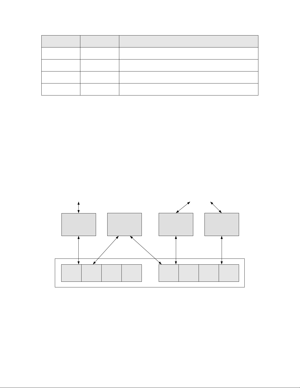
Title Part Number Description
FT 6000 EVB Hardware Guide 078-0504-01A This manual describes the hardware
ONWORKS devices. All of these manuals are available from the
ONWORKS devices and LONWORKS networks. The table
).
Table 1. Related Documentation
for the FT 6000 EVB evaluation
boards that are included with the FT
6000 EVK.
FT 6000 EVB Schematic 012-1460-51A This document provides the
schematic diagrams for the FT 6000
EVB
iv
Page 5

Title Part Number Description
Introduction to the LONWORKS
Platform
078-0183-01B This manual provides an
introduction to the ISO/IEC 14908
(ANSI/EIA/CEA-709.1 and EN
14908) Control Networking Protocol,
and provides a high-level
introduction to L
ONWORKS
®
networks
and the tools and components that
are used for developing, installing,
operating, and maintaining them.
IzoT NodeBuilder User’s Guide 078-0516-01A This manual describes how to
develop L
ONWORKS devices and
applications using the IzoT
NodeBuilder Development Tool.
I/O Model Reference for Smart
Transceivers and Neuron Chips
078-0392-01C This manual provides information
about the I/O models used by
Echelon’s Neuron Chips and Smart
Transceivers.
It includes hardware and software
considerations for each of the I/O
models.
Neuron Assembly Language
Reference
078-0399-01B This manual describes the Neuron
assembly language and how to write
Neuron assembly language functions.
Neuron C Programmer’s Guide 078-0002-01I This manual describes how to write
programs using the Neuron C
Version 2.2 programming language.
Neuron C Reference Guide 078-0140-01G This manual provides reference info
for writing programs using the
Neuron C Version 2.2 programming
language.
IzoT BACnet Developer’s Guide 078-0507-01A This manual details how to develop a
BACnet/IP application on a Series
6000 device.
NodeLoad User’s Guide 078-0286-01G This manual details the uaage of the
NodeLoad application.
NodeUtil User’s Guide 078-0438-01B This manual details the uaage of the
NodeUtil application.
For information about previous generation Smart Transceivers, see the Echelon FT 3120 /
FT 3150 Smart Transceiver Data Book or the Series 5000 Chip Data Book.
Series 6000 Chip Data Book v
Page 6

All of the Echelon product documentation is available in Adobe® PDF format. To view the
PDF files, you must have a current version of the Adobe Reader
. Most Echelon products
include the English-language version of the Adobe Reader; you can download other language
versions from Adobe at: www.adobe.com/products/acrobat/readstep2.html
.
Standards Documents Referenced in this Manual
This manual refers to the following standards documents:
• American Society for Testing and Materials (ASTM) B258 - 02(2008) Standard
Specification for Standard Nominal Diameters and Cross-Sectional Areas of AWG
Sizes of Solid Round Wires Used as Electrical Conductors.
www.astm.org/Standards/B258.htm
• Comité européen de normalisation electrotechnique
Information technology equipment – Radio disturbance characteristics – Limits and
methods of measurement.
• Comité international spécial des perturbations radioélectriques
Information Technology Equipment – Radio Disturbance Characteristics – Limits
and Methods of Measurement.
1
(CENELEC) EN 55022 –
2
(CISPR) 22 –
• Electrostatic Discharge Association standard ESD STM5.1: Electrostatic Discharge
Sensitivity Testing – Human Body Model. www.esda.org/freedowloads.html
• European Union Restriction of Hazardous Substances (RoHS) Directive 2002/95/EC.
europa.eu.int/eur-lex/pri/en/oj/dat/2003/l_037/l_03720030213en00190023.pdf
• Comité européen de normalisation
3
(CEN) Electromagnetic Compatibility (EMC)
standards (see Table 2).
• International Organization for Standardization (ISO) and International
Electrotechnical Commission (IEC) standard ISO/IEC 14908 Control Network
Protocol
• Institute of Electrical and Electronics Engineers (IEEE) Standard Test Access Port
and Boundary-Scan Architecture (IEEE 1149.1-1990).
www.ieee.org/web/standards/home/index.html
.
• Institute for Printed Circuits (IPC) / Joint Electron Device Engineering Council
(JEDEC) Solid State Technology Association standard: IPC/JEDEC J-STD-020D.1 –
Moisture/Reflow Sensitivity Classification for Nonhermetic Solid State Surface
Mount Devices. www.jedec.org/download/search/JSTD020D-01.pdf
• Title 47 of the Code of Federal Regulations (CFR) Part 15, Radio Frequency Devices.
www.fcc.gov/oet/info/rules/
• US Military Standard MIL-STD-883 Test Method Standard, Microcircuits: Method
3015.7, Electrostatic Discharge Sensitivity Classification.
1
European Committee for Electrotechnical Standardization
2
International Special Committee on Radio Interference
3
European Committee for Standardization
vi
Page 7

You can purchase copies of CENELEC documents, IEC EMC standards, ISO standards, US
Military Standards, and CISPR documents from the Information Handling Services (IHS)
Global page at: global.ihs.com
www.iec.ch.
Table 2. IEC Electromagnetic Compatibility (EMC) Standards
Standard Title
IEC 61000-4-1 Electromagnetic compatibility (EMC) - Part 4-1: Testing and
measurement techniques - Overview of IEC 61000-4 series
IEC 61000-4-2 Electromagnetic compatibility (EMC) - Part 4-2: Testing and
measurement techniques - Electrostatic discharge immunity test
IEC 61000-4-3 Electromagnetic compatibility (EMC) - Part 4-3 : Testing and
measurement techniques - Radiated, radio-frequency, electromagnetic
field immunity test
. IEC EMC standards are also available from the IEC at:
IEC 61000-4-4 Electromagnetic compatibility (EMC) - Part 4-4: Testing and
measurement techniques - Electrical fast transient/burst immunity test
IEC 61000-4-5 Electromagnetic compatibility (EMC) - Part 4-5: Testing and
measurement techniques - Surge immunity test
IEC 61000-4-6 Electromagnetic compatibility (EMC) - Part 4-6: Testing and
measurement techniques - Immunity to conducted disturbances, induced
by radio-frequency fields
Series 6000 Chip Data Book vii
Page 8

Table of Contents
Welcome ......................................................................................................... iii
Audience ........................................................................................................ iii
What’s New for Echelon’s Smart Transceivers and Neuron Chips ........... iii
Related Documentation ................................................................................ iv
Standards Documents Referenced in this Manual ..................................... vi
Introduction ....................................................................................................... 1
Product Family Overview .............................................................................. 2
FT 6000 Smart Transceiver .................................................................... 2
Neuron 6000 Processor ............................................................................ 2
Development Resources for Series 6000 Chips ............................................ 2
Introduction to LONWORKS Networks .......................................................... 3
Overview of the IzoT Platform ...................................................................... 4
Overview of Free Topology Technology ........................................................ 5
Key Features of Series 6000 Chips ............................................................... 8
Additional Key Features for FT 6000 Smart Transceivers................... 8
Specification Summaries ............................................................................... 9
Specification Summary for FT 6000 Smart Transceivers ..................... 9
Specification Summary for Neuron 6000 Processors .......................... 11
Hardware Resources ...................................................................................... 13
Series 6000 Architecture ............................................................................. 14
Neuron Processor Architecture ............................................................. 15
Multiple Processors ............................................................................... 17
Interrupts ............................................................................................... 19
Assembly Instruction Set ...................................................................... 19
Memory Architecture ................................................................................... 23
On-Chip Memory ................................................................................... 24
Memory Map .......................................................................................... 24
External Serial Memory Interface ........................................................ 26
Serial Peripheral Interface (SPI) ................................................... 26
Non-Volatile Memory Integrity ...................................................... 27
Device Support ................................................................................ 28
Device Programming....................................................................... 29
Recovering a Device ........................................................................ 29
Transience .............................................................................................. 30
Data Logging .......................................................................................... 30
Boot Loader ............................................................................................ 30
JTAG Interface ............................................................................................. 31
Operating Conditions ................................................................................... 32
Pin Assignments .......................................................................................... 34
FT 6000 Smart Transceiver .................................................................. 34
Neuron 6000 Processor .......................................................................... 36
Pin Connections ............................................................................................ 39
Characteristics of the Digital Pins .............................................................. 43
Communications Port (CP) Pins for the Neuron 6000 Processor .............. 44
Single-Ended Mode ................................................................................ 46
Collision Detection for Single-Ended Mode ................................... 48
Beta 1 and Beta 2 Timeslots in Single-Ended Mode .................... 48
Special-Purpose Mode ........................................................................... 50
Network Connection .................................................................................... 54
Connection for an FT 6000 Smart Transceiver ................................... 54
viii
Page 9

Comparison with FT 3120 or FT 3150 Devices ............................. 55
Comparison with Series 5000 Devices ........................................... 56
Comparison with the FTT-10A Transceiver .................................. 56
Connection for a Neuron 6000 Processor ............................................. 57
TPT/XF-1250 Transceivers ............................................................. 57
EIA-485 Transceivers ..................................................................... 58
LPT-11 Link Power Transceivers .................................................. 59
Clock Requirements ..................................................................................... 61
External Crystal .................................................................................... 61
Comparison with Series 3100 Clocks ................................................... 62
Reset Function.............................................................................................. 63
RST~ Pin ................................................................................................ 63
Reset Sources ......................................................................................... 64
Power-Up and LVI .......................................................................... 65
Watchdog Timer .............................................................................. 65
Traps ................................................................................................ 66
Software-Controlled Reset .............................................................. 66
Reset Processes and Timing ................................................................. 66
SVC~ Pin ...................................................................................................... 69
Integrity Mechanisms .................................................................................. 70
Processor Integrity ................................................................................ 70
System Firmware Image ....................................................................... 70
Application Integrity Using Checksums .............................................. 70
Hardware Design Considerations ............................................................... 73
PC Board Layout Guidelines ....................................................................... 74
Design and Test for Electromagnetic Compatibility ............................. 77
Overview ....................................................................................................... 78
Achieving High Immunity ........................................................................... 79
Electrostatic Discharge ................................................................................ 79
Electromagnetic Interference ...................................................................... 80
Radiated and Conducted Immunity ............................................................ 82
Surge and Burst ........................................................................................... 85
Lightning Protection .................................................................................... 86
Building Entrance Protection ............................................................... 86
Network Line Protection ....................................................................... 86
Shield Protection ................................................................................... 86
Suggested Gas Discharge Arresters ..................................................... 86
Avoiding Magnetic Field Interference ........................................................ 88
Summary and Testing Results .................................................................... 89
Network Cabling and Connections for FT Devices ................................ 91
Network Connection .................................................................................... 92
Network Topology Overview ....................................................................... 92
System Performance and Cable Selection .................................................. 94
System Specifications ............................................................................ 95
Transmission Distance Specifications .................................................. 95
Cable Termination and Shield Grounding ................................................. 96
Free Topology Network Segment ......................................................... 96
Doubly Terminated Bus Topology Segment ........................................ 96
Grounding Shielded Twisted Pair Cable .............................................. 97
Input/Output Interfaces for the Series 6000 ............................................ 99
Overview ..................................................................................................... 100
Series 6000 Chip Data Book ix
Page 10

Two 16-Bit Timer/Counters ....................................................................... 100
Summary of the Available I/O Objects ..................................................... 101
Hardware Considerations .......................................................................... 109
Programming Considerations.................................................................... 113
Application Program Development ........................................................... 114
IzoT NodeBuilder Development Tool ........................................................ 114
Development Hardware Setup ........................................................... 114
Release Hardware Setup ..................................................................... 115
SNMP Support ........................................................................................... 116
Supported Commands ......................................................................... 116
Supported Objects ................................................................................ 116
Migrating from earlier Neuron Chips ....................................................... 117
Migrating Self-Installation Routines ................................................. 117
Series 6000 Design Checklists .................................................................... 119
Checklist 1: Series 6000 Chip Connections .............................................. 120
Checklist 2: FT 6000 Smart Transceiver Connections ............................ 122
Checklist 3: Neuron 6000 Processor Connections .................................... 123
Checklist 4: Power Supply ......................................................................... 124
Checklist 5: Device PCB Layout ............................................................... 125
Checklist 6: Network Cabling and Termination ...................................... 126
Checklist 7: Device Programming ............................................................. 127
Qualified TP/FT-10 Cable Specifications ................................................ 129
Introduction ................................................................................................ 130
Qualified Cables ......................................................................................... 130
Category 5 and 6 Cable Specifications ............................................... 131
NEMA Type 4 Cable Specifications .................................................... 131
16 AWG (1.3 mm) “Generic” Cable Specifications ............................. 133
FT-X3 Communications Transformer ...................................................... 135
Transformer Pinout ................................................................................... 136
Transformer Electrical Connections ......................................................... 137
Transformer Pad Layout ........................................................................... 138
Handling and Manufacturing Guidelines ............................................... 141
Application Considerations ....................................................................... 142
Termination of Unused Pins ............................................................... 142
Avoidance of Damaging Conditions .................................................... 143
Electrostatic Discharge Design Guidelines ........................................ 145
Power Supply, Ground, and Noise Considerations ........................... 145
Decoupling Capacitors ......................................................................... 146
Board Soldering Considerations ............................................................... 146
Recommended Solder Profile .............................................................. 146
Soldering Surface Mount (SMT) Parts ............................................... 147
General ESD Handling Guidelines ........................................................... 147
Power Distribution and Decoupling Capacitors ....................................... 151
Recommended Bypass Capacitor Placement ............................................ 151
Example Schematic ...................................................................................... 155
Example Schematic .................................................................................... 156
Basic Electrical Connections ............................................................... 156
Memory Interface Connections ........................................................... 157
Transformer Connections .................................................................... 157
x
Page 11

I/O and Network Connections ............................................................. 157
BOM for Example Schematic .................................................................... 158
Vendor Contact Information ...................................................................... 160
Vendor Information .................................................................................... 161
Abracon Corporation ........................................................................... 161
Atmel Corporation ............................................................................... 161
Belden Inc. ........................................................................................... 161
BPM Microsystems .............................................................................. 162
Citel Inc. ............................................................................................... 162
CommScope Inc. ................................................................................... 162
Emulation Technology Inc. ................................................................. 163
Fairchild Semiconductor Inc. .............................................................. 163
HiLo System Research Company Ltd. ............................................... 163
Laird Technologies PLC ...................................................................... 164
Littelfuse Inc. ....................................................................................... 164
Numonyx BV ........................................................................................ 164
NXP Semiconductors BV ..................................................................... 165
ON Semiconductor ............................................................................... 165
Panasonic Corp. ................................................................................... 165
Plastronics Socket Company Inc. ....................................................... 166
Sankosha Corp. .................................................................................... 166
Silicon Storage Technology Inc. .......................................................... 166
Taiyo Yuden Company Ltd. ................................................................ 167
TDK Corp. ............................................................................................ 167
Total Phase Inc. ................................................................................... 167
Vishay Intertechnology Inc. ................................................................ 168
Series 6000 Chip Data Book xi
Page 12

Page 13

Introduction
This chapter introduces the Series 6000 of products,
ONWORKS networks, and free topology networking.
L
1
Series 6000 Chip Data Book 1
Page 14

Product Family Overview
Echelon designed the original Neuron Chip as a system-on-a-chip semiconductor device to
provide intelligence and networking capabilities to low-cost control devices. Through a
unique combination of hardware and firmware, the Neuron Chip provided all of the key
functions necessary to process inputs from sensors and control devices intelligently, and to
propagate control information across a variety of network media. Since then, Echelon has
continued to develop and improve the families of products that are based on the Neuron
Chip.
This book describes the newest additions to the Neuron families of products:
• FT 6000 Free Topology Smart Transceivers
• Neuron 6000 Processors
This book describes these products generically as “Series 6000 chips”.
All Series 6000 chips include multiple processors, read-write and read-only memory (RAM
and ROM), communication subsystems, and I/O subsystems. Each Series 6000 chip includes
a processor core for running applications and managing network communications, memory,
I/O, and a 48-bit identification number (the Neuron ID) that is unique to every device. In
addition, all Series 6000 chips include the Neuron system firmware, which provides an
implementation of the LonTalk
application-program management. The device manufacturer provides the application code
and the I/O devices that complete a L
®
protocol, along with I/O libraries, and a task scheduler for
ONWORKS device.
The Neuron 6000 Processor provides a media-independent communications port which
permits short distance Neuron Chip-to-Neuron Chip communications, and can also be used
with external line drivers and transceivers of almost any type.
FT 6000 Smart Transceiver
The FT 6000 Free Topology Smart Transceiver integrates a high performance Neuron core
with a free topology twisted pair transceiver. Together with the FT-X3 Communications
Transformer and inexpensive serial memories, the FT 6000 Smart Transceiver provides a
low-cost, high-performance solution.
Neuron 6000 Processor
The Neuron 6000 Processor provides a media-independent communications port that
supports external transceivers for EIA-485 or TP/XF-1250 channels, using an external
transceiver circuit. The Neuron 6000 Processor can also connect to a link-power TP/FT-10
channel using a L
provides a lower-cost, higher-performance alternative to the previous generation of Neuron
Chips.
ONWORKS LPT-11 Link Power Transceiver. The Neuron 6000 Processor
Development Resources for Series 6000 Chips
A wide assortment of technical documentation, diagnostic tools, support programs, and
training courses are available to assist customers with their projects. Additionally, Echelon
offers fee-based pre-production design reviews of customers’ products, schematics, PCB
layouts, and bills of material to verify that they comply with published guidelines.
2 Introduction
Page 15

Introduction to LONWORKS Networks
In almost every industry, there is a trend away from proprietary control schemes and
centralized systems. The migration towards open, distributed, peer-to-peer networks is
being driven by the need for interoperability, robust technology, faster development time,
and scale economies.
With thousands of application developers and millions of devices installed worldwide, the
ONWORKS system is the leading open solution for building and home automation,
L
industrial, transportation, and public utility control networks. A control network is any
group of devices working in a peer-to-peer fashion to monitor sensors, control actuators,
communicate reliably, manage network operation, and provide complete access to network
data. A L
network data from any device in the network.
ONWORKS network provides communications and complete access to control
The communications protocol used for L
ONWORKS networks is the ISO/IEC 14908-1
(ANSI/CEA 709.1-B and EN14908.1) Control Network Protocol. This protocol is an
international standard seven-layer protocol that has been optimized for control applications
and is based on the Open Systems Interconnection (OSI) Basic Reference Model (the OSI
Model, ISO standard 7498-1). The OSI Model describes computer network communications
through the seven abstract layers described in Table 3. The implementation of these layers
ONWORKS device provides standardized interconnectivity for devices within a
in a L
ONWORKS network.
L
Table 3. L
ONWORKS Network Protocol Layers
OSI Layer Purpose Services Provided
7 Application Application compatibility Network configuration, self-installation,
network diagnostics, file transfer,
application configuration, application
specification, alarms, data logging,
scheduling
6 Presentation Data interpretation Network variables, application messages,
foreign frame transmission
5 Session Control Request/response, authentication
4 Transport End-to-end
communication reliability
Acknowledged and unacknowledged
message delivery, common ordering,
duplicate detection
3 Network Destination addressing Unicast and multicast addressing,
routers
2 Data Link Media access and framing Framing, data encoding, CRC error
checking, predictive carrier sense
multiple access (CSMA), collision
avoidance, priority, collision detection
1 Physical Electrical interconnect Media-specific interfaces and modulation
schemes
Series 6000 Chip Data Book 3
Page 16

Echelon’s implementation of the ISO/IEC 14908-1 Control Network Protocol is called the
LonTalk protocol. Echelon provides implementations of the LonTalk protocol with several
product offerings, including the Neuron system firmware, OpenLNS
client, SmartServers,and the ShortStack
ISO/IEC 14908-1 Control Network Protocol as the “LonTalk protocol”, although other
interoperable implementations exist.
ONWORKS system is based on the following concepts:
A L
• Control systems have many common requirements regardless of application.
• A networked control system is significantly more powerful, flexible, and scalable than
a non-networked control system.
• Businesses can save and make more money with control networks over the long term
than they can with non-networked control systems.
L
ONWORKS networks provide a complete suite of messaging services, including end-to-end
acknowledgement, authentication, and priority message delivery. Network management
services allow network tools to interact with devices over the network, including local or
remote reconfiguration of network addresses and parameters, downloading of application
programs, reporting of network problems, and start/stop/reset of device application
programs.
ONWORKS networks range in sophistication from small networks embedded in machines to
L
large networks with thousands of devices controlling fusion lasers, paper manufacturing
machines, or building automation systems. L
trains, airplanes, factories, and hundreds of other processes. Manufacturers are using open,
off-the-shelf chips, operating systems, and parts to build products that feature improved
reliability, flexibility, system cost, and performance.
®
Micro Server. This document refers to the
ONWORKS networks are used in buildings,
®
Server, LNS remote
Echelon manufactures many L
and end users implement L
ONWORKS solution including development tools, network management software, power line
L
and twisted pair transceivers and control modules, network interfaces, technical support and
training.
See Introduction to the LonWorks Platform (078-0183-01B) for more information about
ONWORKS networks.
L
ONWORKS products to help developers, system integrators,
ONWORKS networks. These products provide a complete
Overview of the IzoT Platform
The IzoT™ Platform is an IP-enabled family of chips, stacks, interfaces, and
management software that enables the development of devices, peer-to-peer device
communities, and applications for the Industrial Internet of Things. Unlike consumergrade platforms, the IzoT Platform comprehensively addresses unique IIoT requirements
such as autonomous control, multi-cast addressing and industrial-strength reliability.
The IzoT platform builds on LonWorks networking technology by adding native IP
support down to individual field devices, with Neuron 6050 and FT 6050 based devices
providing the option of backwards compatibility with ISO/IEC 14908-1.
4 Introduction
Page 17

Series 6000 based field devices are capable of running multiple protocols (LonTalk,
LonTalk/IP, BACnet/IP, SNMP, ICMP with UDP sockets available) with a variety of
transceiver options.
Overview of Free Topology Technology
A conventional control system using bus topology wiring (such as an EIA-485 network)
consists of a network of sensors and actuators that are interconnected using a twisted wire
pair. In accordance with EIA-485 guidelines, all of the devices must be wired in a bus
topology to limit electrical reflections and to ensure reliable communications. There is a high
cost associated with installing and maintaining the cable plant that links together the
devices of an EIA-485-based control system. Bus topology wiring is more time consuming
and expensive to install, because the installer is unable to branch or star the wiring where
convenient. All devices must be connected directly to the main bus.
The best solution to reduce installation and maintenance costs and to simplify system
modifications is to use a free topology communications system. Echelon’s free topology
transceiver technology offers such a solution, providing an elegant and inexpensive method
of interconnecting the different elements of a distributed control system.
A free topology architecture allows the installer to wire the control devices with virtually no
topology restrictions. Power is supplied by a local DC power supply located at each device as
shown in Figure 1.
Series 6000 Chip Data Book 5
Page 18
Smart
Transceiver
Smart
Transceiver
Smart
Transceiver
Smart
Transceiver
Smart
Transceiver
Smart
Transceiver
Termination
To Additional
Free Topology
Devices
Sensor
Actuator
DC power
Smart Transceivers
:
•
FT
3120
Smart Transceiver
•
FT
3150 Smart Transceiver
•
FT
5000
Smart Transceiver
•
FT
6000
Smart Transceiver
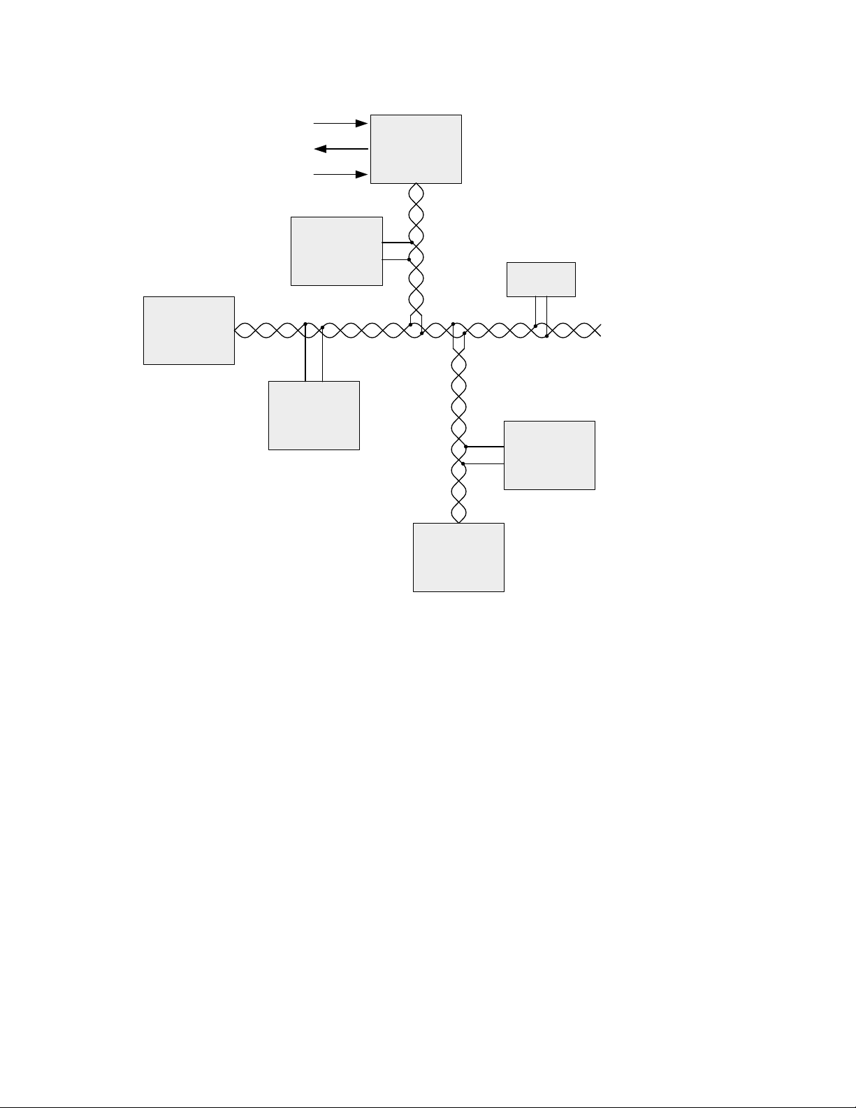
Unlike bus wiring designs, the free topology FT Smart Transceivers or Neuron Chips with
associated transceivers use a wiring scheme that supports star, loop, or bus wiring (see
Figure 2).
Figure 1. Free Topology Transceiver System
6 Introduction
Page 19
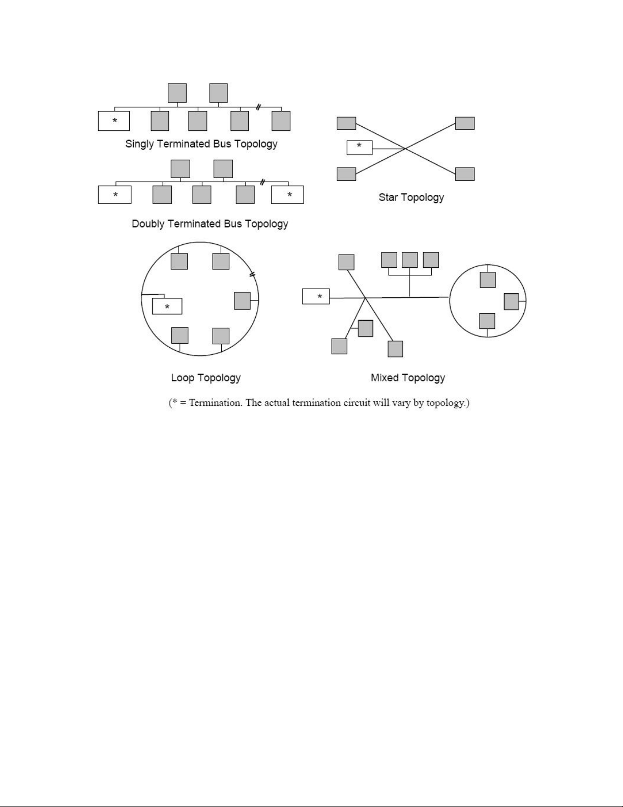
Figure 2. Typical Wiring Topologies Supported by FT Smart Transceivers
This design has many advantages:
• The installer is free to select the method of wiring that best suits the installation,
reducing the need for advanced planning and allowing last minute changes at the
installation site.
• If installers have been trained to use one style of wiring for all installations, free
topology technology can be introduced without requiring retraining.
• Retrofit installations with existing wiring plants can be accommodated with minimal,
if any, rewiring. This capability ensures that FT Smart Transceiver technology can
be adapted to both old and new projects.
• Free topology permits FT Smart Transceiver or Neuron Chip systems to be expanded
in the future by simply tapping into the existing wiring where it is most convenient
to do so. This reduces the time and expense of system expansion, and from the
customer's perspective, keeps down the life-cycle cost of the free topology network.
Series 6000 Chip Data Book 7
Page 20

Key Features of Series 6000 Chips
Series 6000 chips include the following key features:
• Provide a high performance Neuron Core, with internal system clock rates up to 80
MHz
• Require as little as 30 mW of power for operations
• Packaged as a 7 mm by 7 mm 48-pin quad flat no leads (QFN) chip
• Include a serial memory interface for inexpensive external flash non-volatile memory
• Support up to 254 network variables (NVs) for FT 6000 Smart Transceivers and
Neuron 6000 Processors, without the need for a host microprocessor
• Support user-programmable interrupts to provide fast response time to external
events
• Provide an interface for the Institute of Electrical and Electronics Engineers (IEEE)
Standard Test Access Port and Boundary-Scan Architecture (IEEE 1149.1-1990) of
the Joint Test Action Group (JTAG) to allow a Series 6000 chip to be included in the
boundary-scan chain for device production tests
• Include 12 I/O pins with 35 programmable standard I/O models that support both 5 V
and 3.3 V I/O operation
• Support up to 256 KB of user application code space (with a 1MB external flash)
• Include 64 KB RAM (of which 44 KB is user accessible) and 16 KB of ROM on-chip
• Include a unique 48-bit MAC ID in every device for network installation and
management
• Support a –40°C to +85°C operating temperature range
• Compliant with the European Union Restriction of Hazardous Substances (RoHS)
Directive 2002/95/EC.
Additional Key Features for FT 6000 Smart Transceivers
FT 6000 Smart Transceivers include the following additional key features:
• Support polarity insensitive free topology star, daisy chain, bus, loop, or mixed
topology wiring for TP/FT-10 channels
• Compliant with TP/FT-10 channels that currently use FT 3120 Smart Transceivers,
FT 3150 Smart Transceivers, FTT-10A transceivers, LPT-11 transceivers or FT-5000
Transceivers
• Provide very high common-mode noise immunity
8 Introduction
Page 21

Specification Summaries
The following sections summarize the specifications for FT 6000 Smart Transceivers and
Neuron 6000 Processors.
Specification Summary for FT 6000 Smart Transceivers
Table 4 summarizes the specifications for the FT 6000 Smart Transceiver.
Table 4. FT 6000 Smart Transceiver Specification Summary
Description Specification
Data communications type Differential Manchester encoding
Transmission speed 78 kilobits per second
Network polarity Polarity insensitive
Number of transceivers per network
segment
Network wiring 24 to 16 AWG twisted pair
Network length for free topology Varies by wire type.
Network length for bus topology Varies by wire type.
Maximum stub length for bus
topology
Network termination One terminator for free topology
Up to 64
• Up to 1000 m (3280 ft) maximum total wire
with one repeater
• Up to 500 m (1640 ft) maximum total wire
with no repeaters
• 5400 m (17 710 ft) maximum total wire with
one repeater
• 2700 m (8850 ft) maximum total wire with no
repeaters
3 m (9.8 ft)
Two terminators for bus topology
Voltage for FT 6000 Smart
Transceiver
Operating temperature –40 ºC to +85 ºC
Series 6000 Chip Data Book 9
3.3 V ±5%
Page 22

Description Specification
Reflow soldering temperature profile Refer to Joint Industry Standard document
IPC/JEDEC J-STD-020D.1 (March 2008)
Peak reflow soldering temperature 260 ºC
Package type 48-pin QFN
RoHS compliant Yes
EMI
ESD Designed to comply with EN 61000-4-2, Level 4
Radiated Electromagnetic
Susceptibility
Fast Transient/Burst Immunity Designed to comply with EN 61000-4-4, Level 4
Surge Immunity Designed to comply with EN 61000-4-5, Level 3
Conducted RF Immunity Designed to comply with EN 61000-4-6, Level 3
Table 5 summarizes the specifications for the FT-X3 Communications Transformer.
Table 5. FT-X3 Communications Transformer Specification Summary
Description Specification
Operating humidity 25-90% RH @50 °C, non-condensing
Non-operating humidity 95% RH @ 50 °C, non-condensing
Designed to comply with FCC Part 15 Subpart B and
EN 55022 Level B
Designed to comply with EN 61000-4-3, Level 3
Vibration 1.5 g peak-to-peak, 8 Hz to 2 kHz
Mechanical shock 100 g (peak)
Reflow soldering temperature profile Refer to Joint Industry Standard document
IPC/JEDEC J-STD-020D.1 (March 2008)
Peak reflow soldering temperature 245 ºC
10 Introduction
Page 23

Specification S ummary for Neuron 6000 Processors
Table 6 summarizes the specifications for the Neuron 6000 Processor.
Table 6. Neuron 6000 Processor Specification Summary
Description Specification
Transmission speed Depends on network transceiver:
• 78 kbit/s for TP/FT-10 channel
• 1250 kbit/s for TP/XF-1250 channel
• See EIA-485 channel specification for
transmission speed characteristics
Voltage for Neuron 6000 Processor 3.3 V ±10%
Operating temperature –40 ºC to +85 ºC
Reflow soldering temperature profile Refer to Joint Industry Standard document
IPC/JEDEC J-STD-020D.1 (March 2008)
Peak reflow soldering temperature 260 ºC
Package type 48-pin QFN
RoHS compliant Yes
EMC Depends on network transceiver
Series 6000 Chip Data Book 11
Page 24

Page 25

2
Hardware Resources
This chapter provides an overview of the hardware resources
for an FT 6000 Smart Transceiver and a Neuron 6000
Processor, including the overall chip architecture, memory
interface, operating parameters, pinouts, network
connection, clock requirements, the reset function, and
integrity mechanisms.
Series 6000 Chip Data Book 13
Page 26

Series 6000 Architecture
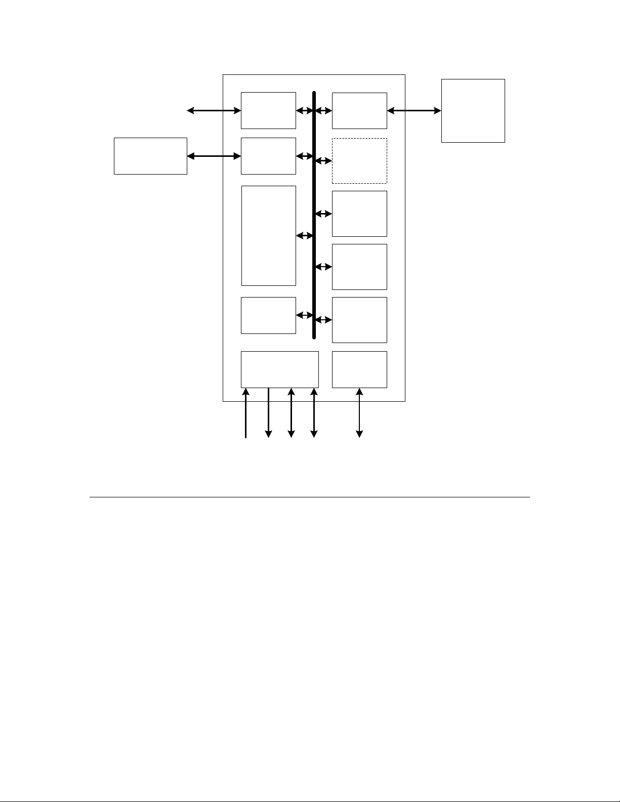
The main components of the architecture for a Series 6000 chip, as shown in Figure 3
include:
• CPUs — a Series 6000 chip includes three processors to manage operation of the
chip, the network, and the user application. At higher clock rates, there is also a
separate processor to handle interrupts.
• ROM — a Series 6000 chip includes 16 KB of read-only memory (ROM), which holds
the a system firmware image used for booting a system image from flash.
• RAM — a Series 6000 chip includes 64 KB of random access memory (RAM), which
stores user applications and data. The RAM is partitioned according to a logical
memory map so that the amount that is available for user applications and data is
less than 64 KB. See Memory Map for information about how the RAM is configured.
• Serial memory interface — this interface manages the external non-volatile memory
(NVM) using the serial peripheral interface (SPI).
• Communications port — the communications port provides network access for the
chip. For an FT 6000 Smart Transceiver, this port connects to an FT-X3
Communications Transformer. For a Neuron 6000 Processor, this port connects to an
external transceiver.
• I/O — 12 dedicated I/O pins (see Characteristics of the Digital Pins).
• Clock, reset, and service — on-chip clock, phase-locked loop (PLL), reset, and service-
pin functions.
• JTAG — a Series 6000 chip includes a JTAG (IEEE 1149.1) interface for boundary
scan operations. See JTAG Interface.
The pinout labels shown in Figure 3 are described in Pin Assignments.
14 Hardware Resources
Page 27
Clock, Reset,
and Service
Serial
Memory
Interface
RAM
(64K x
8
)
I
/
O
Comm
Port
NET CPU
Transformer
or
transceiver
NVM
(
SPI
)
ROM
(16
K x 8
)
JTAG
APP CPU
IRQ CPU
MAC
CPU
XIN
XOUT
RST~
/
/
/
/
12
5
5
6
SVC~
Neuron Processor Architecture
The basic Neuron processor architecture is stack-oriented:
• An 8-bit-wide stack is used for data references, and the arithmetic-logic unit (ALU)
• Another stack stores the return addresses for CALL instructions, and can also be
This stack architecture leads to very compact code. See Assembly Instruction Set for a
summary of the instruction set.
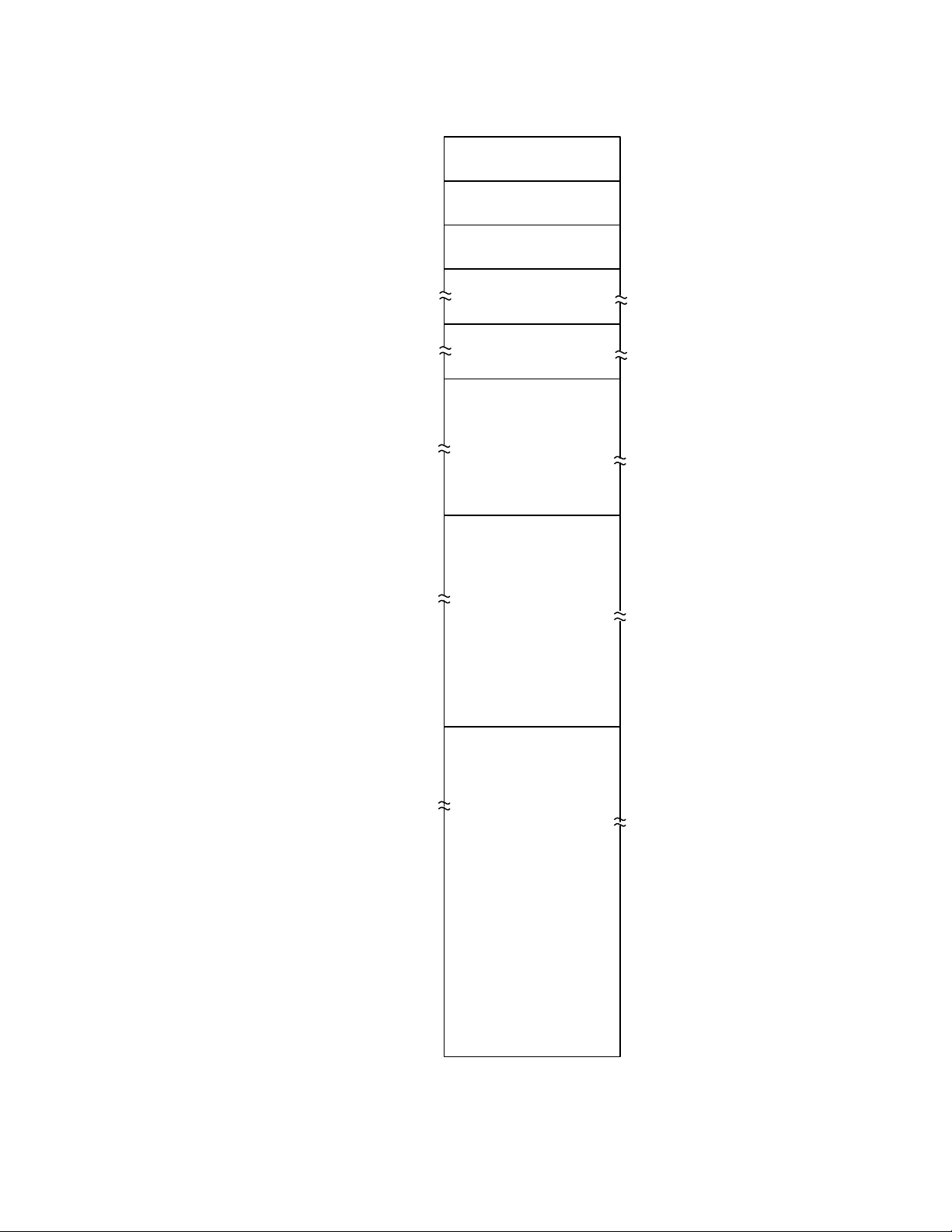
Figure 4 shows the layout of a base page, which can be up to 256 bytes long. Each of the
chip’s processors uses a different base page, whose address is given by the contents of the BP
(Base Page) register of that processor. The top of the data stack is in the 8-bit TOS register,
and the next element in the data stack is at the location within the base page at the offset
given by the contents of the DSP (Data Stack Pointer) register. The assembler shorthand
operates on the TOS (Top of Stack) register and on the next entry in the data stack
(which is in RAM).
used for temporary data storage.
Figure 3. Series 6000 Chip Architecture
Series 6000 Chip Data Book 15
Page 28
symbol NEXT refers to the next element in the data stack, which is determined by contents
of the location (BP+DSP) in memory, and is thus not an actual processor register.
Figure 4. Base-Page Memory Layout
The data stack grows from low memory towards high memory, and is managed through the
DSP (Data Stack Pointer) register. Pushing a byte of data onto the data stack involves the
following steps:
1. Incrementing the DSP register
2. Storing the current contents of TOS at the address (BP+DSP) in memory
3. Moving the byte of data to TOS
Popping a byte of data from the data stack involves the following steps:
1. Moving TOS to the destination
2. Moving the contents of the address (BP+DSP) in memory to TOS
3. Decrementing the DSP register
The return stack grows from high memory towards low memory, and is managed through the
RSP (Return Stack Pointer) register. Calling a subroutine involves the following steps:
1. Storing the high byte of the instruction pointer (IP) register at the address (BP+RSP)
in memory
2. Decrementing RSP
3. Storing the low byte of IP at the address (BP+RSP) in memory
4. Decrementing RSP
5. Moving the destination address to the IP register
Similarly, returning from a subroutine involves the following steps:
16 Hardware Resources
Page 29

1. Incrementing RSP
2. Moving the contents of (BP+RSP) to the low byte of the IP register
3. Incrementing RSP
4. Moving the contents of (BP+RSP) to the high byte of IP
The primary programming language used for applications is the Neuron C language, which
is a derivative of the ANSI C language that has been optimized and enhanced for L
distributed control applications. The major enhancements include:
• A network communication model, based on functional blocks and network variables,
that simplifies and promotes data sharing between like and disparate devices.
• A network configuration model, based on functional blocks and configuration
properties, that facilitates interoperable network configuration tools.
• A type model based on standard and user resource files that expands the market for
interoperable devices by simplifying the integration of devices from multiple
manufacturers.
• An extensive set of I/O models that support the I/O capabilities of Neuron Chips and
Smart Transceivers.
• Powerful event-driven programming extensions, based on when statements, that
provide easy handling of network, I/O, and timer events.
ONWORKS
• A high-level programming model that supports application-specific interrupt
handlers and synchronization tools.
See the Neuron C Programmer’s Guide for more information about the Neuron C
programming language. The support for these capabilities is part of the Neuron firmware,
and does not need to be written by the programmer.
Multiple Processors
The Neuron core is composed of four independent logical processors:
• Processor 1 is the Media Access Control (MAC) processor
• Processor 2 is the network (NET) processor
• Processor 3 is the application (APP) processor
• Processor 4 is the interrupt (ISR) processor
The interrupt processor is only available for system clock rates of 20 MHz and higher. At the
two lower system clock rates, interrupts are handled by the application processor. See
Interrupts for more information about interrupts.
The processors share a common memory, arithmetic-logic unit (ALU), and control circuitry.
Each processor has its own set of registers, as listed in Table 7.
Table 7. Register Set
Register Size (Bits) Contents
FLAGS 8 Carry Bit and reserved internal flags
IP 16 Next Instruction Pointer
Series 6000 Chip Data Book 17
Page 30
MAC
Processor
Network
Processor
Application
Processor
Interrupt
Processor
Shared
Network Buffers Application Buffers
Communications
Port
Input/Output
Register Size (Bits) Contents
BP 16 Address of 256-Byte Base Page
DSP 8 Data Stack Pointer within Base Page
RSP 8 Return Stack Pointer within Base Page
TOS 8 Top of Data Stack, ALU Input
Processor 1 is the MAC layer processor that handles layers 1 and 2 of the seven-layer
®
LonTalk
protocol, which includes driving the communications subsystem hardware and
running the media access control algorithm. The MAC processor communicates with the
NET processor using network buffers located in shared RAM memory, as shown in Figure 5.
Processor 2 is the network processor that implements layers 3 through 6 of the LonTalk
protocol. The NET processor handles network variable processing, addressing, transaction
processing, authentication, background diagnostics, software timers, network management,
and routing functions. The NET processor uses network buffers in shared memory to
communicate with the MAC processor, and application buffers to communicate with the APP
processor. These buffers are also located in shared memory (RAM). Access to the shared
memory is mediated with hardware semaphores to resolve contention when updating shared
data.
Processor 3 is the application processor. The APP processor executes the user-written code,
together with the system services called by user code.
Figure 5. Processor Shared Memory Allocation
18 Hardware Resources
Page 31

(
)
kSystemCloc
clesNumberOfCy
nTimeInstructio
3×
=
Interrupts
The Series 6000 architecture provides hardware support for handling three types of
interrupts:
• Lowest priority: application interrupts
• Medium priority: system interrupts
• Highest priority: system-level traps
Application interrupts are asynchronous events related to I/O objects within an application
program. An application uses the Neuron C interrupt() clause to define the interrupt
condition and the interrupt task that handles the condition. The Neuron C program runs the
interrupt task whenever the interrupt condition is met. See the Neuron C Programmer’s
Guide for more information about writing interrupt tasks and handling interrupts.
System interrupts are asynchronous system events, such as communications events or SPI
UART events. These interrupts are handled by the system firmware.
System-level traps are also system events, generally error conditions. See Processor Integrity
for more information about these conditions.
For system clock rates of 20 MHz and higher, interrupts are handled by an independent
logical processor within the Neuron Core. At the two lower system clock rates, interrupts are
handled by the application processor. Thus, at the higher clock rates, an interrupt handler
runs in parallel with the application processor, and so does not affect the application
processor’s registers and stack space. At lower clock rates, an interrupt causes a context
switch within the application processor, that is, the interrupt handler saves the processor’s
registers before it runs and restores them after it completes. Thus, the current instruction
always completes prior to servicing a new interrupt. Such context switches also occur within
the ISR processor when higher priority interrupts require service.
Thus, when interrupts are processed within the ISR processor, application performance is
not degraded, but when interrupts are processed within the APP processor, application
performance can be affected because the one processor handles both the application and the
interrupts.
Assembly Instruction Set
Table 8, Table 9, and Table 10 list the processor instructions, their sizes (in bytes), and
their timings (in processor cycles). This information is provided to help you calculate code
sizes and execution times.
Most assembly instructions take between one and seven processor cycles (two instructions
require 14 cycles). Execution time scales inversely with the system clock rate. The formula
for instruction time is:
For example, at a system clock rate of 80 MHz, instruction times vary between 37.5 ns and
175 ns.
Programming for a Neuron Chip or Smart Transceiver uses the Neuron C programming
language with the IzoT NodeBuilder Development Tool. Additional functions can be written
Series 6000 Chip Data Book 19
Page 32

in the Neuron Assembly language. The Neuron C compiler can optionally produce an
assembly listing, and examining this listing can help the programmer to optimize the Neuron
C source code. See the Neuron Assembly Language Reference for more information about the
processor instructions.
Table 8. Program Control Instructions
Instruction
Size
Instruction
NOP 1 1 No operation
SBR 1 1 Short unconditional branch
BR
BRC
BRNC
SBRZ
SBRNZ
BRF 3 4 Unconditional branch far
BRZ
BRNZ
(Bytes)
2 2 Branch
1 3 Short branch on TOS zero
2 4 Branch on TOS zero
CPU
Cycles
Required Description
Offset: 0 to 15.
Branch on carry
Branch on not carry
Offset: –128 to +127.
Short branch on TOS not zero
Offset: 0 to 15. Drops TOS.
Branch on TOS not zero
Offset: –128 to +127. Drops TOS.
RET 1 5 Return from subroutine.
Drops two bytes from return stack.
BRNEQ 3 4 / 6
(taken /
not taken)
DBRNZ 2 5 Decrement [RSP] and branch if not zero
CALLR 2 5 Call subroutine relative
CALL 2 6 Call subroutine
Branch if TOS not equal
Offset: –128 to +127. Drops TOS if equal.
Offset: –128 to +127. If not taken, drops
one byte from return stack.
Offset: –128 to +127. Pushes two bytes to
return stack.
Address in low 8 KB. Pushes two bytes to
return stack.
20 Hardware Resources
Page 33

Instruction
Size
Instruction
CALLF 3 7 Call subroutine far
Instruction
PUSH TOS 1 3 Increment DSP, duplicate TOS into NEXT
DROP TOS 1 3 Move NEXT to TOS, decrement DSP
DROP_R TOS 1 6 Move NEXT to TOS, decrement DSP,
PUSH NEXT
PUSH DSP
PUSH RSP
PUSH FLAGS
(Bytes)
Table 9. Memory and Stack Instructions
Instruction
Size
(Bytes)
1 4 Push processor register
CPU
Cycles
Required Description
Pushes two bytes to return stack.
CPU
Cycles
Required Description
return from call
POP NEXT
POP DSP
POP RSP
POP FLAGS
DROP NEXT 1 2 Decrement DSP
DROP_R NEXT 1 5 Decrement DSP and return from call
PUSH !D
POP !D
PUSH !TOS 1 4 Push TOS
POP !TOS 1 4 Pop TOS
PUSH [RSP] 1 4 Push from return stack to data stack, RSP
DROP [RSP] 1 2 Increment RSP
1 4 Pop processor register
1 4 Push / pop byte register [8 to 23]
EA = BP + TOS, push byte to NEXT.
EA = BP + TOS, pop byte from NEXT.
unchanged
PUSHS #literal 1 4 Push short literal value [0 to 7]
Series 6000 Chip Data Book 21
Page 34

Instruction
Size
Instruction
PUSH #literal 2 4 Push 8-bit literal value [0 to 255]
PUSHPOP 1 5 Pop from return stack, push to data stack
POPPUSH 1 5 Pop from data stack, push to return stack
PUSH [DSP][-D]
POP [DSP][-D]
PUSHD #literal 3 6 Push 16-bit literal value, high byte first
PUSHD [PTR] 1 6 Push from 16-bit pointer [0 to 3], high byte
POPD [PTR] 1 6 Pop to 16-bit pointer [0 to 3], low byte first
PUSH [PTR][TOS]
POP [PTR][TOS]
(Bytes)
1 5 Push / pop DSP modified by D
1 6 Push / pop 16-bit pointer [0 to 3], modified
CPU
Cycles
Required Description
EA = BP + DSP – displacement [1 to 8]
first
by TOS
EA = (16-bit pointer) + TOS.
PUSH [PTR][D]
POP [PTR][D]
PUSH absolute
POP absolute
Note: EA = Effective Address.
Instruction
INC
DEC
NOT
ROLC
RORC
2 7 Push / pop 16-bit pointer [0 to 3], modified
3 7 Push / pop absolute memory address
Table 10. Arithmetic and Logic Instructions
Instruction
Size
(Bytes)
1 2 Increment TOS
1 2 Rotate left TOS through carry
by D
EA = (16-bit pointer) + displacement [0 to
255]
CPU
Cycles
Required Description
Decrement TOS
Negate TOS
Rotate right TOS through carry
SHL
SHR
22 Hardware Resources
1 2 Unsigned left shift TOS, clear carry
Unsigned right shift TOS, clear carry
Page 35

Instruction
Size
Instruction
SHLA
SHRA
ADD
AND
OR
XOR
ADC
ADD #literal
AND #literal
OR #literal
XOR #literal
ADD_R
AND_R
OR_R
XOR_R
ALLOC #literal 1 3 Add [1 to 8] to data stack pointer
(Bytes)
1 2 Signed left shift TOS into carry
1 4 Operate with NEXT on TOS, drop NEXT
2 3 Operate with literal on TOS
1 7 Operate with NEXT on TOS, drop NEXT
CPU
Cycles
Required Description
Signed right shift TOS into carry
and return
DEALLOC_R
#literal
SUB NEXT,TOS 1 4 TOS = NEXT – TOS, drop NEXT
SBC NEXT, TOS 1 4 TOS = NEXT – TOS – carry, drop NEXT
SUB TOS,NEXT 1 4 TOS = TOS – NEXT, drop NEXT
XCH 1 4 Exchange TOS and NEXT
INC [PTR] 1 6 Increment 16-bit pointer [0 to 3]
DIV 1 14 Divide NEXT by TOS, quotient is in TOS,
MUL 1 14 Multiply NEXT * TOS, result is in TOS,
1 6 Subtract [1 to 8] from data stack pointer
and return
remainder is in NEXT
NEXT
Memory Architecture
The memory architecture for a Series 6000 chip includes on-chip memory and off-chip nonvolatile memory. Every Series 6000 device must have at least 512 KB of off-chip memory
available in an SP1 flash device.
Series 6000 Chip Data Book 23
Page 36

On-Chip Memory
A Series 6000 chip has the following on-chip memory:
• 16 KB of read-only memory (ROM)
The ROM holds an initial system image that is used only to bootstrap the system
from flash or to initially load the flash over the network during manufacturing of a
Series 6000 device. Please see Device Programming for further details.
• 64 KB of random access memory (RAM)
The RAM provides memory for user applications and data, stack segments for each
processor, and network and application buffers. The RAM is partitioned according to
a logical memory map, as described in Memory Map.
A Series 6000 chip contains no internal writable non-volatile memory (such as EEPROM
memory) for application use. However, each Series 6000 chip does contain a unique IEEE
MAC ID in non-volatile read-only memory.
The chip’s memory management block allows the RAM to emulate both ROM and NVM by
ensuring that changes to the RAM are shadowed to external NVM at appropriate intervals.
All writes that are intended for NVM are written to the RAM, and then are shadowed to the
NVM. Thus, the chip’s internal processors access the RAM only; they do not directly access
either the ROM or external NVM.
The state of the RAM is retained as long as power is applied to the device. After a device
reset, the initialization sequence copies the contents of the ROM and relevant NVM data to
the RAM.
Memory Map
A Neuron C application has a memory map of 64 KB. Figure 6 shows the memory map for a
Series 6000 chip. The memory map is a logical view of device memory, rather than a
physical view, because the Series 6000 chip’s processors only directly access RAM.
The memory map for a Series 6000 chip is “auto-tuned”. That is, the linker decides how to
partition the RAM based on the needs placed upon it by the application. The user does not
specify the address ranges used for each type of memory (code vs data vs persistent data).
24 Hardware Resources
Page 37
System and I/O
Network Image
(shadowed to NVM)
Stacks, buffers, app
data
FFFF
F800
F000
E800
Application NVM
(shadowed to NVM)
Application Data
Application and
System Transient
Code
Application Resident
Code
and Constant Data
System Resident
Code, Data and
Constant Data
xx00
xx00
>=D000
__image_end
Series 6000 Chip Data Book 25
Figure 6. Series 6000 Chip Memory Map
Page 38

The memory map divides the Series 6000 chip’s physical RAM into the following types of
logical memory:
• System Image (0x0000 to __image_end (system image dependent)) — This area is
initially a copy of the system firmware image from the physical ROM but this is
overwritten with a system image from flash later in the boot process. This area is
write-protected so that an application cannot alter the system firmware.
• Application Resident Code/Data (from __image_end+1 up to a variable address) —
The size of this area is determined at application link time.
• Transient Code – The size of this area is determined at application link time. By
default, most code in an application is “transient” which means it is brought into this
area from flash on demand. There is some system image transient code as well that
shares this area.
• Application NVM – The size of this area is determined at application link time. The
maximum size of this area is 6KB. This area is brought in from flash at boot time
and written back to flash as it is modified.
• System RAM (2 KB at addresses 0xE800 to 0xEFFF) — This area holds system data,
stack segments, buffers and select application data.
• Mandatory NVM (2 KB at addresses 0xF000 to 0xF7FF) — This area is shadowed
from the mandatory 2 KB of NVM, and holds device configuration data.
• Reserved memory (2 KB at addresses 0xF800 to 0xFFFF) — This area is reserved for
system use.
External Serial Memory Interface
The interface for accessing off-chip non-volatile memory (NVM) is a serial interface that uses
the serial peripheral interface (SPI).
Serial Peripheral Interface (SP I)
The serial peripheral interface (SPI) protocol for the Series 6000 chip uses the pins listed in
table 11 and shown in Figure 7.
Table 11. Memory Interface Pins for the SPI Protocol
Pin
Number
Pin 40 CS0~ Output First slave-select (SS) signal
Pin 43 SDA_CS1~ Bidirectional Second slave-select (SS) signal
Pin 46 MISO Input Master Input, Slave Output (MISO) signal
Pin 47 SCK Output Serial clock (SCK) signal
Pin Name Direction Description
Pin 48 MOSI Output Master Output, Slave Input (MOSI) signal
Note: Signal direction is from the point of view of the Series 6000 chip.
These pins are 3.3 V pins, and are 5 V tolerant.
26 Hardware Resources
Page 39

A Series 6000 chip is always the master SPI device; any external NVM devices are always
slave devices. Multimaster configurations are not supported.
Figure 7. SPI Memory Interface
Series 6000 devices support the 3-byte addressing mode for SPI flash devices.
The SPI protocol defines four modes of operation; each mode specifies different behavior for
flow control on the data bus with respect to the clock signal polarity (CPOL) and phase
(CPHA). A Series 6000 device uses SPI Mode 0: CPOL is 0, CPHA is 0, and the SCK line is
idle low. For this mode, the Series 6000 chip latches in data on the rising edge of the SCK
line, and is output on the falling edge of the SCK line. Note that the 49.9 Ohm and 100k
Ohm resistors shown in the figure are generally not needed, and can be omitted.
A Series 6000 chip runs the SPI protocol from the serial memory interface at 20 MHz for
reads and 2.5 MHz for writes.
Non-Volatile Memory Integrity
The areas labeled Network Image and Application NVM (see Figure 6. Series 6000 Chip
Memory Map) are written out to flash in an all or nothing fashion. This is accomplished by
having multiple copies of the data, an active and a standby. When updating, the standby is
updated and only once that is completed does it become active. Therefore, when changing
NVM from state X to state Y, were a power cycle to occur during the process, you will either
end up in state X or state Y, but not some intermediate (corrupted) version.
The maximum allowed size of this area is 8KB. This means that the typical application nonvolatile data will be limited to somewhere in the range of 6 to 7KB depending on other uses
Series 6000 Chip Data Book 27
Page 40

Command
Value
Write Enable
06h
Read Status Reg
05h
Write Status Reg
01h
Read Data
03h
Page Program (write)
02h
4KB Sector Erase
20h
Chip Erase
C7h
JEDEC ID
9Fh
of this area (e.g., network configuration tables). This area comprises either 2 or 4 flash
sectors of 4KB each depending on the demands of the application. For the 2 sector case, this
area can be modified at most 200,000 times over the device’s lifetime. This works out to
about one update per hour over a 20-year lifetime.
Note that the data is committed to flash using a 500 millisecond hold down timer. So, if you
make multiple modifications to NVM in quick succession, it will typically only result in one
erase/write cycle. Note that if you make modifications to NVM and then do a controlled reset
before the timer expires, the data is written immediately prior to the reset.
Device Support
A Series 6000 device requires 512KB or greater flash devices that meet the requirements as
described below Furthermore, the flash device must use 4KB sectors and be capable of writeprotecting the lower half of the address space.
Larger flash sizes are supported and allow for larger system images and larger application
code, data and logs. Series 6000 chips have no user-accessible on-chip ROM or non-volatile
writable memory. A default system image is contained in on-chip ROM, but its sole purpose
is to support the downloading of the system image over the network in a factory or lab
setting. Flash memory for use with Series 6000 chips must support the following features:
• SPI serial interface, minimum clock rate of 20 MHz
• 24-bit addressing
• At least 4 Mb capacity
• 3.3VCC operation with a minimum 2.7 VCC
• Operating temperature range of -40 °C to +85 °C
• >100,000 erase cycles, 20 year retention data
• Status register with BUSY flag at D0
• 4 KB erasable sector size
• 256-byte page write architecture (up to 256 bytes written inside a single ~CS
assertion
• Block write-protection capability via Status Register write, at least 4 block protect
bits, with capability of protecting first half of the device
• Block write protect setting using these bits: 0bxx1011xx (4 Mb), 0bxx1100xx (8
Mb), 0bxx1101xx (16 Mb), 0bxx1110xx (32 Mb)
• JEDEC ID reporting, including device capacity in the 3
• Identical command set for all implemented commands listed below:
rd
byte
Echelon has qualified the following SPI flash memory devices for use with a Series 6000
device:
28 Hardware Resources
• Winbond W25X40CL 4 M-bit 2.3 V minimum SPI serial flash memory
• Winbond W25Q80BV 8 M-bit 2.7 V minimum SPI serial flash memory
Page 41

• ON Semiconductor LE25U40CMC 4 M-bit 2.3V minimum SPI serial flash memory
• Micron M25PX80 8 M-bit 2.3V minimum SPI serial flash memory
• Macronix MX25L8035E 8 M-bit 2.7V minimum SPI serial flash memory
• Adesto AT25SF041 4 M-bit 2.5V minimum SPI serial flash memory
• Adesto AT25SF081 8 M-bit 2.5V minimum SPI serial flash memory
Device Programming
When building a custom device, the bootloader and system image need to be loaded over the
network or using a PROM programmer or using a I2C/SPI Host Adaptor such as the
Aardvark tool available from Total Phase.
In the following instructions <LonWorks> is typically “C:\Program Files (x86)\LonWorks”
and <part> is “6010” for a Neuron 6010 or FT 6010 Smart Transceiver and “6050” for a
Neuron 6050 Processor or FT 6050 Smart Transceiver. For use with a programmer, the
combined bootloader and system image can be found at:
<LonWorks>\images\ver21\b<part>v4.hex
For network loading, use NodeLoad with the –Q or –W with the following image:
<LonWorks>\images\ver21\bl<part>v4.ndl
Note that it is important for network loading to use “bl<part>” here and not “b<part>”. Also
note that when initially loading the system image into a Neuron 6010 Processor or FT 6010
Smart Transceiver, the network must be void of any other traffic during the process. This
precondition does not apply to the Neuron 6050 Processor or FT 6050 Smart Transceiver
Series 6000 chips can only be initially programmed over the network if the default 78kbps
communications parameters and transceiver type match that of the network interface or
IzoT Router in use.
After the NVM has been programmed initially, the application image or a revised system
image can be loaded over the network using NodeUtil, NodeLoad or any OpenLNS based tool
such as IzoT Commissioning Tool.
An application image may also be loaded using a universal programmer or SPI programming
device. The application image for programmer use contains the extension “.NMF”. This
image contains the bootloader, system image and application image.
When using the Aardvark I2C/SPI Host Adapter with the Flash Center Memory Programmer
software to load your application NMF file, you must use a byte padding value of “00” (the
default padding value used by the Aardvark I2C/SPI Host Adapter is “FF”). Furthermore,
Total Phase programmers require that the file name end in “.HEX” in order to properly read
the programming file so you will need to add a .HEX extension to your NMF file.
Recovering a Device
If it should become necessary to recover a Series 6000 chip, perform the following tasks:
1. Make sure the Service Pin button is not depressed.
Series 6000 Chip Data Book 29
Page 42

2. Press and hold the device’s Reset button. If the device does not have a Reset button,
connect the RST~ pin (pin 28) of the Series 6000 chip to GND to hold the chip in the
reset state.
3. Press and hold the Service Pin button.
4. Release the device’s Reset button (or remove the GND connection from the Series
6000 chip’s RST~ pin).
5. Wait for at least 10 seconds.
6. Release the Service Pin button.
7. The device will become “applicationless”.
At this point, you can reload the device with whatever application is required (for example, a
Neuron C application or a ShortStack Micro Server).
Transience
Transient code is either system image code or application code that is read in from flash only
when it is needed. By using this strategy, much larger applications than would be allowed
by the internal RAM alone can be supported. The application program controls which of its
function are “resident” (always in RAM) vs. “transient” (must be brought in from flash on
demand). Resident functions reduce the space available in the RAM for transient functions.
The linker imposes certain minimums on the transient area based on the number of
transient function and their sizes.
Functions that execute within interrupts must be resident.
Data Logging
A data logging mechanism is provided which allows the application to store logs into external
flash. These logs are circular and the number of entries and size of each entry are user
definable. The logs are power fail safe (that is, a power failure during a write of entry N
either produces a log with N or N-1 entries but does not corrupt entries). APIs exist to both
read and write entries. The number of writes that can occur to a log depend completely on
the log parameters. In terms of an example, think about a log that is 32KB with 128-byte
entries. This works out to about 256 entries. With 4KB flash sectors, this means one sector
erase for every 32 entries. Since there are 8 sectors in a 32KB log and each sector can be
erased 100,000 times, you have a total of 8*100,000*32 (or 25.6 million) log entry writes
possible. This works out to one log update every 30 seconds over a 20-year lifetime. Higher
frequency writes can be achieved by increasing the size of the log or decreasing the size of
each entry.
Boot Loader
In addition to a system image, application, network image and logs, the flash contains a
bootloader. The bootloader is responsible for choosing a system image and application to run
at boot time and conveying essential information about this to the system image loaded into
RAM. The system image and application and the bootloader itself can be updated over the
network. During the update of the system image and bootloader, the active version
continues to run and the node is only interrupted during the switchover.
The first half of the flash memory is write-protected. This protects against accidental writes
to the bootloader, system image, or application that would have the potential to cause a hard
30 Hardware Resources
Page 43

failure in the device. The write-protected part of the flash contains the bootloader, active
system image, and active application.
JTAG Interface
All Series 6000 chips provide an interface for the Institute of Electrical and Electronics
Engineers (IEEE) Standard Test Access Port and Boundary-Scan Architecture (IEEE 1149.1-
1990) of the Joint Test Action Group (JTAG) to allow a Series 6000 chip to be included in the
boundary-scan chain for device production tests.
You can obtain a Boundary Scan Description Language (BSDL) file from the Echelon Web
site:
• www.echelon.com/products/neuron/
• http://www.echelon.com/products/components/ic/ft5000/default.htm for an FT 6000
Smart Transceiver
The JTAG interface for Series 6000 chips can operate at up to 5 MHz. The JTAG interface
includes the following pins:
• TDI — Test Data In (pin 21)
Used to shift in serial test instructions and data. Connect this pin to the TDI signal
of a JTAG connector or to the TDO signal of an upstream device in a JTAG chain.
• TDO — Test Data Out (pin 22)
Used to shift out serial test instructions and data. When TDO is not being driven by
the internal circuitry, the pin is in a high impedance state. Connect this pin to the
TDO signal of a JTAG connector or to the TDI signal of a downstream device in a
JTAG chain.
• TCK — Test Clock (pin 19)
Provides the clock to run the test access port (TAP) controller state machine, which
controls the JTAG data and instruction registers. You can stop the TCK signal in
either the high or low state, and you can set the clock frequency up to 5 MHz. The
TCK pin supports hysteresis; the typical hysteresis is approximately 300 mV.
• TMS — Test Mode Select (pin 20)
Controls test operations of the TAP controller. On the falling edge of the TCK signal,
depending on the state of the TMS signal, the TAP controller state machine changes
state.
for a Neuron 6000 Processor
• TRST~ — Test Reset (pin 17)
Resets the TAP controller state machine.
These pins comply with the JTAG standard protocol (IEEE 1149.1) for boundary scan
operations, and can be used with industry-standard JTAG tools. Each of these pins also
includes an internal pull-up resistor, as recommended by the JTAG standard. These pullups are only strong enough to pull the input up when the pin is floating, but not strong
enough for an external load.
The JTAG interface for Series 6000 chips supports the following JTAG instructions (see the
device BSDL file for instruction register codes):
• BYPASS — bypasses the current device (to allow connection to another device in the
chain)
Required by the IEEE 1149.1 standard
Series 6000 Chip Data Book 31
Page 44

• SAMPLE/PRELOAD — samples current values, or preloads known values into the
boundary-scan cells for a follow-on operation
Required by the IEEE 1149.1 standard
• EXTEST — tests the interconnection between two devices
Required by the IEEE 1149.1 standard
• HIGHZ — sets all digital outputs of the Series 6000 chip to a disabled (high-
impedance) state
• IDCODE — returns the Device ID for the chip
The Device ID for an FT 6000 Smart Transceiver is 0x1320062F; the Device ID for a Neuron
6000 Processor is 0x1320162F.
For more information about the JTAG standard, see IEEE Standard Test Access Port and
Boundary-Scan Architecture, IEEE Std 1149.1-1990 (includes IEEE Std 1149.1a-1993) and
Supplement to IEEE Std 1149.1-1990, IEEE Standard Test Access Port and Boundary-Scan
Architecture, IEEE Std 1149.1b-1994. These documents are available from the IEEE:
www.ieee.org/web/standards/home/index.html
.
Operating Conditions
Table 12 describes the standard operating conditions for Series 6000 chips. In the table, all
values apply to both the FT 6000 Smart Transceiver and the Neuron 6000 Processor, except
the value for I
6000 Processor, see the specifications for your specific transceiver for transmit current
consumption.
, which applies to the FT 6000 Smart Transceiver only. For a Neuron
DD3-TX
Table 12. Series 6000 Chip Operating Conditions
Parameter1 Description Minimum Typical Maximum
V
Supply voltage 3.0 V 3.3 V 3.6 V
DD3
TA Ambient temperature –40 ºC +85 ºC
f
XIN clock frequency2 10.0000 MHz
XIN
I
Current consumption in
DD3-RX
receive mode for given
system clock rates
5 MHz
10 MHz
20 MHz
40 MHz
80 MHz
I
Current consumption in
DD3-TX
transmit mode
3, 4
3
I
9 mA
9 mA
15 mA
23 mA
38 mA
DD3-RX
mA
+ 15
15 mA
15 mA
23 mA
33 mA
52 mA
I
DD3-RX
+ 18 mA
Notes for Table 12:
32 Hardware Resources
Page 45

pinSpinLpinDD
fVCI ××+×=
−
))1012((
_
12
_3
∑
=
N
NpinDDtotalDD
II
1
__3_3
1. All parameters assume nominal supply voltage (V
temperature (T
between -40 ºC and +85 ºC), unless otherwise noted.
A
= 3.3 V) and operating
DD3
2. See Clock Requirements for more detailed information about the XIN clock frequency.
3. Assumes no load on digital I/O pins, and that the I/O lines are not switching.
To calculate the I
where 12x10
the I/O pin, V
-12
S
current for each switching output, use the following formula:
DD3
is the effective on-chip capacitance, C
is the supply voltage, and f
is the frequency at which the pin
pin
is the load capacitance of
L_pin
switches.
For example, a pin with 27 pF external load switching at 1 MHz would have a total
switching current of I
= (12pF + 27pF) * 3.6V * 106Hz = 140 µA.
DD3
To calculate the total I
current, sum the I
DD3
calculations for each pin:
DD3
Any DC loads, such as LEDs or resistors, should also be added.
4. Current consumption in transmit mode represents a peak value rather than a
continuous usage value because a Series 6000 device does not typically transmit data
continuously.
Table 13 describes the absolute maximum conditions for Series 6000 chips. Absolute
maximum ratings are limits beyond which the device might become damaged or have its
useful life impaired. Functional operation under these conditions is not implied.
Table 13. Series 6000 Chip Absolute Maximum Ratings
Parameter Description Minimum Maximum
V
Supply voltage –0.3 V +3.7 V
DD3
V
i-digitalIn
V
i-digitalOut
V
i-other
Input voltage – digital I/O pins –0.3 V +5.5 V
Output voltage – digital I/O pins –0.3 V V
Input voltage – other non-power pins –0.3 V V
+ 0.3 V
DD3
+ 0.3 V
DD3
Ii Input current – all non-power pins –10 mA +10 mA
T
storage
Storage temperature –55 ºC +125 ºC
All input and output pins can withstand 100 mA forced into or out of the pin without latchup. See Avoidance of Damaging Conditions for more information about latch-up.
Series 6000 Chip Data Book 33
Page 46

SVC~
IO0
IO1
IO2
IO3
VDD1V8
IO
4
VDD3V3
IO5
IO6
IO7
IO8
VDDPLL
GNDPLL
VOUT1V8
RST~
VIN3V3
VDD3V3
AVDD3V3
NETN
AGND
NETP
NC
GND
IO9
IO10
IO11
VDD1V8
TRST~
VDD3V3
TCK
TMS
TDI
TDO
XIN
XOUT
TXON
RXON
CP4
CS0~
VDD3V3
VDD3V3
SDA_CS1~
VDD1V8
SCL
MISO
SCK
MOSI
37
38
39
40
41
42
43
44
45
46
47
48
1
2
3
4
5
6
7
8
9
10
11
12
13
14
15
16
17
18
19
20
21
22
23
24
25
26
27
28
29
30
31
32
33
34
35
36
FT 6000
Smart Transceiver
®
GND PAD
Pin Assignments
Although the pin assignments for the Neuron 6000 Processor and the FT 6000 Smart
Transceiver are very similar, there are a few differences, as described in the following
sections.
All pins can withstand 2 kV Electrostatic Discharge (ESD) voltage, as tested according to
MIL-STD-883 Method 3015.7.
FT 6000 Smart Transceiver
Figure 8 shows the pinout for the FT 6000 Smart Transceiver. The central rectangle in the
figure represents the bottom pad (pin 49), which must be connected to ground.
Table 14 lists the pin assignments for the FT 6000 Smart Transceiver. All digital inputs are
low-voltage transistor-transistor logic (LVTTL) compatible, 5 V tolerant, with low leakage.
All digital outputs are slew-rate limited to reduce Electromagnetic Interference (EMI)
concerns.
34 Hardware Resources
Figure 8. FT 6000 Smart Transceiver Chip Pinout Diagram
Page 47

SVC~
1
Digital I/O
Service (active low)
IO3
5
Digital I/O
IO3 for I/O Objects
TMS
20
Digital Input
JTAG Test Mode Select
TDO
22
Digital Output
JTAG Test Data Out
XOUT
24
Oscillator Out
Crystal oscillator output
Table 14. FT 6000 Smart Transceiver Pin Assignments
Pin
Name
IO0 2 Digital I/O IO0 for I/O Objects
IO1 3 Digital I/O IO1 for I/O Objects
IO2 4 Digital I/O IO2 for I/O Objects
VDD1V8 6 Power 1.8 V Power Input
IO4 7 Digital I/O IO4 for I/O Objects
VDD3V3 8 Power 3.3 V Power
IO5 9 Digital I/O IO5 for I/O Objects
IO6 10 Digital I/O IO6 for I/O Objects
Number Type Description
(from internal voltage regulator)
IO7 11 Digital I/O IO7 for I/O Objects
IO8 12 Digital I/O IO8 for I/O Objects
IO9 13 Digital I/O IO9 for I/O Objects
IO10 14 Digital I/O IO10 for I/O Objects
IO11 15 Digital I/O IO11 for I/O Objects
VDD1V8 16 Power 1.8 V Power Input
(from internal voltage regulator)
TRST~ 17 Digital Input JTAG Test Reset (active low)
VDD3V3 18 Power 3.3 V Power
TCK 19 Digital Input JTAG Test Clock
TDI 21 Digital Input JTAG Test Data In
XIN 23 Oscillator In Crystal oscillator input
VDDPLL 25 Power 1.8 V Power Input
(from internal voltage regulator)
GNDPLL 26 Power Ground
VOUT1V8 27 Power 1.8 V Power Output
RST~ 28 Digital I/O Reset (active low)
Series 6000 Chip Data Book 35
(of internal voltage regulator)
Page 48

VIN3V3
29
Power
3.3 V input to internal voltage regulator
AVDD3V3
31
Power
3.3 V Power
AGND
33
Ground
Ground
Connect to V
through a 4.99 kΩ pullup
MISO
46
Digital I/O for
SPI master input, slave output (MISO)
Pin
Name
VDD3V3 30 Power 3.3 V Power
NETN 32 Comm Network Port (polarity insensitive)
NETP 34 Comm Network Port (polarity insensitive)
NC 35 N/A Do Not Connect
GND 36 Ground Ground
TXON 37 Digital I/O TxActive for optional network activity LED
RXON 38 Digital I/O RxActive for optional network activity LED
Number Type Description
CP4 39 Digital I/O
resistor
CS0~ 40 Digital I/O for
Memory
VDD3V3 41 Power 3.3 V Power
VDD3V3 42 Power 3.3 V Power
SDA_CS1~ 43 Digital I/O for
Memory
VDD1V8 44 Power 1.8 V Power Input
SCL 45 Digital I/O for
Memory
Memory
SCK 47 Digital I/O for
Memory
MOSI 48 Digital I/O for
Memory
PAD 49 Ground Pad Ground
SPI slave select 0 (active low)
I2C: serial data
SPI: slave select 1 (active low)
(from internal voltage regulator)
I2C serial clock
SPI serial clock
SPI master output, slave input (MOSI)
DD33
Neuron 6000 Processor
Figure 9 shows the pinout for the Neuron 6000 Processor. The central rectangle in the
figure represents the bottom pad (pin 49), which must be connected to ground.
36 Hardware Resources
Page 49
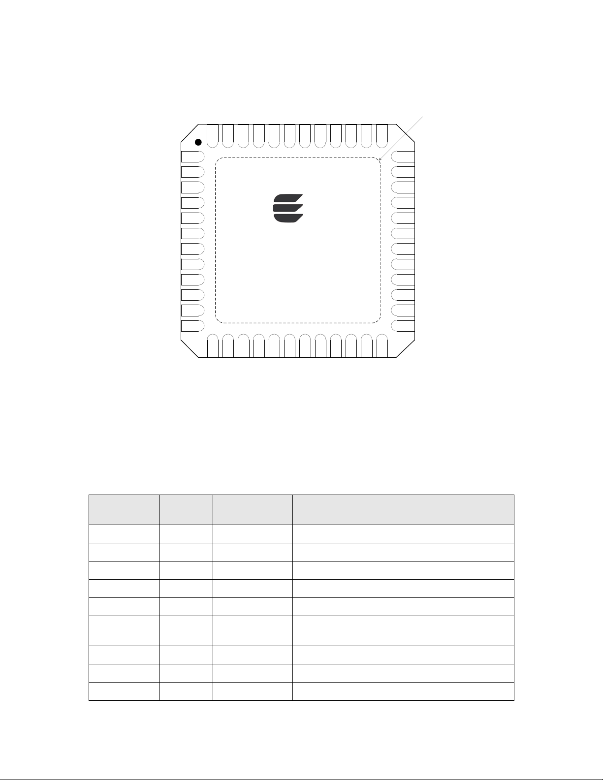
SVC~
IO0
IO1
IO2
IO3
VDD1V8
IO4
VDD3V3
IO5
IO6
IO7
IO8 VDDPLL
GNDPLL
VOUT1V8
RST~
VIN3V3
VDD3V3
AVDD3V3
CP0
AGND
CP1
NC
GND
IO9
IO10
IO11
VDD1V8
TRST~
VDD3V3
TCK
TMS
TDI
TDO
XIN
XOUT
CP2
CP3
CP4
CS0~
VDD3V3
VDD3V3
SDA_CS1~
VDD1V8
SCL
MISO
SCK
MOSI
37
38
39
40
41
42
43
44
45
46
47
48
1
2
3
4
5
6
7
8
9
10
11
12
13
14
15
16
17
18
19
20
21
22
23
24
25
26
27
28
29
30
31
32
33
34
35
36
Neuron 6000
Processor
®
GND PAD
VDD1V8
6
Power
1.8 V Power Input
VDD3V3
8
Power
3.3 V Power
Figure 9. Neuron 6000 Processor Pinout Diagram
Table 15 lists the pin assignments for the Neuron 6000 Processor. All digital inputs are low-
voltage transistor-transistor logic (LVTTL) compatible, 5 V tolerant, with low leakage. All
digital outputs are slew-rate limited to reduce Electromagnetic Interference (EMI) concerns.
Name
SVC~ 1 Digital I/O Service (active low)
IO0 2 Digital I/O IO0 for I/O Objects
IO1 3 Digital I/O IO1 for I/O Objects
IO2 4 Digital I/O IO2 for I/O Objects
IO3 5 Digital I/O IO3 for I/O Objects
IO4 7 Digital I/O IO4 for I/O Objects
IO5 9 Digital I/O IO5 for I/O Objects
Table 15. Neuron 6000 Processor Pin Assignments
Pin
Number Type Description
(from internal voltage regulator)
Series 6000 Chip Data Book 37
Page 50

IO6
10
Digital I/O
IO6 for I/O Objects
IO8
12
Digital I/O
IO8 for I/O Objects
IO10
14
Digital I/O
IO10 for I/O Objects
VIN3V3
29
Power
3.3 V Power Input
AVDD3V3
31
Power
3.3 V Power
AGND
33
Ground
Ground
Pin
Name
IO7 11 Digital I/O IO7 for I/O Objects
IO9 13 Digital I/O IO9 for I/O Objects
IO11 15 Digital I/O IO11 for I/O Objects
VDD1V8 16 Power 1.8 V Power Input
TRST~ 17 Digital Input JTAG Test Reset (active low)
VDD3V3 18 Power 3.3 V Power
TCK 19 Digital Input JTAG Test Clock
TMS 20 Digital Input JTAG Test Mode Select
TDI 21 Digital Input JTAG Test Data In
Number Type Description
(from internal voltage regulator)
TDO 22 Digital Output JTAG Test Data Out
XIN 23 Oscillator In Crystal oscillator input
XOUT 24 Oscillator Out Crystal oscillator output
VDDPLL 25 Power 1.8 V Power Input
(from internal voltage regulator)
GNDPLL 26 Power Ground
VOUT1V8 27 Power 1.8 V Power Output
(of internal voltage regulator)
RST~ 28 Digital I/O Reset (active low)
VDD3V3 30 Power 3.3 V Power
CP0 32 Comm Single-Ended Mode: Receive serial data
Special-Purpose Mode: Receive serial data
CP1 34 Comm Single-Ended Mode: Transmit serial data
Special-Purpose Mode: Transmit serial data
38 Hardware Resources
NC 35 N/A Do Not Connect
GND 36 Ground Ground
CP2 37 Comm Single-Ended Mode: External transceiver
enable
Special-Purpose Mode: Bit clock
Page 51

Pin
CP3
38
Comm
Do Not Connect
VDD3V3
42
Power
3.3 V Power
Name
Number Type Description
CP4 39 Comm Single-Ended Mode: Collision detect
Special-Purpose Mode: Frame clock
CS0~ 40 Digital I/O for
SPI slave select 0 (active low)
Memory
VDD3V3 41 Power 3.3 V Power
SDA_CS1~ 43 Digital I/O for
Memory
I2C: serial data
SPI: slave select 1 (active low)
VDD1V8 44 Power 1.8 V Power Input
(from internal voltage regulator)
SCL 45 Digital I/O for
I2C serial clock
Memory
MISO 46 Digital I/O for
SPI master input, slave output (MISO)
Memory
SCK 47 Digital I/O for
SPI serial clock
Memory
MOSI 48 Digital I/O for
SPI master output, slave input (MOSI)
Memory
PAD 49 Ground Pad Ground
Pin Connections
This section describes the electrical connections for the various pins on a Series 6000 chip.
Unless specified otherwise, the connections apply to both the FT 6000 Smart Transceiver and
the Neuron 6000 Processor.
See Appendix E, Example Schematic, for a more complete example schematic for an FT 6000
Smart Transceiver.
Connect the VDD3V3 pins (8, 18, 29, 30, 41, and 42) to V
pin (31) to an analog V
source, if different from the digital V
DD33
VDD3V3 pins and the AVDD3V3 pin connect to the same V
decoupling capacitors to the VDD3V3 pins, as shown in Figure 10.
Series 6000 Chip Data Book 39
. Also connect the AVDD3V3
DD33
source. In general, the
DD33
source. In addition, connect
DD33
Page 52
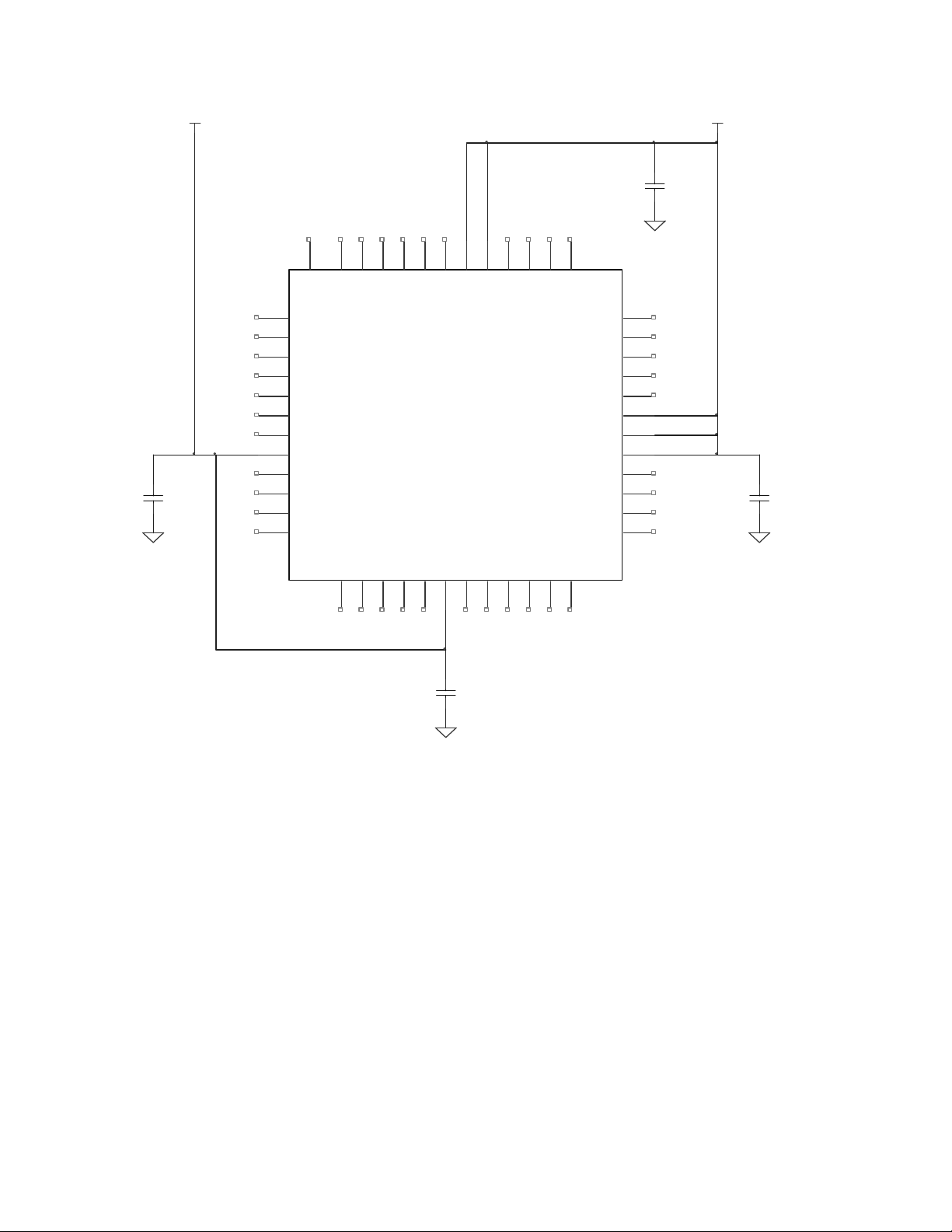
FT 6000
Smart Transceiver
U1
FT 5000
SVC~
1
IO0
2
IO1
3
IO2
4
IO3
5
VDD1V8
6
IO4
7
VDD3V3
8
IO5
9
IO6
10
IO7
11
IO8
12
IO9
13
IO10
14
IO11
15
VDD1V8
16
TRST~
17
VDD3V3
18
TCK
19
TMS
20
TDI
21
TDO
22
XIN
23
XOUT
24
VDDPLL
25
GNDPLL
26
VOUT1V8
27
RST~
28
VIN3V3
29
VDD3V3
30
AVDD3V3
31
NETN
32
AGND
33
NETP
34
NC
35
GND
36
TXON
37
RXON
38
CP4
39
CS0~
40
VDD3V3
41
VDD3V3
42
SDA_CS1~
43
VDD1V8
44
SCL
45
MISO
46
SCK
47
MOSI
48
GND
49
VDD33 VDD33
C2
0.1 uF
12
C1
0.1 uF
12
C4
0.1 uF
1
2
C3
0.1 uF
12
In the figure, the capacitors are:
• C1-C4: 0.1 µF Ceramic
The VOUT1V8 pin (27) is the output of the on-chip voltage regulator. Connect the VDD1V8
pins (6, 16, and 44) to the VOUT1V8 pin (27) to connect the 1.8 V input pins to the output of
the internal voltage regulator, as shown in Figure 11. Connect a bulk decoupling capacitor
(C5 in Figure 11) near the VOUT1V8 pin (27), in addition to the other decoupling capacitor.
Important: Do not connect an external 1.8 V source to any of the VDD1V8 pins (6, 16, and
44). Connect these pins to the VOUT1V8 pin (27) only. Using an external 1.8 V source
voids the warranty for the chip, and can cause unpredictable and possibly
irreparable results.
Figure 10. Connections for the VDD33 Pins
40 Hardware Resources
Page 53
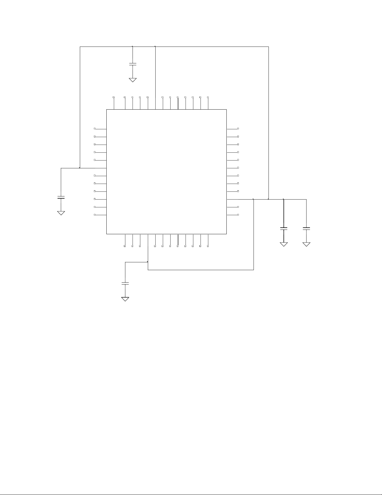
FT 6000
Smart Transceiver
U1
FT 5000
SVC~
1
IO0
2
IO1
3
IO2
4
IO3
5
VDD1V8
6
IO4
7
VDD3V3
8
IO5
9
IO6
10
IO7
11
IO8
12
IO9
13
IO10
14
IO11
15
VDD1V8
16
TRST~
17
VDD3V3
18
TCK
19
TMS
20
TDI
21
TDO
22
XIN
23
XOUT
24
VDDPLL
25
GNDPLL
26
VOUT1V8
27
RST~
28
VIN3V3
29
VDD3V3
30
AVDD3V3
31
NETN
32
AGND
33
NETP
34
NC
35
GND
36
TXON
37
RXON
38
CP4
39
CS0~
40
VDD3V3
41
VDD3V3
42
SDA_CS1~
43
VDD1V8
44
SCL
45
MISO
46
SCK
47
MOSI
48
GND
49
C4
0.1 uF
12
C5
1.0 uF
12
C1
0.1 uF
12
C3
0.1 uF
12
C2
0.1 uF
1
2
In the figure, the capacitors are:
Connect the chip’s pad (pin 49) to logic ground. Also connect the AGND pin (33) to logic
ground. Figure 12 shows the connections for the ground pins.
• C1-C4: 0.1 µF Ceramic
• C5: 1.0 µF Ceramic
Figure 11. Connections for the VDD18 Pins
Series 6000 Chip Data Book 41
Page 54
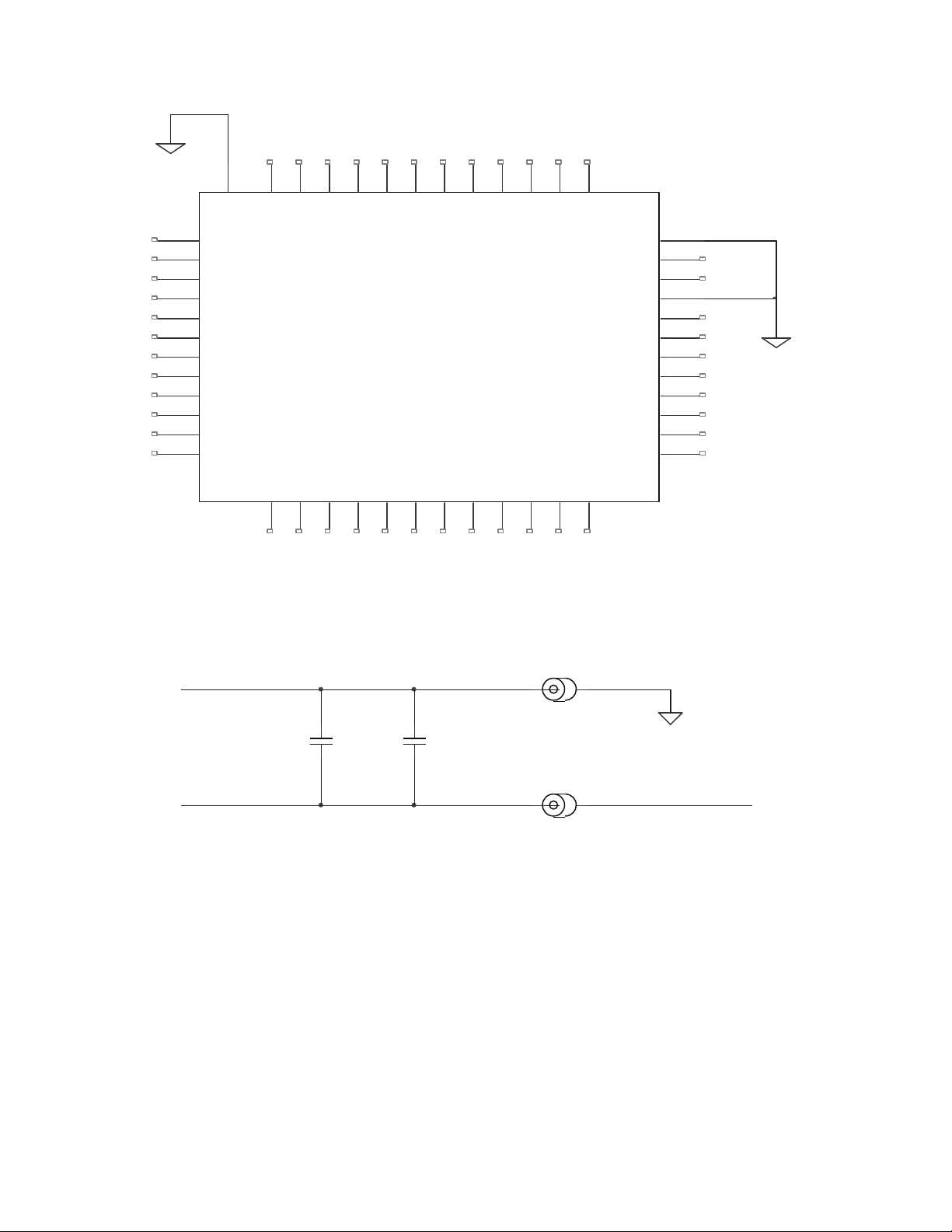
FT 6000
Smart Transceiver
U
1
FT 5000
SVC~
1
IO
0
2
IO1
3
IO2
4
IO
3
5
VDD1V8
6
IO4
7
VDD3V3
8
IO5
9
IO6
10
IO7
11
IO8
12
IO
9
13
IO10
14
IO11
15
VDD1V8
16
TRST~
17
VDD3V3
18
TCK
19
TMS
20
TDI
21
TDO
22
XIN
23
XOUT
24
VDDPLL
25
GNDPLL
26
VOUT1V8
27
RST~
28
VIN3V3
29
VDD3V3
30
AVDD
3V
3
31
NETN
32
AGND
33
NETP
34
NC
35
GND
36
TXON
37
RXON
38
CP4
39
CS0~
40
VDD3V3
41
VDD3V3
42
SDA_CS1~
43
VDD1V
8
44
SCL
45
MISO
46
SCK
47
MOSI
48
GND
49
C1
0.01 uF
12
C2
0.1 uF
12
L1
BEAD
1 2
L2
BEAD
1 2
GNDPLL
VDDPLL VOUT1V8
Figure 12. Connections for the Ground Pins
Connect the VDDPLL pin (25) to the VOUT1V8 pin (27), with an associated chip ferrite
bead, as shown in Figure 13. Connect the GNDPLL pin (26) to GND, with an associated
chip ferrite bead. In addition, add stabilizing capacitors across the VDDPLL and GNDPLL
pins. Place each capacitor directly adjacent to the PLL pins, on the top layer of the PCB.
In the figure, the capacitors are:
• C1: 0.01 µF Ceramic
• C2: 0.1 µF Ceramic
The chip ferrite beads should be rated for ≥50 mA saturation current, provide ≥120 Ω
impedance at 100 MHz per 20 ºC, and have a DC resistance ≤1 Ω. An example part is the
Laird Technologies
Connect a 1 to 10 kΩ pull-up resistor to the JTAG TCK pin (19), as shown in Figure 14.
®
Figure 13. Connections for the PLL Pins
LI0603E151R-10 part (formerly a Steward part).
42 Hardware Resources
Page 55

VDD3
R1
4.99k
12
TCK
Figure 14. Connection for the JTAG TCK Pin
Characteristi cs of the Digital Pins
Series 6000 chips provide 12 bidirectional I/O pins that are usable in several different
configurations. These pins provide flexible interfacing to external hardware and access to
the internal timer/counters. In addition to reading the input pins, the application processor
can read the current logic level of the output pins.
The digital I/O pins (IO0 – IO11) have LVTTL-level inputs. Pins IO0 – IO7 also have lowlevel-detect latches. The RST~ and SVC~ pins have internal pull-ups, and the RST~ pin
has hysteresis.
See the I/O Model Reference for Smart Transceivers and Neuron Chips for more information
about how to use the digital I/O pins.
Table 16 lists the characteristics of the digital I/O pins, which include the IO0 – IO11 pins,
the memory I/O pins, the Neuron 6000 CP0 – CP4 pins, and the other digital pins listed in
Table 14 and Table 15.
Table 16. Series 6000 Chip Digital Pin Characteristics
Parameter
VOH Output drive high at IOH = 8 mA 2.4 V — V
[1]
Description Minimum Typical Maximum
DD3
VOL Output drive low at IOL = 8 mA GND — 0.4 V
VIH Input high level 2.0 V — 5.5 V
VIL Input low level GND — 0.8 V
V
Input hysteresis for RST~ pin
HYS
— 300 mV —
and TCK pin
IIN Input leakage current — — 10 µA
RPU Pullup resistance
[2]
13 kΩ
—
23 kΩ
IPU Pullup current when pin at 0 V
[2]
130 µA — 275 µA
Series 6000 Chip Data Book 43
Page 56

Notes:
1. All parameters assume nominal supply voltage (V
between –40 ºC and +85 ºC), unless otherwise noted.
(T
A
2. Applies to RST~ and SVC~ pins only.
= 3.3 V) and operating temperature
DD3
Communications Port (CP) Pins for the Neuron 6000 Processor
The Neuron 6000 Processor has a very versatile communications port. It consists of five pins
(named CP0 through CP4) that can be configured to interface to a wide variety of media
interfaces (network transceivers) and operates over a wide range of data rates.
The communications port can be configured to operate in one of two modes: single-ended
mode or special-purpose mode. Table 17 lists the pin assignments for the communications
port pins for each of the modes, and Figure 15 shows a block diagram of the communications
port.
Table 17. Communications Port Pin Assignments
Special-Purpose
Drive
Pin
CP0 N/A Data input Rx input Transceiver RXD
Current
Single-Ended Mode
(3.3 V)
Mode
(3.3 V) Connect To
CP1 8 mA Data output Tx output Transceiver TXD
CP2 8 mA Transmit Enable
output
CP3 N/A Do Not Connect
CP4 8 mA Collision Detect input Frame Clock output Collision Detect
Before programming, a Neuron 6000 Processor uses its default communications parameters,
which define a simplified single-ended mode 78 kbps channel. The default communications
parameters allow you to load an application image over a 78 kbps network, for example
during device manufacturing. Devices that use a 78 kbps transceiver (such as a 78 kbps
EIA-485 transceiver or an LPT-11 Link Power Transceiver) can use the default
communications parameters within development or manufacturing test networks. For
production networks (networks with many devices), you should ensure that each device has
communications parameters defined for the channel; use the IzoT NodeBuilder Development
Tool to develop applications with the correct communications parameters. Note that devices
defined for a TP/XF-1250 channel cannot use the default communications parameters; each
Bit Clock output Transmit Enable
(single ended mode)
Bit Clock
(special-purpose mode)
(single ended mode)
Frame Clock
(special-purpose mode)
44 Hardware Resources
Page 57
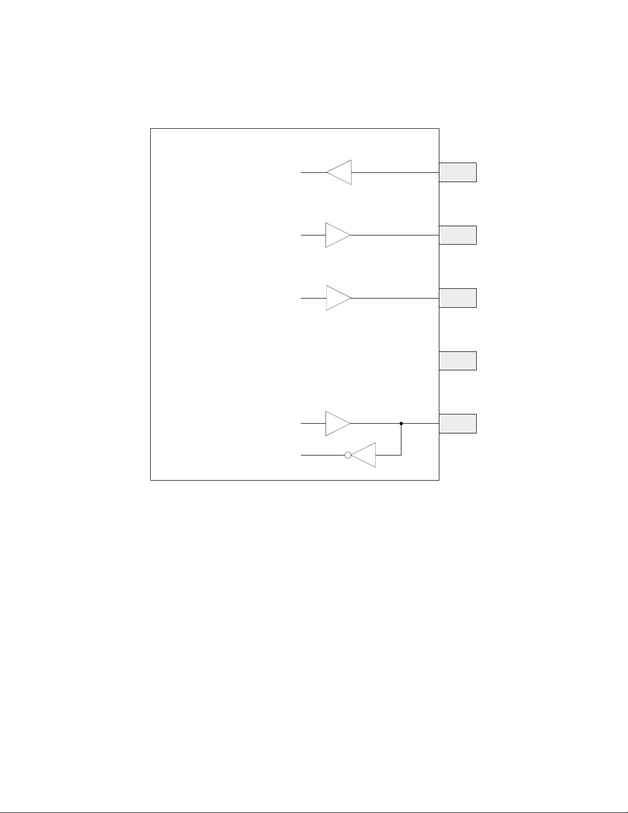
device’s external serial non-volatile memory must be loaded with the correct communications
CP
0
CP
1
CP2
CP3
CP4
Single-
Ended or Special-
Purpose RX (
in)
Single-
Ended or Special-
Purpose TX (
out
)
Single-
Ended TX Enable or
Special-
Purpose Bit Clock
(out)
Frame Clock (out)
Collision Detect (in)
Neuron
6000 Processor
parameters before connecting to the network.
Figure 15. Internal Transceiver Block Diagram
Single-ended mode uses Differential Manchester encoding (also known as bi-phase space
encoding), which is a widely used and reliable format for transmitting data over various
media. This encoding scheme provides a transition at the beginning of every bit period to
synchronize the receiver clock (referred to as the clock transition). The data is indicated by
the presence or absence of a second transition (the data transition) halfway between clock
transitions. A mid-cell transition indicates a zero. Lack of a mid-cell transition indicates a
one.
The transmitter transmits a preamble at the beginning of a packet to allow the other devices
to synchronize their receiver clocks. The preamble consists of a bit-sync field and a byte-sync
field. The bit-sync field is a series of Differential Manchester ones; its duration is user
selectable, and is at least four bits long. The byte-sync field is a single bit Differential
Manchester zero that marks the end of the preamble, and the beginning of the first data byte
of the packet.
The Neuron Chip terminates the packet by forcing a Differential Manchester code violation,
that is, the Neuron Chip holds the data output transitionless long enough for the receiver to
recognize an invalid code that signals the end of transmission. The data output can be either
high or low for the duration of the line-code violation, depending on the state of the data
Series 6000 Chip Data Book 45
Page 58

output after transmitting the last bit. The line-code violation begins after the end of the last
CRC bit, and lasts for at least 2.5 bit times. The last bit does not have a trailing clock edge.
The Transmit Enable pin is held active until the end of the line-code violation, and is then
released.
Differential Manchester coding is polarity-insensitive. Thus, reversal of polarity in the
communication link does not affect data reception.
A Neuron Chip in single-ended mode supports any of the following network bit rates:
• 2.5 Mbps
• 1.25 Mbps
• 625 kbps
• 312.5 kbps
• 156 kbps
The 625 kbps and lower bit rates are available for any of the system-clock rates of the
Neuron 6000 Processor. The 2.5 Mbps bit rate requires the Neuron 6000 Processor’s system
clock to be set at 40 MHz or higher, and the 1.25 Mbps bit rate requires the clock to be set to
20 MHz or higher.
• 78 kbps
• 39 kbps
• 19.5 kbps
• 9.6 kbps
• 4.8 kbps
Single-Ended Mode
Single-ended mode (3.3 V) is most commonly used with external active transceivers that
interface to media such as RF, IR, fiber optics, twisted-pair cable, and coaxial cable. Figure
16 shows the communications port configuration for single-ended mode operation. Data
communication occurs through the single-ended (with respect to GND) input and output
buffers on pins CP0 and CP1.
46 Hardware Resources
Page 59

CP
0
CP1
CP2
CP
3
CP4
TransmitEnable
Neuron
6000
Processor
Data Input
Data Output
Transmit Enable Output
CollisionDetect
~
Input
Differential Manchester
Decoder
Differential Manchester
Encoder
CollisionDetectEnable
NRZ
Data
NRZ
Data
Do Not Connect
CollisionDetect
Figure 16. Single-Ended Mode Configuration
Figure 17 shows a typical packet, where T is the bit period, equal to 1/(bit rate). Clock
transitions occur at the beginning of a bit period, and therefore, the last valid bit in the
packet does not have a trailing clock edge.
Figure 17. Single-Ended Mode Data Format
Before beginning to transmit the packet, the Neuron Chip initializes the output data pin to
start low. It then asserts the Transmit Enable pin (CP2) to ensure that the first transition in
the packet is from low to high. This first transition occurs within 1 bit time of asserting
Transmit Enable, and marks the beginning of the packet.
Series 6000 Chip Data Book 47
Page 60

Important: Transmit Enable is actively driven at all times in single-ended mode. In singleended mode, the 8 mA driver is connected to CP1 and it is not high impedance when
receiving packets.
At the end of the packet after the Differential Manchester code violation, the Transmit
Enable pin on CP2 is driven low to indicate the end of transmission.
Collision Detection for Single-Ended Mode
As an option, the Neuron Chip accepts an active-low Collision Detect input from the
transceiver. If collision detection is enabled, and CP4 goes low for at least one system clock
period (12.5 ns with an 80 MHz system clock) during transmission, the Neuron Chip is
signaled that a collision has occurred (or is occurring) and that the message must be sent
again. The device then attempts to re-access the channel.
The collision detect flag is checked by firmware at the end of the preamble and end of packet.
If the node does not use collision detection, the only way that it can determine that a
message has not been received is to request an acknowledgment. When acknowledged
service is used, the retry timer is set to allow sufficient time for a message to be sent and
acknowledged (typically 48 ms to 96 ms at 1.25 Mbps when there are no routers in the
transmission path). If the retry timer times out, the device attempts to re-access the
channel. The benefit of using collision detection is that the device does not have to wait for
the retry timer to time-out before attempting to resend the message, because the device
detects the collision when it sends the packet.
Beta 1 and Beta 2 Tim eslots in Single-Ended Mode
Important: The information in this section applies only to development of new network
types. If you use a standard L
work with the Beta 1 and Beta 2 timeslots.
The idle period between packets comprises the Beta 1 and Beta 2 timeslots. The Beta 1 time
is the fixed component in the idle period after a packet has been sent. This component is a
function of the following:
• Oscillator frequencies and accuracies on the various network devices.
• Media indeterminate time — that time following packet transmission when the
network can appear to be busy due to ringing on the line.
• Minimum interpacket gap — transceiver-dependent timing requirements.
• Receive-end delay — skew between the transmitter Neuron Chip’s and the receiver
Neuron Chip’s view of the end of the packet. This skew can occur because of
buffering in the transceivers, and is typically found in special-purpose mode
transceivers.
The Media Access Control (MAC) Layer timings are a function of five parameters stored in
the configuration data. These parameters determine the Preamble Length, the Packet Cycle,
the Beta 2 Slot Width, the Transmit Interpacket Padding, and the Receive Interpacket
Padding.
ONMARK channel in a LONWORKS network, you do not need to
All timings are given in terms of the Neuron Chip processor cycles. One cycle is 37.5 ns at 80
MHz, 75 ns at 40 MHz, 150 ns at 20 MHz, 0.3 μs at 10 MHz, and 0.6 μs at 5 MHz:
48 Hardware Resources
Page 61

• Beta 1 Time after Transmission = 583 cycles + Transmit Interpacket Padding + Beta
2 Slot Width
• Beta 1 Time after Reception = 565 cycles + Receive Interpacket Padding + Beta 2 Slot
Width
An indeterminate time is defined during the Beta 1 period in which all transitions on the
channel are ignored. This period starts following the end of any packet (transmitted or
received). Its duration is defined as follows:
• Indeterminate Time after transmission = 313 cycles + Transmit Interpacket Padding
• Indeterminate Time after reception = 295 cycles + Receive Interpacket Padding
Both priority (P) and non-priority slots are defined by the Beta 2 time. Devices listen to the
network prior to transmitting a packet. This prevents devices from transmitting packets on
top of each other except when the packets are initiated at nearly the same time. In addition,
devices randomize the time before they start transmitting on the network. When the
network is idle, all nodes randomize over 16 slots. As the estimated network load increases,
devices start randomizing over more slots to lower the probability of a collision. The number
of randomizing slots (R) varies from 16 up to 1008, based on “n,” the estimated channel
backlog (the number of slots is n•16 where “n” has a range of 1 to 63), as shown in Figure
18.
Figure 18. Packet Timing
Following a packet, and prior to randomizing, devices wait for a configurable number of
priority slots to pass. Devices with priority packets and a configured priority slot transmit in
a priority slot. Use of priority substantially reduces the probability of collision. The number
of priority slots (P) is fixed for a given channel and can range from 0 to 127.
The Beta 2 time is defined by the following:
• Oscillator frequencies and accuracies on the various network devices.
• Number of priority slots on the channel.
• Receive start delay — the time from when a device starts transmitting to when the
receiving device detect the start of transmission. This delay is a function of the
receive-to-transmit turnaround time of the transceiver, the bit rate and length of the
media, delay through the receiver, and initial preamble bits lost.
• For special-purpose mode transceivers, framing delays between the Neuron Chip and
the transceiver.
For the receiver to detect the edge transitions, two windows are set up for each bit period, T.
The first window is set at T/2 and determines if a zero is being received. The second window
is at T and defines a one. This transition then sets up the next two windows (T/2 and T). If
no transition occurs, a Differential Manchester code violation is detected and the packet is
assumed to have ended.
Table 18 shows the width of this window. If a transition falls outside of either window, it is
not detected. Timing instability of the transitions, known as jitter, can be caused by changes
Series 6000 Chip Data Book 49
Page 62

PATENT NOTICE
in the communications medium, or instability in the transmitting or receiving device’s input
clocks. The jitter tolerance windows are expressed as fractions of the bit period, T.
Table 18. Receiver Jitter Tolerance Windows
Next Clock Edge
Next Data Edge (Nominal)
0.500T 1.000T 1.46T
For the receiver to reliably terminate reception of a packet, the received line-code violation
period must have no transitions until the Neuron Chip detects the end of the packet. The
receiving Neuron Chip terminates a packet if no clock transitions are detected after the last
bit. Table 18 shows the minimum duration from the last clock edge to where the Neuron
Chip is guaranteed to recognize the line-code violation. Data transitions are allowed in this
period (and must fall within the data window).
For a Neuron Chip, the time from when an application software call is issued to send a 12byte message to when the packet is sent is approximately 175 µs for an 80 MHz system clock
(the time varies inversely with the system clock rate).
(Nominal)
Line Code Violation to
Receive (Minimum)
Special-Purpos e M ode
In special situations, it is desirable for the Neuron Chip to provide the packet data in an
unencoded format and without a preamble. In this case, an intelligent transmitter accepts
the unencoded data and does its own formatting and preamble insertion. The intelligent
receiver then detects and strips off the preamble and formatting, and returns the decoded
data to the Neuron Chip.
The Special-Purpose Mode is protected by U.S. Patent No. 5,182,746 and foreign patents
based on this patent. No express or implied license is granted herein with respect to such
patents. If you are interested in obtaining a non-exclusive, royalty free license to these
patents, please call Echelon at +1 (408) 938 5200 and ask for Contracts Management.
Such an intelligent transceiver contains its own input and output data buffers and intelligent
control functions, and provides handshaking signals to properly pass the data back and forth
between the Neuron Chip and the transceiver. In addition, there are many features that can
be defined by and incorporated into a special-purpose transceiver:
• Ability to configure various parameters of the transceiver from the Neuron Chip
• Ability to report on various parameters of the transceiver to the Neuron Chip
• Multiple channel operation
• Multiple bit rate operation
• Use of forward error correction
• Media-specific modulation techniques requiring special message headers and framing
• Collision detection
While the special-purpose mode offers custom features, it is expected that most transceivers
will use the single-ended mode for most types of media. This is because single-ended mode
offers Differential Manchester encoding, which takes care of clock recovery, whereas specialpurpose mode does not have this feature. In addition, the special-purpose mode is a
50 Hardware Resources
Page 63

restricted protocol that Echelon licenses for use only when the Neuron Chip and transceiver
are sold as one unit. For more details, contact Echelon Support.
When the special-purpose mode (3.3 V) is used, the Neuron 6000 Processor and the
transceiver use a protocol that consists of the Neuron 6000 Processor and the transceiver
each exchanging 16 bits (8 bits of status and 8 bits of data; see Figure 19) simultaneously
and continuously at rates up to 20.0 Mbps (when the Neuron Chip’s system clock is 80 MHz).
The 20.0-Mbps bit rate allows time-critical flags, such as a Carrier Detect, to be exchanged
across the interface with network bit rates up to 625 kbps. The maximum bit rate is 625
kbps because of the overhead associated with the handshaking.
Figure 19. Special-Purpose Mode Data Format
The Neuron Chip communicates with the transceiver through its CP[4:0] pins. CP4 and CP2
are synchronizing clocks generated by the Neuron Chip: CP4 is a frame clock, and CP2 is a
bit clock. CP0 and CP1 contain the exchanged data: CP0 transfers data from the transceiver
to the Neuron Chip, and CP1 transfers data from the Neuron Chip to the transceiver.
The Neuron Chip and transceiver continuously exchange data through its CP0 and CP1 pins.
The bit clock defines transitions between bits in the data stream. The Neuron Chip uses the
falling edge of the bit clock to both sample CP0 and change CP1 to the next bit. The
transceiver should use the rising edge of bit clock to sample CP1 and update CP0.
The serial data streams on CP0 and CP1 are divided into 16-bit frames. The frame clock
(CP4) is used to define the boundaries of the frames. The frame clock is active (high) while
the Neuron Chip is outputting the least-significant bit (LSB) of the frame on CP1. On the
falling edge of the frame clock, the Neuron Chip is sampling the most-significant bit (MSB) of
the next frame on CP0.
The first eight bits of each frame are interpreted as the status field and the last eight bits as
the data field. The status field controls transceiver operation and controls passing data
between the Neuron Chip and the transceiver. The interpretation of each status bit is shown
in Table 19 and Table 20.
Series 6000 Chip Data Book 51
Page 64

Table 19. Special-Purpose Mode Transmit Status Bits
Bit Flag Description
7 TX_FLAG Neuron Chip in the process of transmitting packet
6 TX_REQ_FLAG Neuron Chip requests to transmit on the network
5 TX_DATA_VALID Neuron Chip is passing network data to the transceiver in
this frame
4 Don’t Care Unused
3 TX_ADDR_R/W If negated, Neuron Chip is writing internal transceiver
register
2 TX_ADDR_2 Address bit 2 of internal transceiver register [1..7]
1 TX_ADDR_1 Address bit 1 of internal transceiver register [1..7]
0 TX_ADDR_0 Address bit 0 of internal transceiver register [1..7]
Note: For bits [2..0] the internal transceiver register 0 is not valid. Registers [1..7] are
defined by the transceiver implementation.
Table 20. Special-Purpose Mode Receive Status Bits
Bit Flag Description
7 SET_TX_FLAG Transceiver accepts request to transmit packet
6 CLR_TX_REQ_FLAG Transceiver acknowledges request to transmit packet
5 RX_DATA_VALID Transceiver is passing network data to the Neuron Chip
in this frame
4 TX_DATA_CTS Transceiver indicates that Neuron Chip is clear to send
byte of network data
3 SET_COLL_DET Transceiver has detected a collision while transmitting
the preamble
2 RX_FLAG Transceiver has detected a packet on the network
1 RD/WR_ACK Transceiver acknowledges read/write to internal register
0 TX_ON Transceiver is transmitting on the network
There are three types of data that can be sent and received during each frame:
1. Network packet data — Actual data (8 bits at a time) that is to be transmitted or has
been received.
52 Hardware Resources
Page 65

2. Configuration data — Information from the Neuron Chip that tells the transceiver
how it is to be set up or configured.
3. Status data — Informational parameters reported from the transceiver to the Neuron
Chip (when requested by the Neuron Chip).
The contents of the configuration data and status data are defined by the transceiver.
The Neuron Chip controls the communication with the transceiver by asserting and
examining status bits. There are four basic operations that the Neuron Chip performs with
the transceiver: transmit packet, receive packet, write configuration, and read status.
When the Neuron Chip wants to transmit a packet, it sets the TX REQ FLAG bit of its
output status field. The transceiver can then accept or reject the request. To reject the
request, the transceiver sets the CLR TX REQ FLAG bit and clears the SET TX FLAG bit.
The transceiver indicates that it is ready to transmit by setting the CLR TX REQ FLAG and
SET TX FLAG bits for one frame. In that same frame, the transceiver must also set the TX
DATA CTS bit to indicate that the Neuron Chip can send the first byte of data.
The Neuron Chip sends a packet of data only if the transceiver accepts the transmit request.
The Neuron Chip then sets the TX FLAG bit for the entire duration of the packet. The
transceiver must set the TX ON bit while it is transmitting a packet.
Each byte is transferred from the Neuron Chip to the transceiver with a handshake protocol.
The transceiver indicates that it is ready to accept a byte by setting the TX DATA CTS bit for
a single frame. The Neuron Chip uses this flag to cause it to send out another byte in a
subsequent frame; the Neuron Chip also sets the TX DATA VALID bit during the frame that
contains the data byte.
After the Neuron Chip sends the last byte in the packet, it clears the TX FLAG bit to indicate
the end of transmission. When the transceiver finishes transmitting the packet, including
any error codes, it must clear the TX ON bit to indicate that it has released the network.
The transceiver can abort transmission if it detects a collision by setting the SET COLL DET
bit for one frame. The Neuron Chip then clears the TX FLAG bit and prepares to resend the
packet.
The transceiver initiates packet reception by setting the RX FLAG bit. The transceiver can
begin sending data to the Neuron Chip in the frame after setting the RX FLAG bit. Each
frame that contains valid data must be marked with the RX DATA VALID bit set. When the
transceiver finishes receiving a packet, it clears the RX FLAG bit and the Neuron Chip
terminates reception of the packet.
The Neuron Chip performs a configuration write or status read by using the TX ADDR R/W
and TX ADDR [2:0] bits. The TX ADDR [2:0] bits indicate which of seven transceiver
registers is being accessed, and the TX ADDR R/W bit indicates whether the operation is a
configuration register write (0) or status register read (1). Register 0 (TX ADDR [2:0] = 000)
is unused, so that TX ADDR R/W = 0 and TX ADDR [2:0] = 000 indicates no read or write
operation is to be performed.
To write to a configuration register, the Neuron Chip clears the TX ADDR R/W bit and
indicates the selected register with the TX ADDR [2:0] bits. The transceiver must
acknowledge that the operation is complete by setting the RD/WR ACK bit. The Neuron
Chip continues to send the configuration write command until it receives a frame with the
RD/WR ACK bit set.
To read a status register, the Neuron Chip sets the TX ADDR R/W bit and indicates the
selected register with the TX ADDR [2:0] bits. The transceiver must acknowledge that the
operation is complete by setting the RD/WR ACK bit and by placing the requested
Series 6000 Chip Data Book 53
Page 66

D5
C3
C6
NETP
NETN
CP4
RXON
TXON
NETB
NETANETP
NETN
CTS2
CTS1
CTP2
CTP1
C4
Optional RXACTIVE
and TXACTIVE LEDs
D3
D6
D4
C
5
NET1
NET2
1
6
5
2
4
7
3
8
34
32
39
38
37
+
+
VR
1
FT
6000 Smart
Transceiver
FT-
X3
Communications
Transformer
+
3.3
V
R
1
C1
C2
D1B
D
2B
D
1A
D
2A
+
3
.
3
V
information in the data field. The Neuron Chip continues to send the status request
command until it receives a frame with the RD/WR ACK bit set.
Network Connection
How you connect a Series 6000 device to a network depends primarily on whether the Series
6000 device contains an FT 6000 Smart Transceiver or a Neuron 6000 Processor. For FT
6000 Smart Transceivers, you use the FT-X3 transformer; for Neuron 6000 Processors, you
use an external transceiver and associated interconnect circuitry.
Connection for an FT 6000 Smart Transceiver
Figure 20 shows the preferred interconnection between the FT 6000 Smart Transceiver and
the FT-X3 Communications Transformer; the figure also shows the associated transient
protection circuitry. Connect pins 1 and 6 of the FT-X3 transformer to the FT 6000 Smart
Transceiver, as shown in the figure. The figure is not a complete schematic, because it does
not include the clock, reset, and power supply bypass circuits for the FT 6000 Smart
Transceiver. See Appendix C, FT-X3 Communications Transformer, for a schematic view of
the FT-X3 Communications Transformer.
Figure 20. FT 6000 Smart Transceiver and FT-X3 Interconnections
Name Value Description
R1
VR1 470 V MOV, 5 mm, 40 pF
Table 21. External Components for FT 6000 Smart Transceiver
4.99 kΩ
(typical)
Pullup resistor
Panasonic ERZV05D471, Digi-Key
P7186-ND or equivalent
54 Hardware Resources
Page 67

Name Value Description
C1, C2 56 pF, 50 V Common-mode noise immunity
capacitors (for EN61000-4-6 Level 3)
C3, C4 100 pF, 5% Optional center-tap capacitors
C5, C6
D1, D2 BAV99 ESD transient clamping diodes
D3, D4, D5, D6
In Figure 20, diodes D1 and D2 are ESD transient clamping diodes. Capacitors C1 and C2
provide common-mode noise immunity for compliance with EN61000-4-6 Level 3. Capacitors
C5 and C6 are used to provide DC voltage isolation for the FT 6000 Smart Transceiver when
it is used on a link power network and to protect it in the event of a DC power fault on the
network wires. The capacitors are required to meet L
the TP/FT-10 channel. These capacitors are not needed for devices that will be connected
exclusively to non-link power networks and do not require protection against DC faults. Two
polar capacitors are used to protect against the application of a DC voltage of either polarity,
while providing a total capacitance of 11 μF. Alternatively, a single non-polar capacitor of 10
μF can be used in either of the two legs that connect to the network. The initial tolerance of
the capacitor should be ±20% or less, and degradation due to aging and temperature effects
should not exceed 20% of the initial minimum value.
In some cases, adding capacitors (C3 and C4) between the center tap pins and earth ground
can reduce EMI emissions.
22 μF, ≥50 V, polar
BAV99, 1N4148-equivalent
1N4934, 1N4935, FR1D,
RS1D, RS1DB
DC blocking capacitors
Differential network clamping diodes:
For up to 2 kV Surge Protection
For up to 6 kV Surge Protection
ONMARK interoperability guidelines for
Note that Series 3100 FT Smart Transceivers had a single COMM_ACTIVE pin (equivalent
to the CP2 pin for a Series 3100 Neuron Chip) that you could connect to a special
COMM_ACTIVE LED circuit to drive a pair of LEDs to display network activity. FT 6000
Smart Transceivers have two communications pins, TXON and RXON, that you can connect
to network activity LEDs (RXACTIVE and TXACTIVE) without any special circuitry
requirements. However, you might want to add pulse-stretching circuitry for these packetactivity signals for increased visibility. If your device does not require network activity
LEDs, pins 37 and 38 should be treated as No Connect.
Comparison with FT 3120 or FT 3150 Devices
The interconnection with the network transformer for an FT 3120 Smart Transceiver or an
FT 3150 Smart Transceiver is similar to the interconnection for an FT 6000 Smart
Transceiver (as described in Connection for an FT 6000 Smart Transceiver). However, FT
3120 and FT 3150 Smart Transceivers can use one of three transformers: the FT-X1 (a
through-hole part), the FT-X2 (a surface-mount part), or the FT-X3 (a surface-mount part).
Although you can use an FT-X1 or FT-X2 transformer with an FT 6000 Smart Transceiver,
you cannot simply replace an existing FT 3120 or FT 3150 Smart Transceiver with an FT
6000 Smart Transceiver. The voltage requirement is different (the FT 6000 Smart
Series 6000 Chip Data Book 55
Page 68

Transceiver is a 3.3 V part and the FT 3120 or FT 3150 Smart Transceiver is a 5 V part); the
packages are different; and the pinouts are different. In addition, if your Series 3100 device
uses a COMM_ACTIVE circuit to drive network-activity LEDs, the requirements for that
circuit are very specific for FT 3120 or FT 3150 Smart Transceivers, whereas for FT 6000
Smart Transceivers, you can use a simple LED driver circuit for the two network activity
LEDs.
See the FT 3120 / FT 3150 Smart Transceiver Data Book for more information about the
interface for FT 3120 or FT 3150 Smart Transceivers.
Comparison with Series 5000 Devices
For details of new features of the Series 6000 parts, please see What’s New for Echelon’s
Smart Transceivers and Neuron Chips
The pinout and packaging of both Series 5000 and Series 6000 parts are identical, thus
enabling a simple transition.
Comparison with the FTT-10A Transceiver
The FTT-10A transceiver is designed to be used with Neuron Chips (Series 3100, Series
5000, and Series 6000). The migration path from a Series 3100 Neuron Chip to a Series 3100
Smart Transceiver is fairly straightforward:
• The Series 3100 Smart Transceiver has the same footprint as the corresponding
Series 3100 Neuron Chip
• The FT-X1 transformer has the same footprint as the FTT-10A transceiver
• The pinout of the FT-X1 transformer is compatible with the connections between the
Series 3100 Neuron Chip and the FTT-10A transformer
See the FT 3120 and FT 3150 Smart Transceiver datasheet for more detailed information on
these pinouts and footprints.
A device based on a Series 3100 Smart Transceiver with the FT-X1 or FT-X2 transformer can
run the same applications with the same functionality as a 3100 Neuron Chip with an FTT10A transceiver. In addition, Series 3100 Smart Transceiver with the FT-X1, FT-X2, or FTX3 transformer has the same levels of transient immunity, but has improved magnetic field
noise immunity, and improved common-mode network noise immunity (as tested per EN
61000-4-6). See the FT 3120 / FT 3150 Smart Transceiver Data Book for more information
migrating from a 3100 Neuron Chip with an FTT-10A transceiver to a Series 3100 Smart
Transceiver with the FT-X1 or FT-X2 transformer.
The migration path from a Series 3100 Neuron Chip to a Series 6000 Smart Transceiver
requires additional design work:
• The Series 6000 Smart Transceiver is a 3.3 V part and the Series 3100 Neuron Chip
is a 5 V part
• The Series 6000 Smart Transceiver has a different footprint compared to the
corresponding Series 3100 Neuron Chip
• The FT-X3 transformer has a different footprint compared to the FTT-10A
transceiver
• The pinout of the FT-X3 transformer is not entirely compatible with the connections
between the Series 3100 Neuron Chip and the FTT-10A transformer
56 Hardware Resources
Page 69

A device based on a Series 6000 Smart Transceiver with the FT-X3 transformer can run the
same applications (after they are recompiled for the FT 6000 Smart Transceiver) with the
same functionality as a 3100 Neuron Chip with an FTT-10A transceiver or a Series 3100
Smart Transceiver with a FT-X1 or FT-X2 transformer. In addition, a Series 6000 Smart
Transceiver with the FT-X3 transformer has the same levels of transient immunity,
magnetic field noise immunity, and common-mode network noise immunity (as tested per EN
61000-4-6) as a Series 3100 device.
Connection for a Neuron 6000 Processor
You can connect a Neuron 6000 Processor to an external transceiver to communicate with a
TP/XF-1250 channel, an EIA-485 network, a link-power TP/FT-10 channel, or other
transceivers. Use an FT 6000 Smart Transceiver for a standard (non-link-powered) TP/FT10 channel or for a locally powered device on a link-power TP/FT-10 channel.
TPT/XF-1250 Transcei ver s
You can use the Neuron 6000 Processor with an Echelon TPT Twisted Pair Transceiver
Module for a TP/XF-1250 channel type. However, because the Neuron 6000 Processor does
not include an on-chip differential transceiver (that is, the Neuron 6000 Processor does not
support the differential mode of operation that Neuron 3120 Chips and Neuron 3150 Chips
supported), you must:
• Select “TP/XF-1250” as the transceiver type within the Hardware Template Editor of
the IzoT NodeBuilder Development Tool. This selection causes the Neuron firmware
to configure the Neuron 6000 Processor’s communications port to operate in 3.3 V
single-ended mode.
• Add a single-ended mode to differential mode converter circuit, as described in the
Connecting a Neuron 5000 Processor to an External Transceiver Engineering Bulletin
(005-0202-01B). This circuit converts the Neuron 5000 or Neuron 6000 Processor’s
3.3 V single-ended mode signals to the 5 V differential mode signals required for the
TPT/XF-1250 transceiver.
Figure 21 shows the basic configuration for connecting a Neuron 6000 Processor to a
TPT/XF-1250 transceiver.
Series 6000 Chip Data Book 57
Page 70

CP2
CP1
CP4
CP3
CP0
DATA_B
DATA_A
CP3
CP2
GND
VDD5
CP0
CP1
2
5
4
3
9
7
6
1
37 TXEN
34 TX
39
38
32 RX
Neuron 6000 Processor TPT/XF-1250
3.3 V Single-Ended Mode
+5 V
VDD3V3
+3.3 V
8
8
CT
NET1
NET2
+3.3 V
Differential Driver
Circuit
Comparator
Circuit
10k
+3.3 V
0.1 µF
+5 V
Figure 21. Connecting a Neuron 6000 Processor to a TP/XF-1250 Transceiver
In the figure, the pullup resistor for the Neuron Chip’s CP4 pin is optional, but helps prevent
contention on the CP4 pin if the Neuron Processor is incorrectly configured to operate in
special-purpose mode (for which the CP4 pin is an output). The diode clamps for the
TPT/XF-1250 transceiver’s CP0 and CP1 signals are high-speed switching diodes, such as
®
Fairchild Semiconductor
1N4148 small-signal diodes. The value of the capacitor on the
TPT/XF-1250 transceiver’s transformer center tap (CT) pin depends on the device’s PCB
layout and EMI characteristics. A typical value is 100 pF rated for 1000 V. For more
information about the TPT/XF-1250 transceiver, see the L
Transceiver Module User’s Guide (078-0025-01C).
The details of the required differential driver circuit and the comparator circuit for the
Neuron 5000 or Neuron 6000 are described in the Connecting a Neuron 5000 Processor to an
External Transceiver Engineering Bulletin (005-0202-01B).
EIA-485 Transceivers
You can use the Neuron 6000 Processor with commercially available EIA-485 transceivers.
Multiple data rates (up to 1.25 Mbps), and a number of wire types can be supported. With an
EIA-485 transceiver, common-mode voltage ranges between –7 V to +12 V. To implement an
EIA-485 device, the Neuron 6000 Processor’s communications port runs in single-ended
mode.
Available industry standards that describe EIA-485 specifications provide details on unit
loads, data rate, wire size, and wire distances. To ensure interoperability between devices,
ONMARK interoperability guidelines require a data rate of 39 kbps for devices that use
the L
EIA-485 transceivers. In addition, the EIA-485 transceiver must have TTL-compatible
ONWORKS TPT Twisted Pair
58 Hardware Resources
Page 71
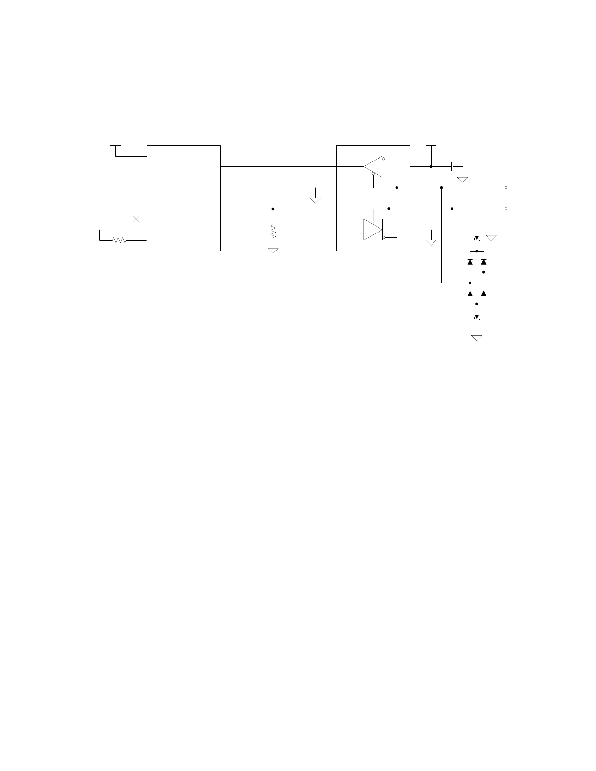
inputs for the connection to the Neuron 6000 Processor. A typical circuit configuration,
CP0
CP1
CP3
CP2
CP4
R
RE~
DE
D
A
B
VDD
GND
32 RX
34 TX
38
37 TXEN
39
Neuron 6000 Processor EIA-485 Transceiver
3.3 V Single
-Ended Mode
+5 V
VDD3V3
+3
.
3 V
8
0
.1
µF
10k
12V
12
V
MUR115
(x4)
A
B
10k
+
3
.3
V
shown in Figure 22, can support up to 32 loads.
Individual device power sources can create problems when the common voltage exceeds –7 V,
+ 12 V, or with ground faults.
Figure 22. EIA-485 Twisted-Pair Interface (Uses Single-Ended Mode)
The EIA-485 specification requires a common ground reference for all transceivers. This
common ground reference can be provided by adding a third conductor in the network cable
or a separate connection to common ground at each device.
LPT-11 Link Power Tran sceivers
The Echelon LONWORKS LPT-11 Link Power Twisted Pair Transceiver provides a simple,
cost effective method for adding a network-powered L
Chip-based sensor, activator, display, lighting device, or general purpose I/O controller. The
LPT-11 transceiver eliminates the need to use a local power supply for each device, because
device power is supplied by a central power supply over the same twisted wire pair that
handles network communications.
Figure 23 shows the basic configuration for connecting a Neuron 6000 Processor to an LPT11 Twisted-Pair Link Power Transceiver.
ONWORKS transceiver to any Neuron
Series 6000 Chip Data Book 59
Page 72
CP0
CP1CP3
CP2CP4
32 RX
34 TX38
37 TXEN39
Neuron 6000 Processor
LPT-11 Link Power
Transceiver
3.3 V SingleEnded Mode
8
NETB
NETA
R1
10k
+3.3 V
+5 V
RXD
TXD
GND
VCC
INDUCTOR
6
9
10
4
5
NET_A
NET_B
2
1
GND
36
VDD3V3
Low drop-out
linear regulator
L1
1 mH
+5 V+3.3 V
C4
0.1 pF
C3
22 µF
V+
3
C5
100 µF
OE
10 MHz
18 pF
C2
27 pF
C1
30 pF
R3
200
R2
1M
XOUTXIN
CLK
7
+5 V
23 24
GROUND GUARD
U1
U2
U3
R4
10k
Figure 23. Connecting a Neuron 6000 Processor to an LPT-11 Link Power Transceiver
The major differences between connecting a Series 3100 Neuron Chip to an LPT-11
transceiver (see the L
and connecting a Neuron 6000 Processor to an LPT-11 transceiver are:
• The connection between the LPT-11 VCC pin and the Neuron 6000 VDD3V3 pin
ONWORKS LPT-11 Link Power Transceiver User’s Guide, 078-0198-01A)
requires the addition of a low drop-out linear regulator to convert the +5 V output
from the LPT-11 transceiver to the +3.3 V input for the Neuron 6000 Processor.
• The connection between the LPT-11 TXD pin and the Neuron 6000 CP1 pin requires
the addition of a non-inverting bus buffer/line driver that supports TTL-compatible
input and 5V CMOS output. The output of the Neuron CP2 pin is also connected to
the buffer/line driver to allow the Neuron 6000 Processor to propagate a device reset
to the LPT-11 transceiver by setting the buffer/line driver to a tri-state impedance
See the Connecting a Neuron 5000 Processor to an External Transceiver Engineering Bulletin
(005-0202-01B) for additional information.
60 Hardware Resources
state. An example part for the buffer/line driver is an NXP
buffer/line driver.
• The connection between the LPT-11 CLK pin and the Neuron 6000 XOUT pin
requires the addition of a standard (inverting or non-inverting) bus buffer/line driver
that supports TTL-compatible input and 5V CMOS output.
®
74AHCT1G126 bus
Page 73
Clock Requirements
Y1
10.0000MHZ
200PPM
18pF
1
2
C2
30 pF
1
2
C1
30 pF
1
2
R1
1M
1
2
XIN XOUT
R2
200
1 2
A Series 6000 chip requires a 10 MHz external crystal or oscillator to provide its input clock
signal. The chip then multiplies the input frequency by an amount specified in the device’s
hardware template (specified during device development using the IzoT NodeBuilder
Development Tool) to derive its internal system clock frequency. For multipliers greater
than one, the chip uses a phase-locked loop (PLL) to drive and manage the internal on-chip
system clock frequency.
This section describes the requirements for the external crystal and compares terminology
for Series 6000 chip clock frequencies with Series 3100 chip clock frequencies.
External Crystal
A Series 6000 chip requires a 10.0 MHz external clock signal for operation. An example part
that meets the requirements for a Series 6000 chip is the Abracon Corporation
ABMM2100000MHzD1 Ceramic Surface Mount Low Profile Quartz Crystal.
The crystal must have a load capacitance rating of 18 pF. Because a Series 6000 chip does
not have internal load capacitance on-chip, you must add 30 pF combined external series
capacitance, as shown in Figure 24.
Unlike the Series 3100 chip, the Series 6000 chip’s XOUT pin cannot be used to drive an
external CMOS load. However, if you maintain the required capacitance for the XOUT pin,
you can drive an external clock, for example, as shown for the LPT-11 Link-Power
Transceiver in Figure 23.
module (such as a Vishay
If your device requires a common clock signal, you can use an external 3.3 V oscillator
XOUT unconnected. You could also define an output frequency I/O model for one of the
Series 6000 chip’s I/O pins (IO0..IO11) and connect the load’s clock signal to the Series 6000
chip’s I/O pin.
A 60/40 duty cycle or better is required for the external oscillator, as shown in Figure 25.
An external oscillator must provide low-voltage transistor-transistor logic (LVTTL) voltage
levels (0 to 3.3 V) to the XIN pin.
Series 6000 Chip Data Book 61
Figure 24. Series 6000 Chip Clock Generator Circuit
®
Intertechnology XOSM-533 Surface Mount Oscillator), and leave
Page 74

Figure 25. Test Point Levels for XIN Duty-Cycle Measurements
To ensure proper oscillator startup, the equivalent series resistance specification for the
crystal should be ≤50 Ω, and the crystal shunt capacitance should be no greater than 7 pF.
A Series 6000 chip requires a clock frequency with a total accuracy of ±200 ppm over the full
range of component tolerances and operating conditions, including oscillator tolerance,
crystal tolerance, PCB and capacitor variation, and aging. Variation within the Series 6000
chip uses a portion of the overall ±200 ppm budget. Its duty cycle symmetry must be no
worse than 60/40%. In addition, the voltage swing of the clock signal must be within the
GND and V
an appropriate parallel resonant crystal to the XIN and XOUT pins of the Series 6000 chip,
as shown in Figure 24.
The remaining portion of the error budget allocated for total crystal uncertainty is ±85 ppm
(assuming that the selected crystal has a load capacitance specification that matches the
circuit loading). Total crystal uncertainty is the combination of the crystal’s initial frequency
tolerance plus its temperature and aging tolerances. Note that a typical crystal aging
specification is 5 ppm/yr but, because the aging effect tends to follow a logarithmic curve,
aging over a 10 year span is commonly in the range of 10 to 15 ppm (contact individual
crystal vendors for detailed specifications).
supply rails of the Series 6000 chip. This clock can be provided by connecting
DD33
Comparison with Series 3100 Clocks
For Series 3100 chips, you specified the value of the system clock through the use of a
specific external crystal or oscillator (for example, a 10 MHz crystal). For Series 6000
devices, you specify the system clock rate through software tools (the IzoT NodeBuilder
Development Tool). For a Series 6000 device, the external clock is always a 10 MHz crystal,
but the internal system clock rate can vary from 5 MHz to 80 MHz.
Internally, a Series 3100 chip divided the external crystal’s frequency by 2 to obtain an
internal system clock rate; thus, a 10 MHz external crystal provided a 5 MHz internal
system clock rate. However, a Series 6000 chip multiplies the external crystal’s 10 MHz
frequency by a value specified in the device’s hardware template to specify the internal
system clock rate; thus, a multiplier value of 1 yields a 10 MHz internal system clock rate,
and a multiplier value of 8 yields an 80 MHz internal system clock rate. Valid multiplier
values are ½, 1, 2, 4, and 8. Note that a for a multiplier value of ½, the Series 6000 chip
actually runs at 10 MHz (as if a multiplier of 1 were specified), but the Neuron system
firmware schedules the application such that the application runs at 5 MHz.
Because the internal system clock rate is multiplied, rather than divided, a Series 6000 chip
of a specific system clock rate can be considered to be approximately twice as fast as an
equivalent Series 3100 chip (for example, an FT 6000 Smart Transceiver with a system clock
of 20 MHz is approximately twice as fast as FT 3150 Smart Transceiver with an input clock
of 20 MHz). The difference is approximate because a specific application on a Series 6000
device might run more than twice (or less than twice) as fast it would on a Series 3100 device
due to variations in the hardware and software that are required by the Neuron architecture
for Series 6000 devices.
62 Hardware Resources
Page 75

Whenever the documentation for Series 6000 devices describes the system clock rate, it
refers to the 10 MHz to 80 MHz internal system clock rate that is specified in the device’s
hardware template, not the 10 MHz frequency value of the external crystal.
Reset Function
The reset function is a critical operation in any embedded microprocessor or microcontroller.
For Series 6000 chips, the following mechanisms initiate a reset:
• The RST~ pin is pulled low and then released by an external switch or circuit.
• Device power up.
• Watchdog timeout occurs during application execution. The watchdog period is fixed
at 840 ms (1.19 Hz) for all system clock rates. The actual timeout range is between
0.8 s and 1.7 s.
• Software command either from the application program or from the network.
• An exception trap (interrupt).
• The internal Low-Voltage Indicator (LVI) circuit detects a drop in the power supply
below a set level. See the FT 6000 Free Topology Smart Transceiver data sheet or
the Neuron 6000 Processor data sheet for internal LVI trip points.
During a reset, when the RST~ pin is in the low state, the Series 6000 chip pins go to the
following states:
• Oscillator continues to run
• All processor functions stop
• The SVC~ pin goes to high impedance, with pullup
• I/O pins go to high impedance
• All memory interface pins go to high impedance
Figure 28 illustrates the condition of the pins during reset and the Series 6000 chip
initialization sequence after the RST~ pin is released.
When the RST~ pin is released back to a high state, the Series 6000 chip begins its
initialization procedure starting at address 0x0001. The time it takes the Series 6000 chip to
complete its initialization differs between the type of external serial memory used (SPI or
2
I
C), different firmware versions that are being run, and the memory space used by the
application (code and data); see Reset Processes and Timing for more information.
RST~ Pin
The RST~ pin is both an input and an output. As an input, the RST~ pin is internally
pulled high by a resistor. The RST~ pin becomes an output when any of the following events
occur:
• Internal LVI detects a low voltage condition
• Software reset initialization
• Watchdog Timer event (times out)
• Traps
Series 6000 Chip Data Book 63
Page 76

Series 6000 Chip
RST~
3.3 V
3.3 V
100 pF
100
pF
3.3 V
To other
devices
In some cases it is desirable to use the input capability of the RST~ pin to allow other
devices to reset the Series 6000 device. Examples of external devices that can be used for
this purpose include push button switches, microcontrollers, and external low-voltage
detectors.
Important: If the proper external reset circuitry is not used, the Series 6000 device can
become applicationless or unconfigured. The applicationless or unconfigured state occurs
when the checksum error verification routine detects corruption in memory which could have
been falsely detected because of an improper reset sequence.
The following guidelines must be followed in order for the Series 6000 device’s reset functions
to operate reliably:
• Any device connected to the RST~ pin must have an open-drain (or equivalent)
output. If an external device were to actively drive the RST~ pin high, contention
between that device and the Series 6000 chip’s internal circuitry could result in
anomalous behavior ranging from applicationless errors to device failure.
• If any external devices are connected to the RST~ pin of the Series 6000 chip, a
capacitor should be connected between RST~ and ground to provide noise immunity.
The value of this capacitor should be at least 100 pF, and must not exceed 1000 pF.
For even greater noise immunity, two capacitors (totaling ≤1000 pF) can be used,
with one connected from the RST~ pin to ground and the other from RST~ to V
These capacitors should be located within 5 mm of the Series 6000 chip’s RST~ pin.
DD33
.
• During board level in-circuit testing (ICT), the RST~ pin should be hard wired to
ground through a “pogo pin”.
Figure 26 shows an example reset circuit.
Figure 26. Reset Circuit
Reset Sources
Any of the following sources can cause a Series 6000 chip to reset:
• Device reset button press (or other hardware-driven assertion of the RST~ pin)
• Power-on reset
64 Hardware Resources
Page 77

• LVI circuit trip
• Watchdog timer expiration
• System-level traps
• Software-driven reset
The source of the last reset is saved in the Reset Cause register for diagnostic purposes.
Power-Up and LVI
Both the power-on reset and low-voltage indications act as a single reset source. During
power up sequences, the RST~ pin is held low by the internal LVI until the power supply is
stable. Likewise, when powering down, the RST~ pin is driven low when the power supply
goes below the Series 6000 chip’s minimum operating voltage.
See the FT 6000 Free Topology Smart Transceiver data sheet or the Neuron 6000 Processor
data sheet for internal LVI trip points.
Watchdog Timer
A Series 6000 chip is protected against malfunctioning software or memory faults by three
watchdog timers, one for each processor that makes up the Neuron Core. If the application
or the system software fails to update these timers periodically, the entire Series 6000 chip
automatically resets. The Watchdog Timer circuit is always active and cannot be disabled.
The watchdog timer period is fixed at 840 ms (1.19 Hz) for all system clock rates. However,
the actual timeout range is between 0.8 s and 1.7 s (see Figure 27). Each watchdog timer is
a free-running timer, rather than a one-shot timer; that is, the timeout value is not set or
reset each time the watchdog timer is updated. Updating the watchdog timer ensures that
the expiration of the next timer tick does not cause a processor reset.
Example 1: The top example in Figure 27 shows periodic WDT updates that occur just
before the current WDT tick expires. The update at C ensures that the processor does not
reset at the next WDT tick (which occurs immediately after the update at C). However, the
missed update at D causes the processor to reset. The time between the last WDT update
and the processor reset is about 840 ms.
Example 2: The bottom example in Figure 27 shows periodic WDT updates that occur just
after the current WDT tick has expired. The update at C ensures that the processor does not
reset at the next WDT tick (which occurs almost a full WDT period after C). However, the
missed update at D does not cause the processor to reset because the update at C ensured no
reset. Instead, another WDT period elapses before the processor resets. The time between
the last WDT update and the processor reset is about 1.7 s.
Series 6000 Chip Data Book 65
Page 78

Watchdog Timer Ticks (840 ms)
Update WDT
Series 6000
Chip Resets
Update WDT Update WDT No Update
About 840 ms
From Last Update to Reset
Update WDT Update WDT Update WDT No Update
Watchdog Timer Ticks (840 ms)
Series 6000
Chip Resets
About 1.7 s
From Last Update to Reset
EXAMPLE 1
EXAMPLE 2
A
B
C
D
A
B
C
D
Figure 27. Series 6000 Watchdog Timer Period
Because your application typically has no knowledge of the current WDT tick, the application
should update the WDT at regular intervals at least every 500 ms.
Traps
The Neuron architecture provides a set of interrupts for various error conditions that allow
the application or firmware to continue to run. A system-level trap is highest level of
interrupt and is non-maskable, that is, it cannot be disabled. For each of these traps, the
system firmware handles the interrupt, initiates a reset if necessary, and updates the error
log for the chip. See Processor Integrity for additional information about these traps.
Software-Controlled Reset
When the CPU watchdog timer expires, or a software command to reset occurs, the RST~
pin is pulled low for 100 µs.
Reset Processes and Timing
During the reset period, the I/O pins are in a high-impedance state. The SVC~ pin is high
impedance during reset with an internal pull-up resistor.
Below is a summarization of the steps that a Series 6000 chip follows in preparing to execute
application code. After the RST~ pin is released, the Series 6000 chip performs hardware
66 Hardware Resources
Page 79

and firmware initialization before executing application programs, including the following
tasks:
• The ROM system image is copied from ROM to RAM (approximately 43 ms)
• The three base processors (NET, MAC, and APP) start running and the ROM system
image starts running
• The ROM system image discovers the external FLASH boot loader image and loads it
over the original ROM system image in RAM (approximately 260 ms). The three base
processors restart and execute the boot loader.
• The FLASH boot loader adjusts the system clock to 80MHz and proceeds to load the
FLASH system image over the boot loader image in RAM (approximately 90ms). The
three base processors restart and execute the system image. The built-in self test
(BIST) executes, testing the timer/counter logic, and the counter logic.
• The application data in FLASH is shadowed to RAM. This is a 3-step process
(network image, NVM data, application code and constant data) which is at a
minimum 10 ms with a maximum of about 100 ms based on the size of the NVM data
and resident application data
• The SVC~ pin is initialized, turning off the SVC~ pin (high state)
• The system clock is set to the rate specified in the configuration data
• The extended RAM is initialized based on the information contained in the
configuration data
• The communication port is initialized
• The state is initialized and a checksum is performed for the application
• The scheduler is initialized
Approximately 10 µs after the RST~ pin is released, the Neuron Core starts running. The
SVC~ pin oscillates between a solid low and a weak pullup. Once the network image is
loaded the SVC~ pin is configured to no longer oscillate. After approximately one second the
SVC~ pin is configured to reflect the application state of the device.
The period between the RST~ pin being released and the start of the scheduler initialization
task can be between 400 ms to 500 ms. Once the scheduler initialization task starts the
network processor is available to accept incoming packets and the application may start.
If the BIST self-test fails, the device goes offline, the service LED comes on solid, and an
error is logged in the device’s status structure.
Self-test results are available in the first byte of RAM (0xE800), as listed in Table 22.
Table 22. Self-Test Results
Value Description
0 No Failure
2 Timer/counter failure
3 Counter failure
Series 6000 Chip Data Book 67
Page 80

The state initialization task determines if the external flash needs to be initialized; if it does
need to be initialized, the state initialization task configures the Series 6000 chip with the
default communication parameters and copies them to the external flash. This chip also
enters the applicationless state.
The scheduler initialization task allows the application processor to perform applicationrelated initialization:
• State wait — Wait for the device to leave the applicationless state.
• Initialization step — Execute initialization task, which is created by the
compiler/linker to handle initialization of static variables and the timer/counters.
• I/O pin initialization step — Initialize I/O pins based on application definition.
Prior to this point, I/O pins are high impedance.
• State wait II — Wait for the device to leave the unconfigured or hard-offline state.
If waiting was required, a flag is set to indicate that the device should come up
offline.
• Parallel I/O synchronization — Devices using parallel I/O attempt to execute the
master/slave synchronization protocol.
• Reset task — Execute the application reset task (when (reset){ }).
• Flag check — If the offline flag was set, the chip goes offline and executes the offline
task (when(offline){ }). If the BIST flag indicated a failure, the SERVICE LED is
turned on and the offline task is executed. Otherwise, the scheduler starts its normal
task scheduling loop.
The amount of time required to perform these steps depends on a variety of factors,
including: Series 6000 chip model; configured system clock rate; whether the device is
applicationless, configured, or unconfigured; amount of configured extended RAM; and
application initialization.
68 Hardware Resources
Page 81
SVC~
3.3 V
3.3 V
Series 6000 Chip
3.3 V
Broadcast
ID
Drive Out
8 mA Sink
SVC~ Pin
The SVC~ pin alternates between input and open-drain output at a 76 Hz rate with a 50%
duty cycle. When it is an output, it can sync up to 8 mA for use in driving an LED. When it
is used exclusively as an input, it uses an optional external pull-up to bring the input to an
inactive-high state.
Under control of the Neuron firmware, this pin is used during configuration, installation,
and maintenance of the device containing the Series 6000 chip. The firmware flashes the
LED at a 1/2 Hz rate when the Series 6000 chip has not been configured with network
address information. Grounding the SVC~ pin causes the Series 6000 chip to transmit a
network management message containing its unique 48-bit IEEE MACID and the
application’s program ID. This information can then be used by a network management tool
to install and configure the device. Table 24 lists the state of the Service LED for various
device states. The Neuron firmware samples the SVC~ pin whenever it is not actively
driving the pin low.
A typical circuit for the SVC~ pin LED and push-button is shown in Figure 29. During
reset, the SVC~ pin is pulled high by its internal pull-up resistor.
Figure 28. SVC~ Pin Circuit
Table 23. Service LED Behavior during Different States
Device State State Code Service LED
Applicationless and
3 On
Unconfigured
Unconfigured (but with an
Application)
Series 6000 Chip Data Book 69
2 Flashing
Page 82

Device State State Code Service LED
Configured, Hard Offline 6 Off
Configured 4 Off
Defective External Memory — On
The SVC~ pin is active low, and the service pin message is sent once per SVC~ pin
transition. The service pin message goes into the next available non-priority output network
buffer.
Integrity Mech anisms
The Neuron architecture for a Series 6000 chip includes mechanisms for maintaining system
integrity by ensuring processor integrity and application integrity.
Processor Integrity
To maintain processor integrity while an application is running, the Neuron architecture
provides a set of interrupts for various error conditions that allow the application or
firmware to continue to run. There are certain error conditions that, without interrupt
support, would cause the processor to stop execution and possibly cause a reset of the device.
A Series 6000 chip handles the following error conditions with system-level traps:
• Watchdog timer timeout
• Memory-protection violations for writing to system image
• Stack exceptions, including underflow, overflow, and collision conditions for the data
stack, return stack, and ISR stack
• Execution of an illegal Neuron assembly language opcode
• Execution of the Neuron assembly language HALT instruction
A system-level trap is highest level of interrupt and is non-maskable, that is, it cannot be
disabled. For each of these traps, the system firmware handles the interrupt, initiates a
reset if necessary, and updates the error log for the chip.
System Firmware Image
The 16 KB of RAM from memory address 0x0000 to address 0x3FFF holds the executing copy
of the Neuron firmware that is copied from external flash memoryThis memory area is write
protected so that an application program cannot alter the system firmware. Attempted
writes to this memory area trigger a memory-protection violation trap, which causes the chip
to reset.
Application Integrity Using Checksums
To ensure application integrity, the Neuron firmware maintains a checksum of the
application image. The checksum is a single byte, and is the two’s complement of the sum of
all bytes that it covers. The checksums is verified during reset processing, and also on a
continual basis through a background diagnostic process.
70 Hardware Resources
Page 83

The application image checksum covers the application code in both the Application Resident
Code and Constant Data areas. The default behavior is that an application checksum error
causes the device to go to the applicationless state. Application read/write data residing the
Application NVM area is not checksummed.
No checksum is computed if the device is in the applicationless state.
Upon detecting a checksum error, the reset process forces the appropriate state and logs an
error in the error log. A checksum must fail twice during reset processing for it to be
considered in error. If the application checksum is bad, and no application recovery options
are set, an application checksum error is logged, and the device state is changed to
applicationless.
Series 6000 Chip Data Book 71
Page 84

Page 85

3
Hardware Design Considerations
This chapter describes PCB layout guidelines for Series 6000 chips,
and describes how to use an FT 6000 Smart Transceiver with a host
microprocessor.
Series 6000 Chip Data Book 73
Page 86

PC Board Layout Guidelines
Electrostatic discharge (ESD) and electromagnetic interference (EMI) are two of the most
important design considerations when laying out the PCB for a device. See Chapter 4,
Design and Test for Electromagnetic Compatibility, for more information about ESD and EMI
design considerations.
Tolerance of ESD and other types of network transients requires careful layout for power,
ground, and other device circuitry. In general, ESD currents return to Earth ground or to
other nearby metal structures. The device’s ground scheme must be able to pass this ESD
current between the network connection and the device’s external ground connection without
generating significant voltage gradients across the device’s PCB. The low-inductance starground configuration accomplishes this task. The star-ground configuration conducts
transients out of the device with minimal disruption to other function blocks.
The following list describes the general features of a careful PCB design layout for FT 6000
Smart Transceivers and Neuron 6000 Processors:
Star-Ground Configuration: The various blocks of the device that directly interface with
off-board connections (the network, any external I/O, and the power supply cable)
should be arranged so that the connections are together along one edge of the PCB.
This arrangement allows any transient current that comes in by one connection to flow
back out of the device by one of the other connections.
If connection is made between the PCB ground and a metal enclosure, that connection
should be made using a low-inductance connection (like a short standoff) in the center
of the star ground. The center of the star ground is anywhere within the common
ground area around the off-board connections.
For a 4-layer PCB, the ground plane serves to distribute ground from the center of the
star ground out to the various function blocks in the floorplan. For a 2-layer PCB,
ground pours should be placed on the bottom layer (and also on the top layer where
possible) in order to connect the grounds of the various function blocks to the center of
the star ground.
EMC Keepout Area: The area around the FT 6000 Smart Transceiver network connection
traces and components should be considered “ESD Hot”, and other traces and
components (and inner planes) should be kept at least 3.5 mm (0.14 inch) away from
the network connection traces and components to prevent ESD arc-overs. In addition,
digital signal traces (and other high-speed switching signal traces) should be routed
around this keep out area. If you route signals under this area, be sure to add a return
plane (ground or power) between the network connection trace layer and the other
signal layers.
The PCB layout should be designed so that substantial ESD hits from the network
discharge directly to the star-ground center point. Placing a 470 V MOV near the
network connector and near the center of the star ground shunts the majority of the
network ESD hit energy directly to the star center, which helps to limit the transient
current that passes through the FT-X3 transformer.
The PCB layer ground at the center of the star-ground should have a low-inductance
return to an external metal package if there is one. If there is no metal package, then
this ground area should connect to the ground areas near the power supply connector
and the external I/O connectors, as applicable. The transient current that is clamped
by the MOV should be routed off of the PCB as directly as possible, without any
74 Hardware Design Considerations
Page 87

opportunity to run through the Series 6000 chip itself, and any other circuitry, such as
a host microprocessor.
Transceiver-Side Clamp Diodes: Two diodes clamp the FT 6000 Smart Transceiver side
of the FT-X3 transformer between V
and ground. The V
DD33
and ground connections
DD33
between the diodes and the transformer must be made with short, wide traces using a
low inductance technique, which ensures that the secondary transient energy
(remaining after the primary discharge through the MOV) does not disrupt the FT
Smart Transceiver. The V
and ground connections of the diodes are designed to
DD33
return transient currents to the star-ground center point.
Network-Side Clamp Diodes: Four diodes clamp the network side of the FT-X3
transformer to ground through the MOV during ESD and surge transients. The
connections between the diodes and the MOV must be made using low inductance
traces, which ensures that secondary transient energy remaining after the primary
discharge through the MOV does not disrupt the FT Smart Transceiver. The
connection of the MOV is designed to return transient currents to the star-ground
center point.
Ground Return for a Series 6000 Chip: The FT 6000 Smart Transceiver has internal
protection circuitry built into its NETP and NETN pins (the CP0 and CP1 pins for a
Neuron 6000 Processor). When an ESD or surge transient comes in from the network,
the portion of the transient that makes it to the Series 6000 chip is clamped to the
chip’s V
power pins and ground pins. V
DD33
is bypassed to ground at the Series 6000
DD33
chip, so the transient current returns to the center of the star ground through the
ground layer for a 4-layer PCB, or the ground pours for a 2-layer PCB. Be sure to
provide a short and wide ground path from the Series 6000 chip back to the center of
the star ground.
Ground Planes: As ground is routed from the center of the star out to the function blocks
on the board, planes or very wide traces should be used to lower the inductance (and
therefore the impedance) of the ground distribution system.
Decoupling Capacitors: A good rule of thumb is to provide at least one V
V
DD33
decoupling capacitor to ground for each V
power pin on an IC in the design. For
DD33
DD3
SMT devices like a Series 6000 chip, each decoupling capacitor should be placed on the
top layer with the chip, and placed as close as possible to the chip to minimize the
length of V
trace between the capacitor and the chip’s V
DD33
pad. The ground end of
DD33
the capacitor should have a wide, short connection to ground. Keeping these
connections short and wide reduces their inductance, which improves the effectiveness
of the decoupling. SMT capacitors with a value of 0.1 μF work well for decoupling, as
long as the connections are kept very short. If you use ESD clamp diodes between V
DD33
and ground on I/Os, there should generally be at least one decoupling capacitor for
every two diode clamps, placed very close to those diode clamps.
Host Microprocessor Kept Away From Network Connection: The (optional) host
microprocessor (for a ShortStack device or an FTXL device) is a potential source of
digital noise that could cause radiated EMI problems if that noise is allowed to couple
onto the external network, power, or I/O wiring. To help prevent this coupling, the host
microprocessor and any other noisy digital circuitry should be kept away from the
network side of the Series 6000 chip. For example, place the host microprocessor on the
opposite side of the Series 6000 chip from the network, power, and I/O connectors.
Figure 30 shows a portion of the top layer of a 4-layer printed circuit board (PCB) layout for
the FT 6000 Smart Transceiver, along with the other building blocks of a PCB design. A
PCB layout for a Neuron 6000 Processor would be similar to that shown in Figure 30.
Series 6000 Chip Data Book 75
Page 88
Network
Connector
Host Microprocessor
(optional)
Power Supply
Circuitry
I/O Circuitry
I/O
Connectors
Power Supply
Connector
Center of
Star Ground
EMC
Keepout
Area
Variations on this suggested PCB layout are possible as long as the general principles
discussed in this chapter are followed. Through-hole capacitors and diodes can be used, but
SMT components are generally superior because of their lower series inductance.
Figure 29. Example PCB Layout Design for an FT 6000 Smart Transceiver
For a development and test board, you can use a socket for the Neuron 6000 Processor or FT
6000 Smart Transceiver, such as the 48LQ50S17070 open-top dual latch QFN socket from
Plastronics Socket Company, Inc., or the S-MLF-00-048-A1 open-top QFN/MLF socket from
Emulation Technology, Inc.
76 Hardware Design Considerations
Page 89

4
Design and Test for
Electromagnetic Compatibilit y
This chapter describes electromagnetic compatibility design
considerations for Series 6000 devices and the tests that you
perform to ensure immunity.
Series 6000 Chip Data Book 77
Page 90

Overview
A product that is designed for electromagnetic compatibility (EMC) must be able to pass
rigorous tests for immunity to external interference and demonstrate low electromagnetic
interference (EMI) emissions. If the product will be sold in the European Union (EU), the
product must demonstrate appropriate EMC levels to pass European Conformité Européene
(CE) Marking tests. Even if the product will not be sold in the EU, immunity testing helps
you to design a better, more robust product.
Echelon has performed immunity tests for CE Marking on Series 6000 devices, and has also
performed additional tests to ensure immunity and low emissions. Specifically, Echelon has
performed the following immunity tests:
• Electrostatic discharge (ESD) testing (both air and contact discharge) for compliance
with Comité Européen de Normalisation
• Radiated radio frequency (RF) immunity testing for compliance with CEN standard
EN 61000-4-3
• Burst testing for compliance with CEN standard EN 61000-4-4
• Surge testing for compliance with CEN standard EN 61000-4-5
5
(CEN), standard EN 61000-4-2
4
• Conducted RF Immunity testing for compliance with CEN standard EN 61000-4-6
Summary and Testing Results summarizes the results of Echelon’s testing for Series 6000
devices.
You need to perform your own immunity testing for Series 6000 devices that you design and
build.
The test results for each of the CEN standard EN 61000-4-x tests are interpreted within the
scope of the product’s specifications and standard operating conditions. A product’s test
results fall into one of the following categories, which are referred to as “performance
criteria”:
1. Normal product performance within specified limits
2. Temporary degradation or loss of function, or performance, that is self-recoverable
3. Temporary degradation or loss of function, or performance, that requires operator
intervention to reset the system
4. Degradation or loss of function that is not recoverable
For example, within a L
surge hit likely meets category 1 because the Series 6000 chip resends network data that is
not acknowledged as received.
For more information about the CEN standard tests and to purchase copies of the standards
documents, go to the Information Handling Services (IHS) Global page: global.ihs.com
ONWORKS network, losing one network packet because of an ESD or
.
4
European Conformity
5
European Committee for Standardization
78 Design and Test for Electromagnetic Compatibility
Page 91

Achieving High Immunity
Achieving good immunity to ESD and other types of network transients requires good layout
of the power, ground, and other device circuitry. In general, an ESD current will return to
Earth ground or to other nearby metal structures. The device’s ground scheme must be able
to pass this ESD current between the network connection and the device’s external ground
connection without generating significant voltage gradients across the device.
To achieve high immunity, ensure that your design conforms to the following general
guidelines:
• Use a star-ground configuration for your device layout
• Limit entry points in the device for ESD current
• Provide ground guarding for switching power supply control loops
• Provide good decoupling for V
DD33
and V
DD18
inputs
• Maintain separation between digital circuitry and cabling for the network and power
In a star-ground configuration, the power supply, network coupling circuit, and any I/O
circuitry are distributed on the PCB in the form of a star, with the respective connectors and
any chassis ground connections forming the center of the star. The host microprocessor and
other sensitive circuitry should be located away from the center of the star. The goal of the
star-ground configuration is to conduct transients that enter the device on one cable out of
the device through the other cables, with minimal disruption to other functional areas of the
device. If the device has a metal chassis, ESD and other transients generally return to that
chassis by way of the star-ground center point. If the device's logic ground is connected to
this chassis ground, you should only connect it at this single point, with a short standoff, in
the center of the star. Keep noisy digital lines (such as host microprocessor memory array
lines) away from the metal enclosure walls. If a device is housed in a plastic enclosure and is
powered with an isolating transformer, an explicit Earth ground or chassis ground might not
be available. In this case, it is still important for the network connector and power supply
connector to be located near the center of the star.
Switching power supply control loops can pick up radio-frequency (RF) noise and rectify it.
RF immunity depends on limiting the pickup of such RF noise, so you need to provide
sufficient ground guarding for the switching power supply control loops.
To provide good decoupling for V
DD33
and V
inputs, you should distribute V
DD18
DD33
and V
DD18
through low inductance traces and planes in the same manner as ground. All of the ground
pins on an FT 6000 Smart Transceiver or Neuron 6000 Processor should be connected with
either a ground plane (for PCBs with at least 4 layers) or a ground pad directly underneath
the FT 6000 Smart Transceiver or Neuron 6000 Processor on the bottom of the board (for
PCBs with 2 layers). Place one SMT decoupling capacitor per power pin between the FT
6000 Smart Transceiver or Neuron 6000 Processor and ground. Place each decoupling
capacitor on the top side of the PCB, with the connection to its V
DD33
or V
pin as short as
DD18
possible.
Maintaining separation between digital circuitry and cabling for the network and power
limits RF crosstalk to any traces associated with the network or power supply (and any I/O
lines that leave the device).
Electrostatic Disch arge
Electronic systems in industrial and commercial environments frequently encounter
electrostatic discharge (ESD). An ESD event is a momentary electric current that flows
Series 6000 Chip Data Book 79
Page 92

between electrically charged objects at different voltage potentials (one of which can be
ground). The most common form of ESD is an electric spark, but not all ESD hits are
accompanied by a spark.
A reliable system design must consider the effects of ESD, and take steps to protect sensitive
components. Static discharges occur frequently in low-humidity environments when human
operators touch electronic equipment. Keyboards, connectors, and enclosures can also
provide paths for static discharges to reach ESD-sensitive components. In addition, the
European Community has adopted requirements for ESD testing.
There are two general approaches to minimizing the effects of ESD for an electronic product:
• Seal the product to prevent static discharges from reaching sensitive circuits inside
the package.
• Design the grounding of the product so that ESD hits to user-accessible metal parts
can be shunted around sensitive circuitry.
Because a L
possible to seal Series 6000 devices completely. However, the product’s package should be
designed to minimize the possibility of an ESD hit arcing into the device’s circuit board. If
the product's package is made of plastic, then the PCB should be supported within the
package so that unprotected circuitry on the PCB is not adjacent to any seams in the
package. The PCB should not touch the plastic of an enclosure near a seam, because a static
discharge can creep along the surface of the plastic, through the seam, and arc onto the PCB.
After an ESD hit arcs into the product, the current from the discharge flows through all
possible paths back to Earth ground. The grounding of the PCB, and the protection of useraccessible circuitry, must allow these ESD return currents to flow back to Earth ground
without disrupting normal circuit operation of the Series 6000 chip, its host microprocessor
(if any), or other device circuitry. Generally, this means that you should ensure that the
ESD currents are shunted to the center of a star ground configuration (as described in
Achieving High Immunity), and then out to the product’s chassis or Earth ground connection.
If the device floats with respect to Earth ground, the ESD current can return capacitively to
Earth by the network wire, the power supply wires, and the PCB ground plane.
Testing for ESD to comply with the EN 61000-4-2 ESD immunity test standard is performed
on a metal test table using an ESD transient generator. Level 4 testing involves injecting up
to ±8 kV contact discharges and up to ±15 kV air discharges into the product under test.
Depending on the product design, you can inject the discharges at the network connector,
power connector, or other user-accessible areas. During the test, the device should continue
to operate normally, with occasional packet loss due to the ESD hits.
ONWORKS network connector is likely to be user-accessible, it is generally not
Electromagnet ic Interference
The high-speed digital signals that are associated with microcontroller designs can generate
unintentional electromagnetic interference (EMI). This interference is emitted by electrical
circuits that carry rapidly changing signals that generate RF currents that can cause
unwanted signals to be induced in other circuits. These unwanted signals can interrupt or
degrade the effective performance of those other circuits.
Products that use an FT 6000 Smart Transceiver or Neuron 6000 Processor will generally
need to demonstrate compliance with EMI limits enforced by various regulatory agencies. In
the USA, the Federal Communications Commission (FCC) requires that industrial products
comply with Title 47 of the Code of Federal Regulations (CFR) Part 15, Subpart A, and it
requires that products which can be used in residential environments comply with Subpart
80 Design and Test for Electromagnetic Compatibility
Page 93

B. The European comité européen de normalisation electrotechnique6 (CENELEC) EN
C decouple
+
-
C load
C leak
, CHASSIS
C leak,
GND
C leak, SIGNAL
CHASSIS
GND
Node
Logic
Ground
FT
6000
Smart
Transceiver
U1
FT 6000
VDD3V
3
NETP
NETN
GND
Floating Devices on L
ON
W
ORKS
Networks
Leak Capacitances
to Earth Ground
LonWorks
Network
V gate
55022 standard and the international comité international spécial des perturbations
radioélectriques
7
(CISPR) 22 standard both require similar compliance, and most countries
throughout the world require compliance with similar regulations.
A typical Series 6000 device has several digital I/O signals that switch in the kHz to MHz
range. These signals generate voltage noise near the signal traces, and also generate current
noise in the signal traces and power supply traces. The goal of good device design is to keep
this voltage and current noise from coupling out of the product’s package. Thus, careful PCB
layout can ensure that a Series 6000 device achieves the desired low level of EMI emissions.
It is important to minimize the leakage capacitance from circuit traces in the device to any
external pieces of metal near the device, because this capacitance provides a path for the
digital noise to couple out of the product's package. Figure 31 shows the leakage
capacitances to Earth ground from a device's logic ground (C
line in the device (C
leak,SIGNAL
).
leak,GND
) and from a digital signal
Figure 31. Parasitic Leakage Capacitances to Earth Ground
If the Series 6000 device is housed inside a metal chassis, that chassis likely has the largest
leakage capacitance to other nearby pieces of metal. If the device is housed inside a plastic
package, use PCB ground guarding to minimize C
traces with logic ground reduces C
leak,SIGNAL
leak,SIGNAL
. Effective guarding of digital
significantly, which reduces the level of common-
mode RF currents driven onto the network cable.
is pulled down to logic ground, the voltage of logic ground with
gate
is pulled up to V
gate
, logic ground is
DD33
For a device mounted near a piece of metal, especially metal that is Earth grounded, any
leakage capacitance from fast signal lines to that external metal provides a path for RF
currents to flow. When V
respect to Earth ground increases slightly. When V
pushed down slightly with respect to Earth ground.
6
European Committee for Electrotechnical Standardization
7
International Special Committee on Radio Interference
Series 6000 Chip Data Book 81
Page 94

IN
GND
OUT
Local
Pow e r
Connector
Input
3-Terminal Voltage Regulator
+
+3.3 V Output
As C
leak,SIGNAL
increases, a larger current flows during V
transitions, and more common-
gate
mode RF current couples onto the network twisted pair. This common-mode RF current can
generate EMI in the 30-500 MHz frequency range, well in excess of CFR Part 15 Subpart B
or CISPR 22 Class B levels, even when the capacitance of C
leak,SIGNAL
from a clock line to
Earth ground is less than 1 pF. Thus, it is essential to guard clock lines (and keep them on
the top side of the PCB, if possible) for meeting Subpart B limits.
By using 0.1 μF or 0.01 μF decoupling capacitors at each digital IC power pin, you can reduce
and logic ground noise. You can then use logic ground as a ground shield for other
V
DD33
noisy digital signals and clock lines.
In addition, some amount of filtering might also be required on a Series 6000 device's power
supply input, depending on the level of noise generated by the application circuitry. A good
way to achieve this filtering is to place ferrite chokes in series with the power input traces
adjacent to the power connector. Figure 32 shows a typical power supply circuit illustrating
the placement of these ferrite chokes.
Figure 32. Power Supply Input Filtering Using Ferrite Chokes
Testing for EMI to comply with the CISPR 22 Radio Disturbance Characteristics test
standard takes two forms:
• Radiated EMI testing checks for RF noise that radiates from network and power
cables (or from inside the device)
• Conducted EMI testing checks for RF noise that radiates from the power supply
connection to the AC mains
Compliance with the CISPR 22 Class A standard is required for industrial products, and
compliance with the Class B standard is required for products that can be used in residential
environments.
The following general rules and guidelines summarize EMI design considerations:
• The faster the system clock speed for a Series 6000 device, the higher the level of
EMI.
• Better V
decoupling quiets RF noise at the sources (the digital ICs), which lowers
DD3
radiated EMI.
• A four-layer PCB generates less EMI than a two-layer PCB because the extra layers
provide better V
decoupling and more effective logic ground guarding.
DD3
Radiated and Conducted Immunity
The EN 61000-4-3 RF Susceptibility and EN 61000-4-6 Conducted RF Immunity tests ensure
that a device’s operation is not impaired by strong electromagnetic fields, such as those
generated near cellular phones and portable radios.
82 Design and Test for Electromagnetic Compatibility
Page 95

The EN 61000-4-3 RF Susceptibility test is generally performed in an RF-shielded anechoic
chamber with high-power transmitter-driven antennas aimed at the equipment under test
(EUT). During the EN 61000-4-3 RF Susceptibility test, the RF signal generator is set to an
amplitude modulation (AM) depth of 80% at 1 kHz, and the frequency is slowly swept from
30 MHz to 1 GHz. With this condition, there are three levels of testing:
• Level 1 subjects the EUT to a 1 V/m field strength
• Level 2, which represents a moderate electromagnetic radiation environment,
subjects the EUT to a 3 V/m field strength
• Level 3, which represents a severe electromagnetic radiation environment, subjects
the EUT to a 10 V/m field strength
During the EN 61000-4-6 Conducted RF Immunity test, the RF signal generator is set to an
AM depth of 80% at 1 kHz, and the frequency is slowly swept from 150 kHz to 80 MHz. With
this condition, there are three levels of testing:
• Level 1 injects a common-mode voltage on the EUT’s network cable of 1 V
RMS
(5 V
P-P
including the 80% AM)
• Level 2, which represents a light industrial environment, injects a common-mode
voltage on the EUT’s network cable of 3 V
RMS
(15.3 V
including the 80% AM)
P-P
• Level 3, which represents a harsh industrial environment, injects a common-mode
voltage on the EUT’s network cable of 10 V
RMS
(50.9 V
including the 80% AM)
P-P
For twisted-pair networks, the preferred test method is the Current Injection method, also
called the Bulk Current Injection (BCI) method. A current clamp injects common-mode noise
onto the twisted-pair communication cable, and both the auxiliary equipment and the EUT
experience similar common-mode noise at their network connections. Even when this wiring
passes through a coupling-decoupling network, the RF noise that is present during the test
can disrupt wired communication between the auxiliary equipment and an external control
PC. Thus, the auxiliary equipment should provide a visual indication of a pass/fail result
during the test, rather than requiring a wired connection to a computer to monitor the result.
Figure 33 shows a typical setup for EN 61000-4-6 testing of a Series 6000 device with
unshielded twisted-pair (UTP) network wire.
Series 6000 Chip Data Book 83
Page 96
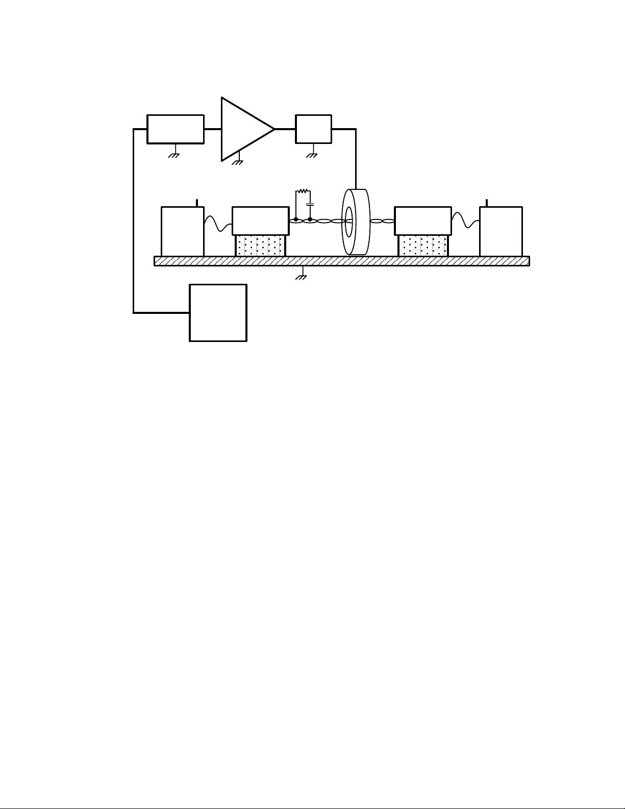
EQUIPMENT
UNDER
TEST (EUT)
HP8656B
SIGNAL
GENERATOR
75W
POWER
AMP
GROUND PLANE
TEST
CONTROL
COMPUTER
FCC
CDN - M3
50Ω
AUXILIARY
EQUIPMENT
(AE)
Dressler
Alpha 250 / 75W
-6dB
75W
PAD
EMCO
ATT 6 / 75
FCC
CDN - M3
EUT
POWER
AE
POWER
GPIB
50Ω
FCC BCI - Fischer Custom Communications
Bulk Current Injection Probe P/N F-120-9A
FCC CDN M3 - Fischer Custom Communications
Coupling De-Coupling Network P/N FCC-801-M3-16A
UTP
FCC
BCI
Termination
For the EN 61000-4-6 tests, the EUT is placed on a 10 cm high, non-conducting support on
top of a metal ground plane. If the chassis of the EUT is connected to Earth ground in
typical installations, for the test it should be connected directly to the metal ground plane
with a short wire. If the EUT is left floating in normal use, there should be no connection
between the EUT and Earth ground for the EN 61000-4-6 tests.
Power connections for the auxiliary equipment and EUT should be routed through suitable
decoupling devices, such as non-driven M3 “coupling-decoupling” network (CDN) devices.
During the network immunity tests, any I/O lines that come out of the auxiliary equipment
or the EUT should also pass through a decoupling network. The objective of the BCI current
clamp is to drive the large common- mode noise signal into the network cable of the EUT.
The M3 CDNs ensure that the power supply inputs to the auxiliary equipment and EUT are
not an RF return path.
For shielded twisted-pair (STP) networks, the BCI current clamp injects common-mode noise
into the STP cable. The cable shield should be connected to Earth ground with a parallel
resistor and capacitor as shown in Figure 34. The resistor is generally 470 kΩ, 0.25 W, 5%.
The capacitor is generally 0.1 μF, 10%, metal polyester, with a voltage rating of 100 VDC or
higher.
Figure 33. Typical EN 61000-4-6 Test Setup for Unshielded Twisted-Pair (UTP) Wires
84 Design and Test for Electromagnetic Compatibility
Page 97
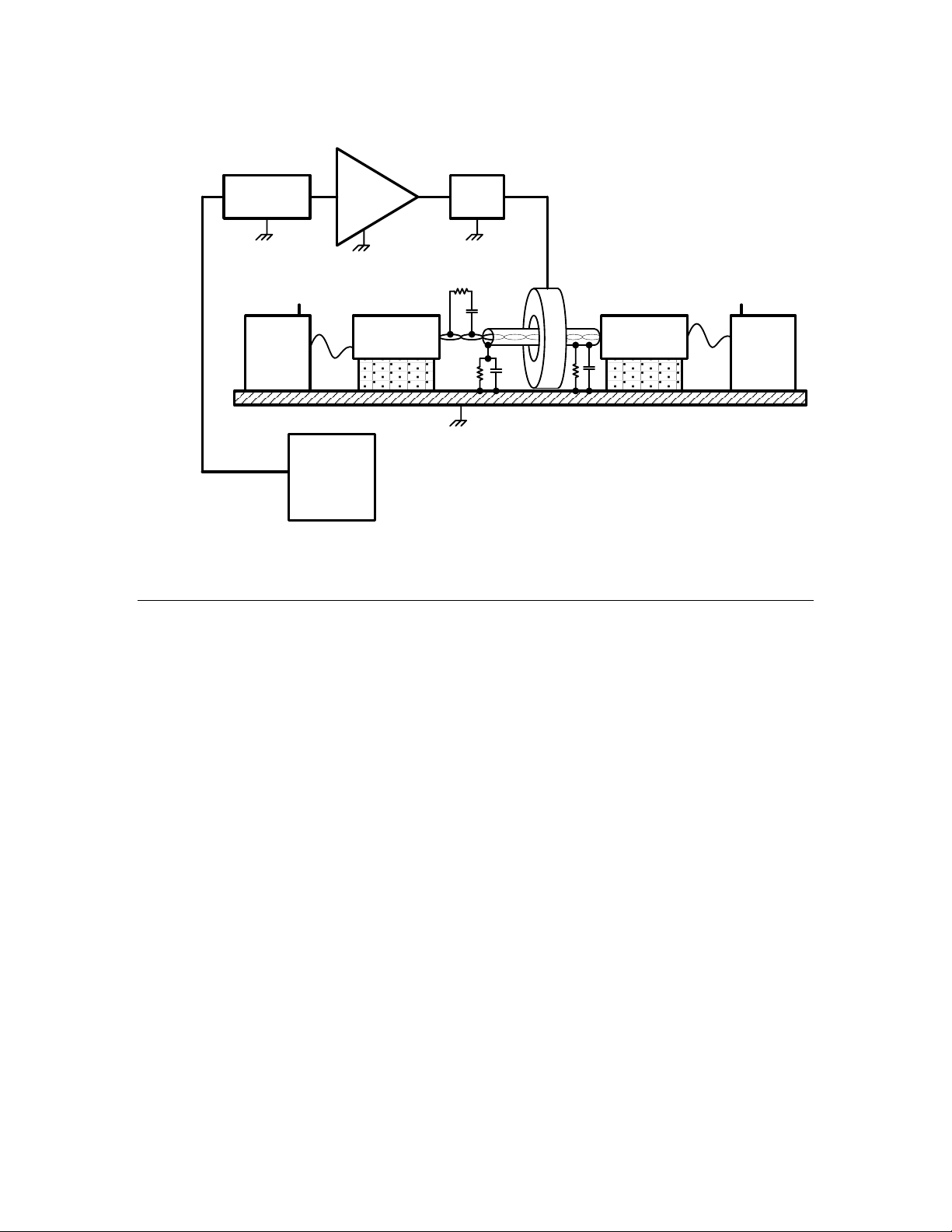
EQUIPMENT
UNDER
TEST (EUT)
HP8656B
SIGNAL
GENERATOR
75W
POWER
AMP
GROUND PLANE
TEST
CONTROL
COMPUTER
FCC
CDN - M3
50Ω
AUXILIARY
EQUIPMENT
(AE)
Dressler
Alpha 250 / 75W
-6dB
75W
PAD
EMCO
ATT 6 / 75
FCC
CDN - M3
EUT
POWER
AE
POWER
GPIB
50Ω
FCC BCI - Fischer Custom Communications
Bulk Current Injection Probe P/N F-120-9A
FCC CDN M3 - Fischer Custom Communications
Coupling De-Coupling Network P/N FCC-801-M3-16A
STP
FCC
BCI
Termination
Surge and Burst
For the purposes of EMC testing, a surge is a transient overvoltage of several kV with a rise
time that is measured in microseconds or nanoseconds, and with a duration that is measured
in microseconds. Compared with fast transient bursts and ESD, surges are relatively slow,
but also long lived.
A surge is created by a switching event or insulation fault in the AC power distribution
network, or by the switching of a reactive load (such as an electric motor). A surge can also
be caused by lightning, but EN 61000-4-5 only indirectly addresses the effects of lightning.
EN 61000-4-5 Surge testing is performed on a non-conducting table using specialized surge
generation equipment. The surges are injected directly into the network wiring (in a
common-mode fashion) or into the power supply cable through a coupling circuit. During the
test, the device should continue to operate normally, with occasional packet loss due to the
surges.
There are three levels of network testing that are relevant to Series 6000 devices:
EN 61000-4-4 Burst testing of the network cable is performed on a non-conducting table,
with 1 meter of the network cable clamped in a high-voltage burst generation apparatus.
The test capacitively injects high voltage bursts of noise into the network cable. The test
injects three bursts onto the network cable each second. During the test, the device should
continue to operate normally, with occasional packet loss due to the bursts.
Figure 34. Typical EN 61000-4-6 Test Setup for Shielded Twisted-Pair (STP) Wires
• Level 2 conductively couples a ±1 kV surge into the network
• Level 3 conductively couples a ±2 kV surge into the network
• Level “X” conductively couples a user-defined surge voltage into the network
Series 6000 Chip Data Book 85
Page 98

There are two levels of network testing that are relevant to Series 6000 devices:
• Level 3, which represents a typical industrial environment, injects ±1 kV bursts
continuously for 60 seconds
• Level 4 which represents a severe industrial environment, injects ±2 kV bursts
continuously for 60 seconds
In addition, burst testing is performed on the power supply input cable. For Series 6000
devices, the following levels of power supply input testing are relevant:
• Level 3, which represents a typical industrial environment, injects ±2 kV bursts
continuously for 60 seconds
• Level 4 which represents a severe industrial environment, injects ±4 kV bursts
continuously for 60 seconds
Lightning Protection
Protection against lightning is required when designing control networks that run outside of
buildings.
Building Entran c e Protection
Echelon recommends using shielded twisted-pair wire for all networks, or portions of
networks, that are run outside of buildings or grounded structures. The shield, as well as
the two network lines, should be connected to Earth ground through Data Line
Lightning/Surge arresters at each building entry point. This connection conducts excessive
energy surges or lightning strike energy directly to Earth and prevents their entry inside the
building through the network shield or data line conductors. Therefore, three arresters
should be used at each building entrance for shielded twisted-pair wiring.
Network Line Prot ection
The arresters used on the network data lines must be of the Gas Discharge type. The
intrinsically low capacitance to ground of these devices, typically less than 5 pF, minimizes
the corruption of any data signals. Due to their low capacitance construction, the use of Gas
Discharge devices does not alter the maximum number of devices allowed per network
segment.
Important: MOV and TVS protection devices must not be used on the network data lines
because of their much higher capacitance (>200 pF) and potentially poor differential
capacitance matching. These devices can corrupt, and possibly prevent, network
communication between devices.
Shield Protecti on
Gas Discharge, MOV, or TVS devices can be used for the shield-to-ground protection.
MOV and TVS devices should not be used to protect the network data lines.
Suggested Gas Dis c harge Arresters
Three-electrode device configurations are suggested for the data network lines, because they
require the use of only one physical device to protect both lines. The network lines should be
connected to the two outside ends of the arrester, while the middle terminal must be
86 Design and Test for Electromagnetic Compatibility
Page 99
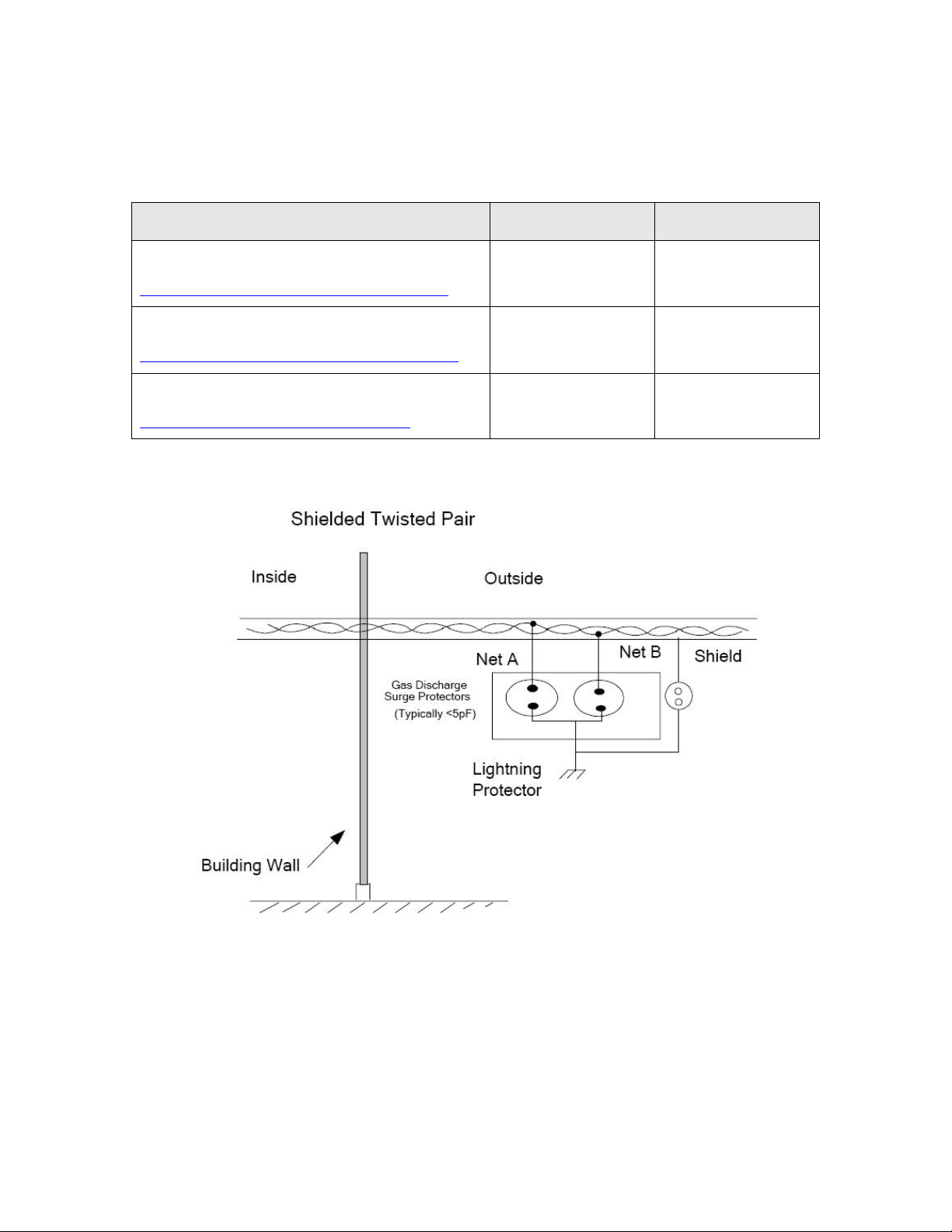
connected to a stable Earth ground. Alternatively, two each of two-electrode configurations
can be used (contact manufacturer for details). Table 25 provides a list of three-electrode
Gas Discharge device manufacturers.
Table 25. Manufactures of Suggested Gas Discharge Arresters
Vendor and Configuration Series Voltage
Sankosha, 3 Electrode
www.sankosha-usa.com/arresters.asp?id=2
Citel, 3 Electrode
www.citelprotection.com/citel/gas_cover.htm
Littelfuse, 3 Electrode
www.littelfuse.com/series/PMT8.html
Figure 35 shows a typical outdoor twisted pair network in which Gas Discharge arresters
have been incorporated.
3H or 3P 90 VDC
BT, BTR, or BTS 90 VDC
PMT8 90 VDC
Figure 35. Network and Shield Lightning Protection
When the network data line extends outside of a building or grounded structure, every FT
6000 Smart Transceiver or Neuron 6000 Processor device on the network segment, whether
located indoors or outdoors, must be equipped with surge protection circuitry. Additionally,
protection devices must be added to the network at every point where the network cable exits
the building or structure.
Series 6000 Chip Data Book 87
Page 100

Avoiding Magnetic Field Interference
All transformer-based transceivers are vulnerable to stray magnetic fields that can interfere
with the transformer coupling. In most environments, stray magnetic field noise is not a
concern for FT 6000 Smart Transceivers or Neuron 6000 Processors with external
transceivers. However, high frequency external magnetic fields can couple sufficient energy
into the transceiver to cause erratic network performance or, in some cases, cause data
traffic to cease.
One possible source of stray magnetic fields is a DC-DC switching power supply, or regulator,
using unshielded switching inductors located in close proximity to the transceiver. To
minimize magnetic coupling into the transceiver, the switching magnetics of power supplies
should be kept at least 7.5 cm (3 inches) from the FT 6000 Smart Transceiver or Neuron
6000 Processor with external transceiver. Otherwise, noise induced into the receiver could
affect communications.
If you suspect magnetic field interference, you should measure the level of noise at the FT
6000 Smart Transceiver or Neuron 6000 Processor with external transceiver. You can
measure the noise induced by a switching power supply by using an oscilloscope with
differential probes having at least 5 V common-mode range with 50 dB of common-mode
rejection to measure the voltage between the Series 6000 chip’s NETP and NETN pins
during an interval when there is no packet activity. You can also identify the source of the
magnetic noise by moving the suspected source away from the FT 6000 Smart Transceiver or
Neuron 6000 Processor with external transceiver by connecting it to at least 15 cm twistedpair wires and monitoring the noise at the NETP and NETN pins.
The noise between the NETP and NETN pins should be less than 15 mV peak-to-peak
differential. For noise that is magnetically coupled from a switching power supply, the noise
will be synchronous with the power supply switching frequency. The worst case occurs when
the coupled noise is between 10 kHz and 300 kHz, the center of the network data
communication band. If the noise is greater than 15 mV peak-to-peak, you should take steps
to reduce the coupling effect. The easiest solution is to provide more distance between the
power supply and the FT 6000 Smart Transceiver or Neuron 6000 Processor with external
transceiver.
For noisy power converters, shielded inductors can provide a solution to magnetic field
interference. In the commonly used buck DC-DC converter, a shielded inductor can be used
instead of an open-slug inductor to significantly lower the amount of stray magnetic field
generated by the DC-DC converter. For example, Taiyo Yuden’s LHFP-series inductor can
be used instead of their LHL-series, and TDK’s FS-series inductor can be used instead of
their EL or ELF-series. In transformer-based DC-DC converters, the power supply designer
should take care to choose a transformer style that generates minimum external stray
magnetic fields. For example, a pot-core DC-DC transformer will generally produce less
stray magnetic field than will an E-E core transformer, and the stray fields that it does
generate are vertical when they go through the plane of the PCB. A common way to
minimize magnetic fields emitted from power supply transformers is to wrap a “shortedturn” of copper tape around the transformer in the same direction as the transformer
winding.
In addition to power supplies, other noise sources can include DC motor controllers and
industrial ovens or heaters. For these noise sources, shielding the emitting device is often
the most effective approach to solving magnetic field interference problems.
88 Design and Test for Electromagnetic Compatibility
 Loading...