

Page 1

EV8AQ160-EB Evaluation Board
..............................................................................................
User Guide
Page 2

Page 3

Table of Contents
Section 1
1.1 Scope........................................................................................................1-3
1.2 Description ................................................................................................1-3
Section 2
2.1 Board Structure .........................................................................................2-5
2.2 Analog Inputs/Clock Input .........................................................................2-6
2.3 Digital Output ............................................................................................2-6
2.4 Reset Inputs ..............................................................................................2-7
2.5 Power Supplies .........................................................................................2-9
Section 3
3.1 Introduction .............................................................................................3-11
3.2 Operating Procedure...............................................................................3-11
3.3 Electrical Characteristics.........................................................................3-12
Section 4
4.1 Overview .................................................................................................4-15
4.2 Configuration...........................................................................................4-15
4.3 Getting Started ........................................................................................4-15
4.4 Troubleshooting ......................................................................................4-22
4.5 Installation Software................................................................................4-23
4.6 Operating Modes ....................................................................................4-24
4.6.1 Settings.............................................................................................4-25
4.6.2 Test...................................................................................................4-29
4.6.3 Gain/Offset/Phase ............................................................................4-30
4.7 INL ..........................................................................................................4-33
4.7.1 INL Calibration Procedure ................................................................4-34
4.8 Input Impedance .....................................................................................4-39
Section 5
5.1 Analog Input............................................................................................5-43
5.2 ..............................................................................................Clock Input5-44
5.3 RESET input ...........................................................................................5-44
5.4 Output Data.............................................................................................5-45
5.5 CMIRefAB and CMIRefCD Output Signals .............................................5-45
5.6 Diode for Junction Temperature Monitoring............................................5-45
5.7 Test Bench Description ...........................................................................5-46
Section 6
EV8AQ160-EB - User Guide i
0834E–BDC–07/09
e2v semiconductors SAS 2009
Page 4

6.1 Ordering Information ...............................................................................6-47
Section 7
7.1 EV8AQ160-EB Electrical Schematics .....................................................7-49
7.2 EV8AQ160-EB Board Layers..................................................................7-53
ii EV8AQ160-EB - User Guide
0834E–BDC–07/09
e2v semiconductors SAS 2008
Page 5

Section 1
Introduction
1.1 Scope The EV8AQ160-EB Evaluation Kit is designed to facilitate the evaluation and character-
ization of the EV8AQ160 Quad 8-bit 1.25 Gsps ADC in AC coupled mode.
The EV8AQ160-EB Evaluation Kit includes:
The Quad 8-bit 1.25 Gsps ADC Evaluation Board including EV8AQ160 ADC and
Atmel ATMEGA128 AVR soldered
A cable for connection to the RS-232 port
Software Tools necessary to use the SPI
The user guide uses the EV8AQ160-EB Evaluation Kit as an evaluation and demonstration platform and provides guidelines for its proper use.
1.2 Description The EV8AQ160-EB Evaluation Board is very straightforward as it implements e2v
EV8AQ160 Quad 8-bit 1.25 Gsps ADC device, Atmel ATMEGA128 AVR, SMA connec
tors for the sampling clock, analog inputs and reset inputs accesses and 2.54 mm pitch
connectors compatible with high-speed acquisition system probes.
-
Thanks to its user-friendly interface, the EV8AQ160-EB Kit enables to test all the functions of the EV8AQ160 Quad 8-bit 1.25 Gsps ADC using the SPI connected to a PC.
To achieve optimal performance, the EV8AQ160-EB Evaluation Board was designed in
a 6-metal-layer board using FR4 HTG epoxy dielectric material (200 µm, ISOLA IS410
featuring a resin content of 45%). The board implements the following devices:
The Quad 8-bit 1.25 Gsps ADC Evaluation Board with the EV8AQ160 ADC soldered
SMA connectors for CLK, CLKN, AAI, AAIN, BAI, BAIN, CAI, CAIN, DAI, DAIN,
SYNCP, SYNCN, CAL, CALN signals
2.54 mm pitch connectors for the digital outputs, compatible with high speed
acquisition system probes
Banana jacks for the power supply accesses, the die junction temperature monitoring
functions, reference resistor, analog input common mode voltage (2 mm)
An RS-232 connector for PC interface
EV8AQ160-EB - User Guide 1-3
0834E–BDC–07/09
e2v semiconductors SAS 2009
Page 6
Introduction
C
O
R
D
O
R
D
L
P
O
R
T
C
O
R
O
R
B
H
P
O
R
T
O
R
O
R
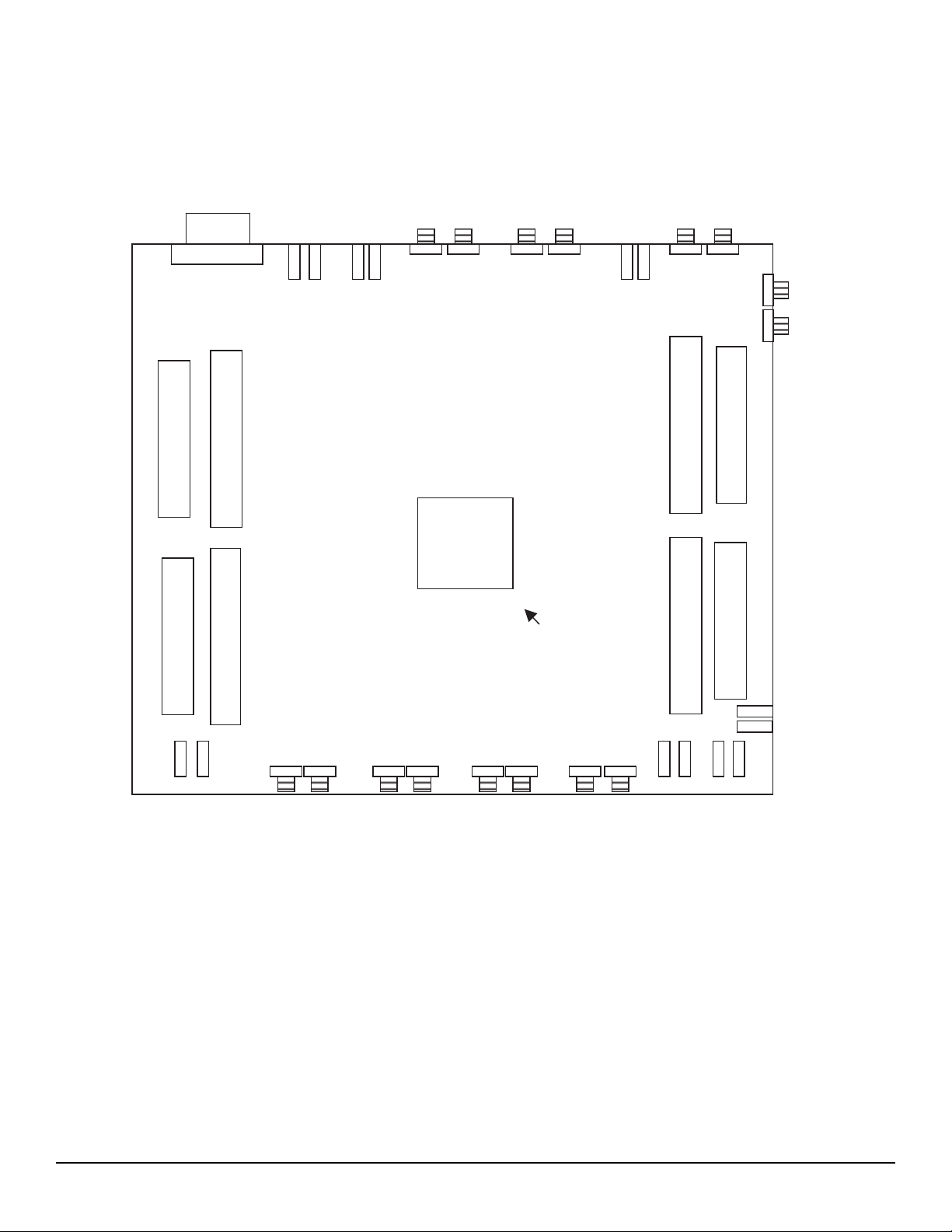
The board dimensions are 170 mm x 185 mm.
The board comes fully assembled and tested, with the EV8AQ160 installed.
Figure 1-1. EV8AQ160-EB Evaluation Board Simplified Schematic
RS232
H
P
T
H
P
T
L
P
T
3.3V GND
Res62
Res50
CLKN CLK
EV8AQ160
SYNCP SYNCN
DiodC
DiodA
CALN CAL
B
L
P
T
A
L
P
T
CAL
CALN
A
H
P
T
VCCD
GND
AAI AAIN BAI
GND
VCCO
GND
VCC
CMIREFCD
CMIREFAB
CAI CAIN DAI DAIN
BAIN
As shown in Figure 1-1, different power supplies are required:
VCC = 3.3V analog positive power supply (includes the SPI pads)
V
V
= 1.8V digital positive power supply
CCD
= 1.8V output power supply
CCO
3.3V digital interface primary power supply for the microcontroller
1-4 EV8AQ160-EB - User Guide
0834E–BDC–07/09
e2v semiconductors SAS 2009
Page 7

Section 2
Hardware Description
2.1 Board Structure In order to achieve optimum full-speed operation of the EV8AQ160 Quad 8-bit 1.25
Gsps ADC, a multilayer board structure was retained for the evaluation board. Six cop
per layers are used, dedicated to the signal traces, ground planes and power supply
planes.
The board is made in FR4 HTG epoxy dielectric material (ISOLA IS410).
The following table gives a detailed description of the board's structure.
Table 2-1. Board Layer Thickness Profile
Layer Characteristics
Copper thickness = 40 µm (with NiAu finish)
Layer 1
Copper layer
FR4 HTG/dielectric layer Layer thickness = 200 µm
Layer 2
Copper layer
FR4 HTG/dielectric layer Layer thickness = 349 µm
Layer 3
Copper layer
FR4 HTG/dielectric layer Layer thickness = 350 µm
AC signals traces = 50Ω microstrip lines
DC signals traces
Copper thickness = 18 µm
Upper ground plane = reference plane
Copper thickness = 18 µm
Power plane = V
CC
-
Layer 4
Copper layer
FR4 HTG/dielectric layer Layer thickness = 350 µm
Layer 5
Copper layer
FR4 HTG/dielectric layer Layer thickness = 200 µm
Layer 6
Copper layer
EV8AQ160-EB - User Guide 2-5
Copper thickness = 18 µm
Power planes = V
Copper thickness = 18 µm
Power planes = reference plane (identical to layer 3)
Copper thickness = 40 µm (with NiAu finish)
AC signals traces = 50Ω microstrip lines
DC signals traces
CCD’ VCCO
and 3V3
0834E–BDC–07/09
e2v semiconductors SAS 2008
Page 8
Hardware Description
The board is 1.6 mm thick.
The Clock, analog inputs, resets, digital data output signals (port H) and ADC functions
occupy the top metal layer, while the output data of the L ports and the SPI signals and
circuitry occupy the bottom layer.
The ground planes occupy layer 2 and 5.
Layer 3 and 4 are dedicated to the power supplies.
2.2 Analog Inputs/Clock Input
The differential clock and analog inputs are provided by SMA connectors (Reference:
VITELEC 142-0701-8511).
Both pairs are AC coupled using 10 nF capacitors.
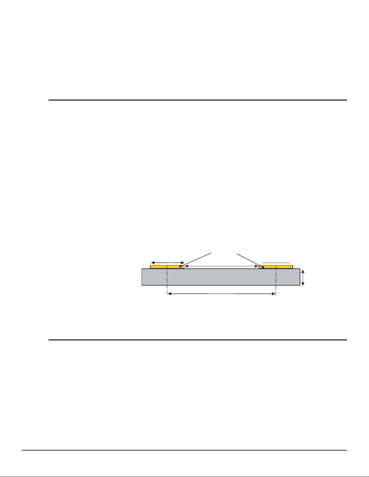
Special care was taken for the routing of the analog and clock input signals for optimum
performance in the high frequency domain:
50Ω lines matched to ±0.1 mm (in length) between XAI and XAIN (X = A, B, C or D) or
CLK and CLKN
909 µm pitch between the differential traces
1270 µm between two differential pairs
361 µm line width
40 µm thickness
850 µm diameter hole in the ground layer below the XAI and XAIN or CLK and CLKN
ball footprints
Figure 2-1. Board Layout for the Differential Analog and Clock Inputs
e = 40 µm
361 µm 361 µm
909 µm
FR4 HTG
200µm
1270 µm
Note: The analog inputs and clock inputs are AC coupled with 10 nF very close to the SMA
connectors.
2.3 Digital Output The digital output lines were designed with the following recommendations:
50Ω lines matched to ±2.5 mm (in length) between signal of the same differential pair
±1mm line length difference between signals of two differential pairs
635 µm pitch between the differential traces
650 µm between two differential pairs
310 µm line width
40 µm thickness
2-6 EV8AQ160-EB - User Guide
0834E–BDC–07/09
e2v semiconductors SAS 2009
Page 9
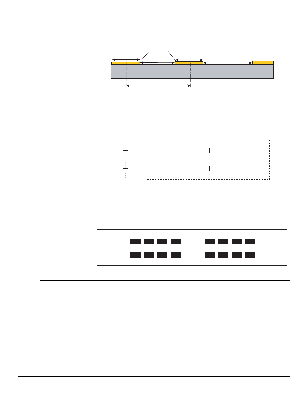
Figure 2-2. Board Layout for the Differential Digital Outputs
e = 40 µm
310 µm 310 µm
325 µm
650 µm
Hardware Description
FR4 HTG
635 µm
200 µm
The digital outputs are compatible with LVDS standard. They are on-board 100Ω differentially terminated as described in Figure 2-3.
Figure 2-3. Differential Digital Outputs Implementation
Connector
100Ω
ADC
Double row 2.54 mm pitch connectors are used for the digital output data. The upper
row is connected to the signal while the lower row is connected to Ground, as illustrated
in
Figure 2-4.
Figure 2-4. Differential Digital Outputs 2.54 mm Pitch Connector (X = AL, AH, BL, BH,
CL, CH, DL, DH)
XDR XDRN XD0
GND GND GND GND GND GND GND GND
XD0N XD7 XD7N XORNNXOR
2.4 Reset Inputs Two hardware reset signals are provided:
– SYNCP, SYNCN corresponds to the reset of the output clock of the ADC
(analog reset).
– RSTN corresponds to the reset of the SPI (makes the SPI registers go to their
default value).
The differential reset inputs SYNC, SYNCN are provided by SMA connectors (reference: VITELEC 142-0701-8511).The signals are AC coupled using 10 nF capacitors
and pulled up and down via 200Ω resistors. A variable resistor of 500Ω is implemented
on SYNC: by adjusting this resistor value one can activate and deactivate easily the
reset signal.
EV8AQ160-EB - User Guide 2-7
0834E–BDC–07/09
e2v semiconductors SAS 2009
Page 10
Hardware Description
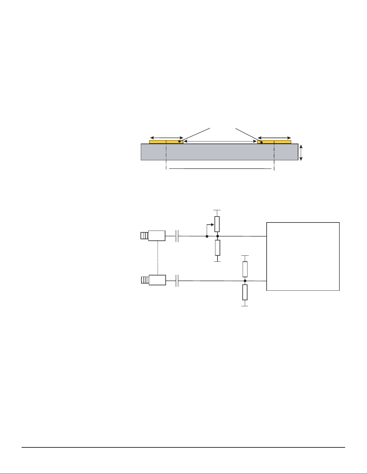
50Ω lines matched to ±0.1 mm (in length) between SYNCP and SYNCN
909 µm pitch between the differential traces
1270 µm between two differential pairs
361 µm line width
40 µm thickness
Figure 2-5. Board Layout for the SYNC Signal
e = 40 µm
361µm
909 µm
361µm
FR4 HTG
1270 µm
200 µm
Figure 2-6. SYNC, SYNCN Inputs Implementation
3.3V
Ω
GND
500
200
Ω
SYNC (AC11)
3.3V
GND
200
200
Ω
SYNCN (AD11)
Ω
EV8AQ160
10 nF
SYNC
SYNCN
10 nF
The resistors are used only for pull-up and pull-down of the SYNC signals. A push button is provided for the RSTN reset, as described in Figure 2-7 on page 2-9. This reset
can also be generated through the AVR (via the User Interface).
2-8 EV8AQ160-EB - User Guide
0834E–BDC–07/09
e2v semiconductors SAS 2009
Page 11
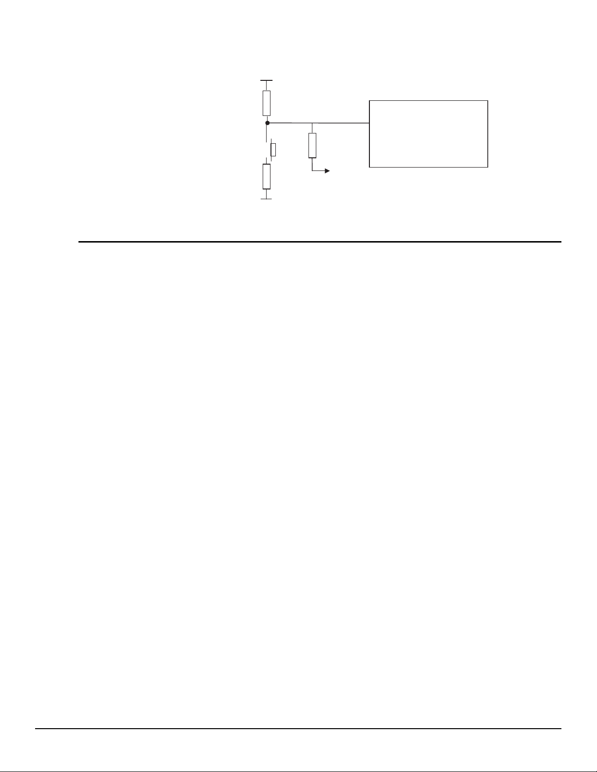
Figure 2-7. RSTN Input Implementation
3.3V
10K
Ω
Hardware Description
RSTN (AC15)
0
Ω
To AVR
GND
0
Ω
2.5 Power Supplies Layers 3 and 4 are dedicated to power supply planes (V
The supply traces are low impedance and are surrounded by two ground planes (layer 2
and 5).
Each incoming power supply is bypassed at the banana jack by a 1 µF Tantalum capacitor in parallel with a 100 nF chip capacitor.
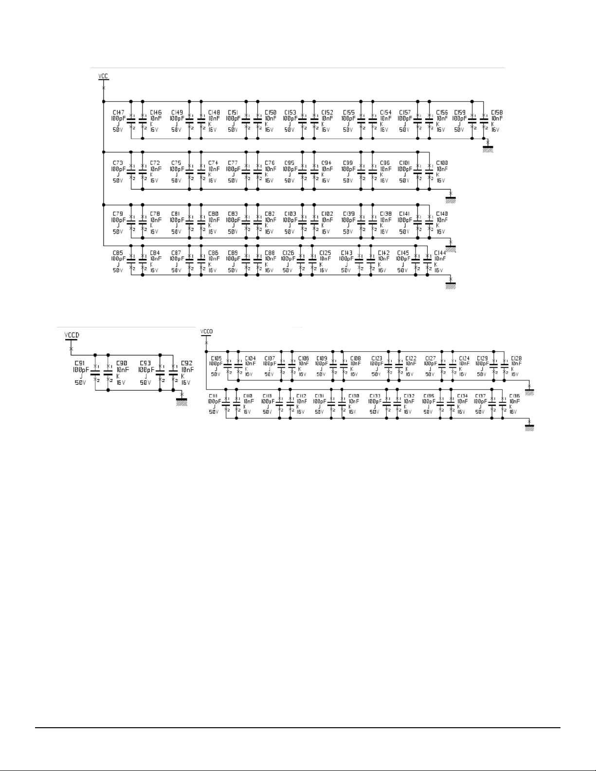
Each power supply is decoupled as close as possible to the EV8AQ160 device by 10 nF
in parallel with 100 pF surface mount chip capacitors.
Note: The decoupling capacitors are superimposed with the 100 pF capacitor mounted first.
EV8AQ160
, V
CC
CCD
, V
CCO
and 3.3V).
EV8AQ160-EB - User Guide 2-9
0834E–BDC–07/09
e2v semiconductors SAS 2009
Page 12

Hardware Description
2-10 EV8AQ160-EB - User Guide
0834E–BDC–07/09
e2v semiconductors SAS 2009
Page 13

Section 3
Operating Characteristics
3.1 Introduction This section describes a typical configuration for operating the evaluation board of the
EV8AQ160 Quad 8-bit 1.25 Gsps ADC.
The analog input signals and the sampling clock signal should be accessed in a differential fashion. Band pass filters should also be used to optimize the performance of the
ADC both on the analog input and on the clock.
It is necessary to use a very low jitter source for the clock signal (recommended maximum jitter = 50 ps).
Note: The analog inputs and clock are AC coupled on the board.
3.2 Operating Procedure
1. Install the SPI software as described in section 4 Software Tools.
2. Connect the power supplies and ground accesses through the dedicated banana
jacks. V
3. Connect the clock input signals. Use a very low-phase noise High Frequency
generator as well as a band pass filter to optimize the clock performance. The
clock input level is typically 3 dBm and should not exceed 10 dBm (into 50
clock frequency should be set to 2.5 GHz (corresponding to 1.25 Gsps sampling
in 4-channel mode or 2.5 Gsps sampling in 2-channel mode or 5 Gsps sampling
in 1-channel mode).
4. Connect the analog input signals (the board has been designed to allow only AC
coupled analog inputs). Use a low-phase noise High Frequency generator as
well as a band pass filter to optimize the analog input performance. The analog
input Full Scale is 500mV peak-to-peak around zero (analog input providing the
Input common mode). It is recommended to use the ADC with an input signal of
-1 dBFS max (to avoid saturation of the ADC).
5. Connect the high speed acquisition system probes to the output connectors. The
digital data are differentially terminated on-board (100
probed either in differential or in single-ended mode.
6. Connect the PC's RS-232 connector to the evaluation board's serial interface.
7. Switch on the ADC power supplies (recommended power up sequence: simultaneous or in the following order: VCC = 3.3V, V
8. Turn on the RF clock generator.
9. Turn on the RF signal generator.
= 3.3V, V
CC
= 1.8V, V
CCD
= 1.8V and 3.3V.
CCO
= 1.8V, V
CCD
Ω) The
Ω) however, they can be
= 1.8V and 3.3V).
CCO
EV8AQ160-EB - User Guide 3-11
0834E–BDC–07/09
e2v semiconductors SAS 2009
Page 14
Operating Characteristics
10. Perform an analog reset (SYNC potentiometer) on the device.
11. Launch Quad-8bit.exe software.
The EV8AQ160-EB evaluation board is now ready for operation.
3.3 Electrical Characteristics
For more information, please refer to the device datasheet.
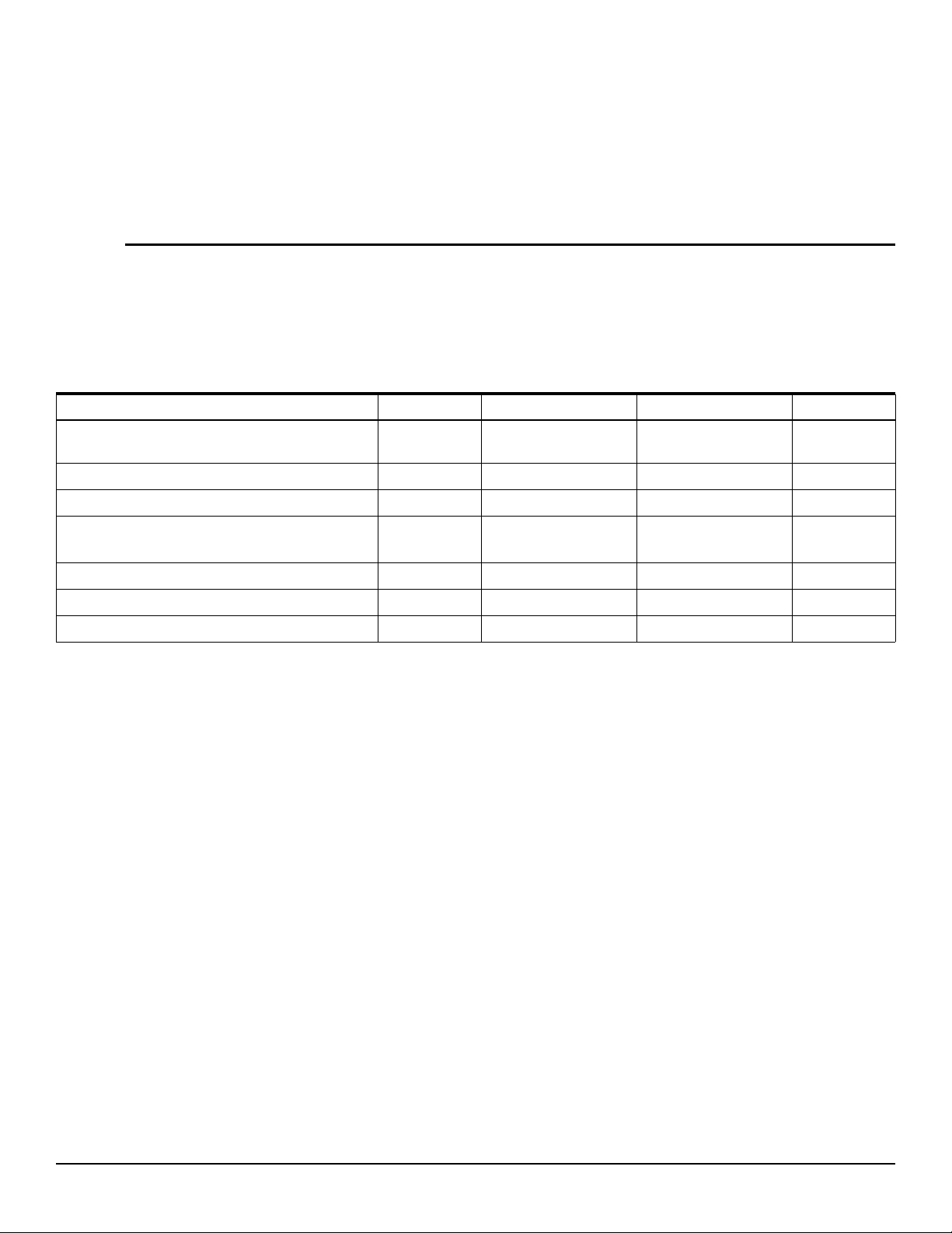
Table 3-1. Recommended Conditions of Use
Parameter Symbol Comments Recommended Unit
Analog supply voltage (includes the SPI pads
supply)
Digital supply voltage V
Output supply voltage V
Differential analog input voltage (Full Scale)
V
CC
CCD
CCO
VIN, V
VIN -V
INN
INN
Differential Clock input level with 200 fs rms jitter Vinclk 0 dBm
Analog core and SPI
pads
3.3 V
Digital parts 1.8 V
Output buffer 1.8 V
±250
500 mVpp
Operating temperature range T
Maximum Operating Junction Temperature T
Typical conditions:
VCC = 3.3V, V
V
-V
= 500 mVpp Full Scale differential input, digital outputs LVDS (100Ω)
INN
(typical) = 25°C unless otherwise specified
T
IN
amb
amb
J
CCD
= 1.8V, V
Commercial C grade 0°C < T
125 °C
= 1.8V
CCO
< 70°C °C
amb
3-12 EV8AQ160-EB - User Guide
0834E–BDC–07/09
e2v semiconductors SAS 2009
Page 15

Operating Characteristics
Table 3-2. Electrical Characteristics
Tes t
Parameter Symbol
Resolution 8Bit
Power Requirements
Power supply voltage
Analog and SPI pads
Digital
Output
V
V
V
CC
CCD
CCO
Power supply current (DMUX 1:1)
Analog and SPI pads
Digital
Output
I
CC
I
CCD
I
CCO
Power supply current (DMUX 1:2)
Analog and SPI pads
Digital
Output
I
CC
I
CCD
I
CCO
Power supply current (full standby mode,
DMUX 1:1)
Analog and SPI pads
Digital
Output and 3-Wire serial interface
I
CC
I
CCD
I
CCO
Level Min Typ Max Unit Notes
3.15
1.7
1.7
1.4 1.175
1.4
1, 4
3.3
1.8
1.8
4.9
178
1.25
4.9
300
136
4.9
29
3.45
1.9
1.9
1.3
5.5
200
1.35
5.5
350
150
5.5
45
V
V
V
A
mA
mA
A
mA
mA
mA
mA
mA
Power supply current (full standby mode,
DMUX 1:2)
Analog and SPI pads
Digital
Output and 3-Wire serial interface
Power supply current (partial standby
mode, DMUX 1:1)
Analog and SPI pads
Digital
Output and 3-Wire serial interface
Power supply current (partial standby
mode, DMUX 1:2)
Analog and SPI pads
Digital
Output and 3-Wire serial interface
Power dissipation (max. power supplies)
Full power (DMUX 1:1)
Full power (DMUX 1:2)
Partial standby (DMUX 1:1)
Partial standby (DMUX 1:2)
Full standby (DMUX 1:1)
Full standby (DMUX 1:2)
I
CC
I
CCD
I
CCO
I
CC
I
CCD
I
CCO
I
CC
I
CCD
I
CCO
P
1, 4
136
4.9
37
630
1, 4
4.9
102
1, 4 660
4.9
169
4.2
D
1, 4
4.7
2.3
2.5
0.51
0.525
150
5.5
45
700
5.5
200
750
5.5
200
4.5
4.9
2.45
2.8
0.59
0.59
mA
mA
mA
mA
mA
mA
mA
mA
mA
W
W
W
W
W
W
EV8AQ160-EB - User Guide 3-13
0834E–BDC–07/09
e2v semiconductors SAS 2008
Page 16

Operating Characteristics
3-14 EV8AQ160-EB - User Guide
0834E–BDC–07/09
e2v semiconductors SAS 2009
Page 17

Section 4
Software Tools
4.1 Overview The Quad 8-bit 1.25 Gsps ADC Evaluation user interface software is a Visual C++
compiled graphical interface that does not require a licence to run on a Windows® NT
and Windows® 2000/98/XP® PC.
The software uses intuitive push-buttons and pop-up menus to write data from the
hardware.
4.2 Configuration The advised configuration for Windows
PC with Intel® Pentium®Microprocessor of over 100 MHz
Memory of at least 24 Mo
For other versions of Windows® OS, use the recommended configuration from
Microsoft.
Note: Two COM ports are necessary to use two boards simultaneously.
®
98 is:
®
®
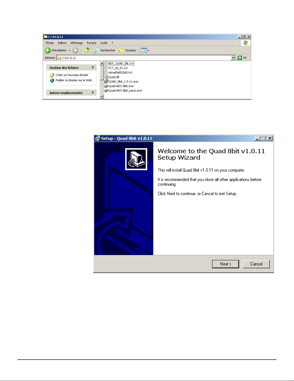
4.3 Getting Started 1. Install the ADC Quad 8-bit application on your computer by launching the
Quad_ADC_8bit_x.x.x.exe installer (please refer to the latest version available).
The screen shown in Figure 4-3 is displayed.
EV8AQ160-EB - User Guide 4-15
0834E–BDC–07/09
e2v semiconductors SAS 2009
Page 18
Software Tools
Figure 4-1. Install Window
Figure 4-2. QUAD 8-bit 1.25 Gsps Application Setup Wizard Window
4-16 EV8AQ160-EB - User Guide
0834E–BDC–07/09
e2v semiconductors SAS 2009
Page 19
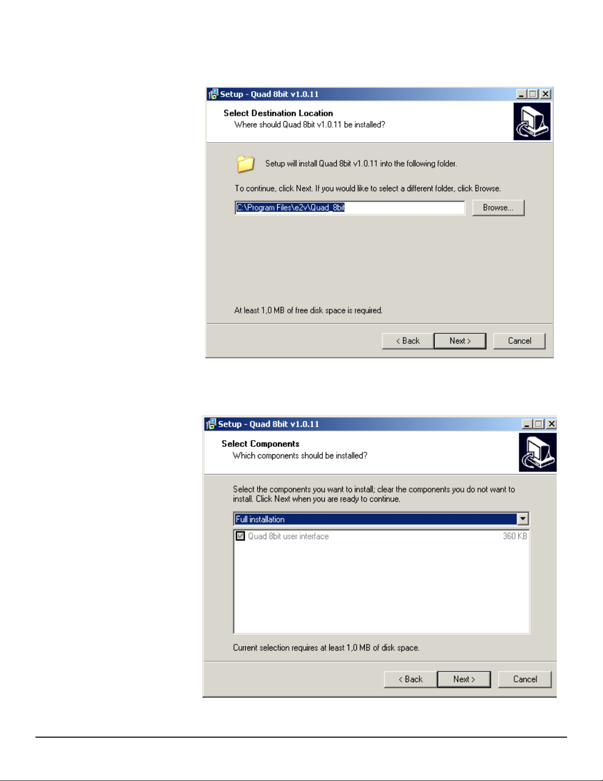
2. Select Destination Directory
Figure 4-3. QUAD 8-bit 1.25 Gsps Select Destination Directory Window
Software Tools
3. Select Components (choose Full installation)
Figure 4-4. QUAD 8-bit 1.25 Gsps Select Component Window
EV8AQ160-EB - User Guide 4-17
0834E–BDC–07/09
e2v semiconductors SAS 2009
Page 20
Software Tools
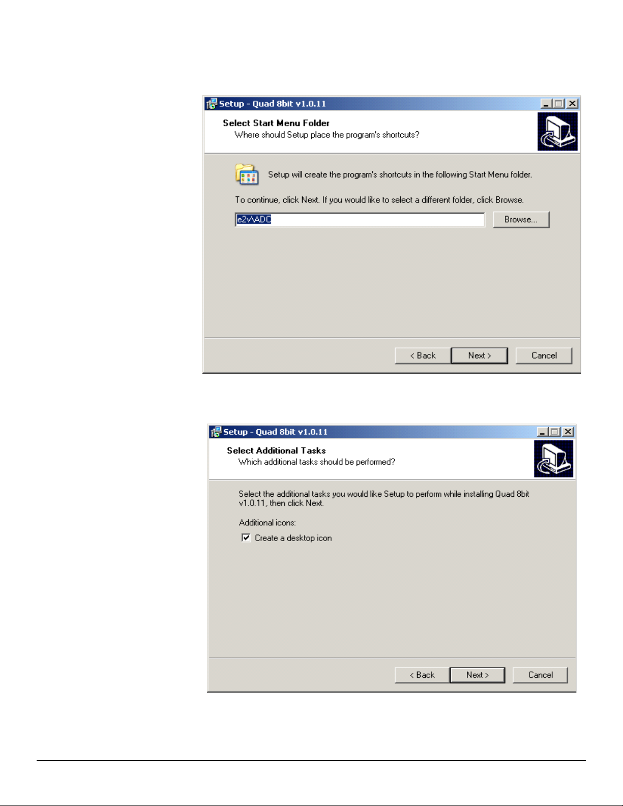
4. Select Start Menu Folder
Figure 4-5. QUAD 8-bit 1.25 Gsps Select Start Menu Window
5. Select Additional Tasks
Figure 4-6. QUAD 8-bit 1.25 Gsps Select Additional Task Window
4-18 EV8AQ160-EB - User Guide
0834E–BDC–07/09
e2v semiconductors SAS 2009
Page 21
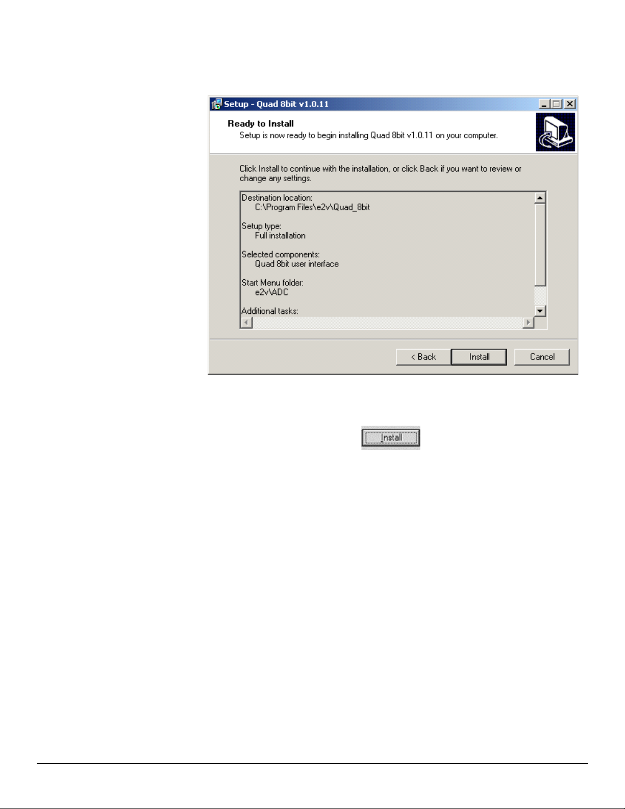
6. Ready to install
Figure 4-7. QUAD 8-bit 1.25 Gsps Ready To Install Window
Software Tools
If you agree with the install configuration, press Install button.
Figure 4-8. QUAD 8-bit 1.25 Gsps Application Setup Install Push Button
The installation of the software is now complete.
EV8AQ160-EB - User Guide 4-19
0834E–BDC–07/09
e2v semiconductors SAS 2009
Page 22
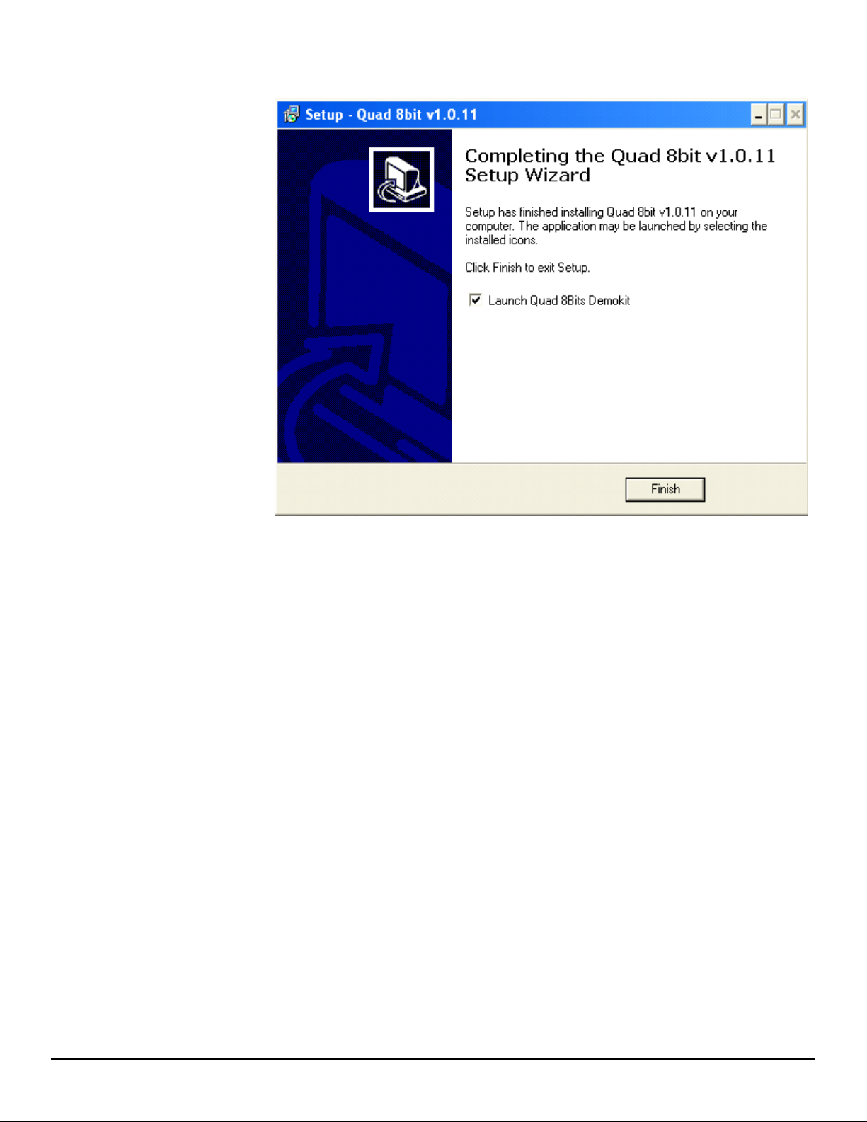
Software Tools
Figure 4-9. QUAD 8-bit 1.25 Gsps Completing Setup Wizard Window
After the installation, you can launch the interface with the following file:
C:\Program Files\e2v\QUAD_8bit\Quad ADC 8bit.exe
The window shown in Figure 4-10 will be displayed.
4-20 EV8AQ160-EB - User Guide
0834E–BDC–07/09
e2v semiconductors SAS 2009
Page 23
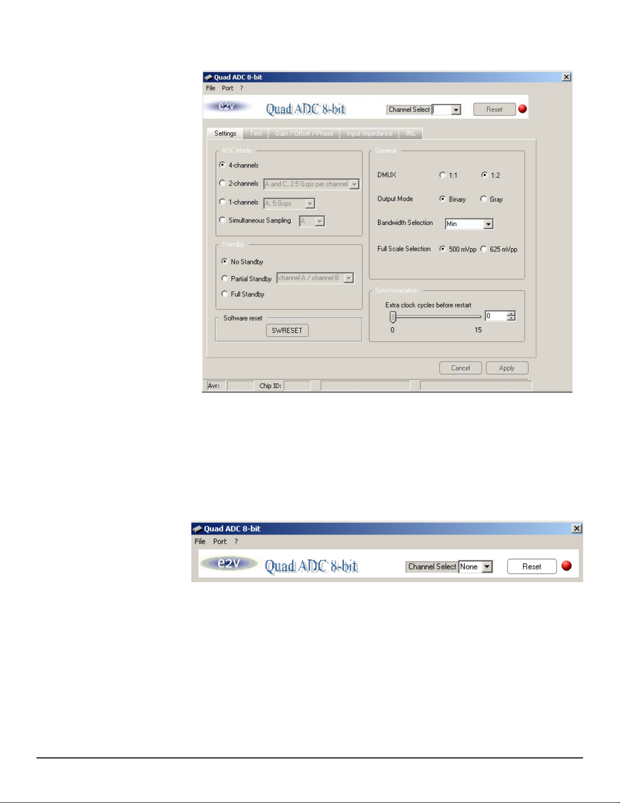
Figure 4-10. QUAD 8-bit 1.25 Gsps User Interface Window
Software Tools
Notes: 1. If the QUAD 8-bit 1.25 Gsps Application board is not connected or not powered, a red
LED appears on the right of the reset button and the application is grayed out.
2. Check your connection and restart the application.
3. If the serial interface is not active the LED appears in orange and the application is
grayed out.
Figure 4-11. QUAD 8-bit 1.25 Gsps User Interface Window
Switch ON power supplies and launch the Quad ADC 8bit.exe, the application should
become available and the LED turns to green.
EV8AQ160-EB - User Guide 4-21
0834E–BDC–07/09
e2v semiconductors SAS 2009
Page 24
Software Tools
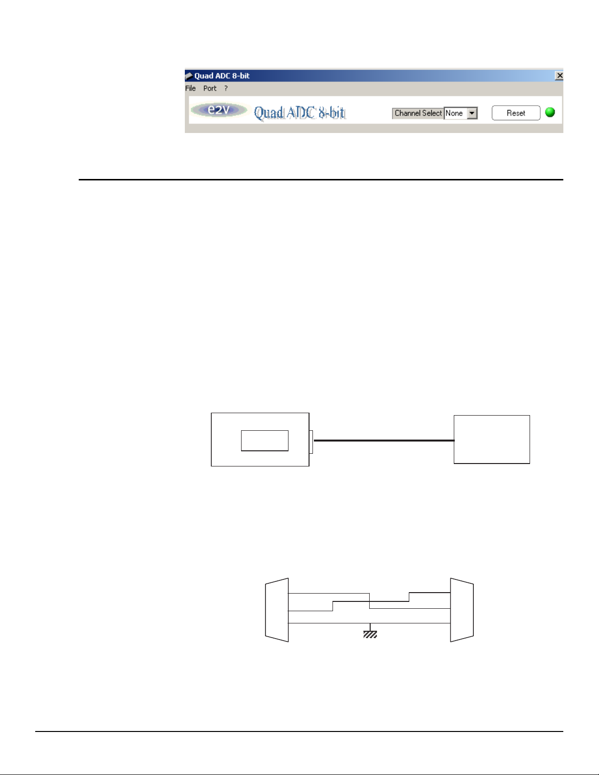
Figure 4-12. QUAD 8-bit 1.25 Gsps User Interface Window
4.4 Troubleshooting 1. check that you own rights to write in the directory.
2. check for the available disk space.
3. check that at least one RS-232 serial port is free and properly configured.
4. check that the serial port and DB9 connector are properly connected.
5. check that all supplies are properly powered on.
The serial port configuration should be as follows:
Bit rate: 19200
Data coding: 8 bits
1 start bit, 1 stop bit
No parity check
Figure 4-13. QUAD 8-bit 1.25 Gsps User Interface Hardware Implementation
PC
Software
Serial port
Evaluation Board
ADC
Quad 8-bit
1. Use an RS-232 port to send data to the ADC.
2. Connect the crossed DB9 (F/F) cable between your PC and your evaluation
board as illustrated in
Figure 4-14.
Figure 4-14. Crossed Cable
DB 9
Female
2
3
2
DB 9
Female
3
5
4-22 EV8AQ160-EB - User Guide
0834E–BDC–07/09
e2v semiconductors SAS 2009
5
Page 25
4.5 Installation Software
Software Tools
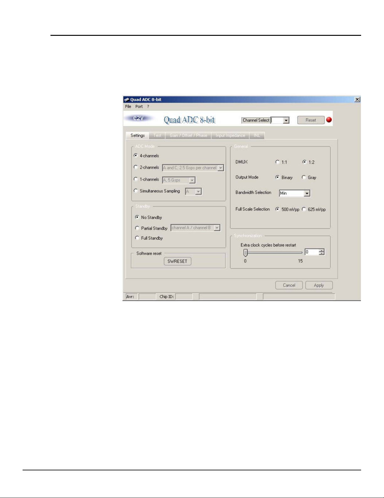
At startup, the application automatically checks all RS232 ports available on the computer and tries to find the evaluation board connected to the RS232 port.
Figure 4-15. QUAD 8-bit 1.25 Gsps User Interface Port Menu
The Port menu shows all available ports on your computer. The port currently used has
a check mark on its left. By clicking another port item the application will try to connect to
an evaluation board via the selected port. If a board is successfully detected on the new
port, the LED is green and the new port gets the check mark. If the application is not
able to find a board on this port, an error message is displayed.
EV8AQ160-EB - User Guide 4-23
0834E–BDC–07/09
e2v semiconductors SAS 2009
Page 26
Software Tools
4.6 Operating Modes
The Quad ADC software included with the evaluation board provides a graphical user
interface to configure the ADC.
Push buttons, popup menus and capture windows allows easy:
1. Settings.
2. Test mode.
3. Gain/Offset/Phase adjustments.
4. INL adjustments.
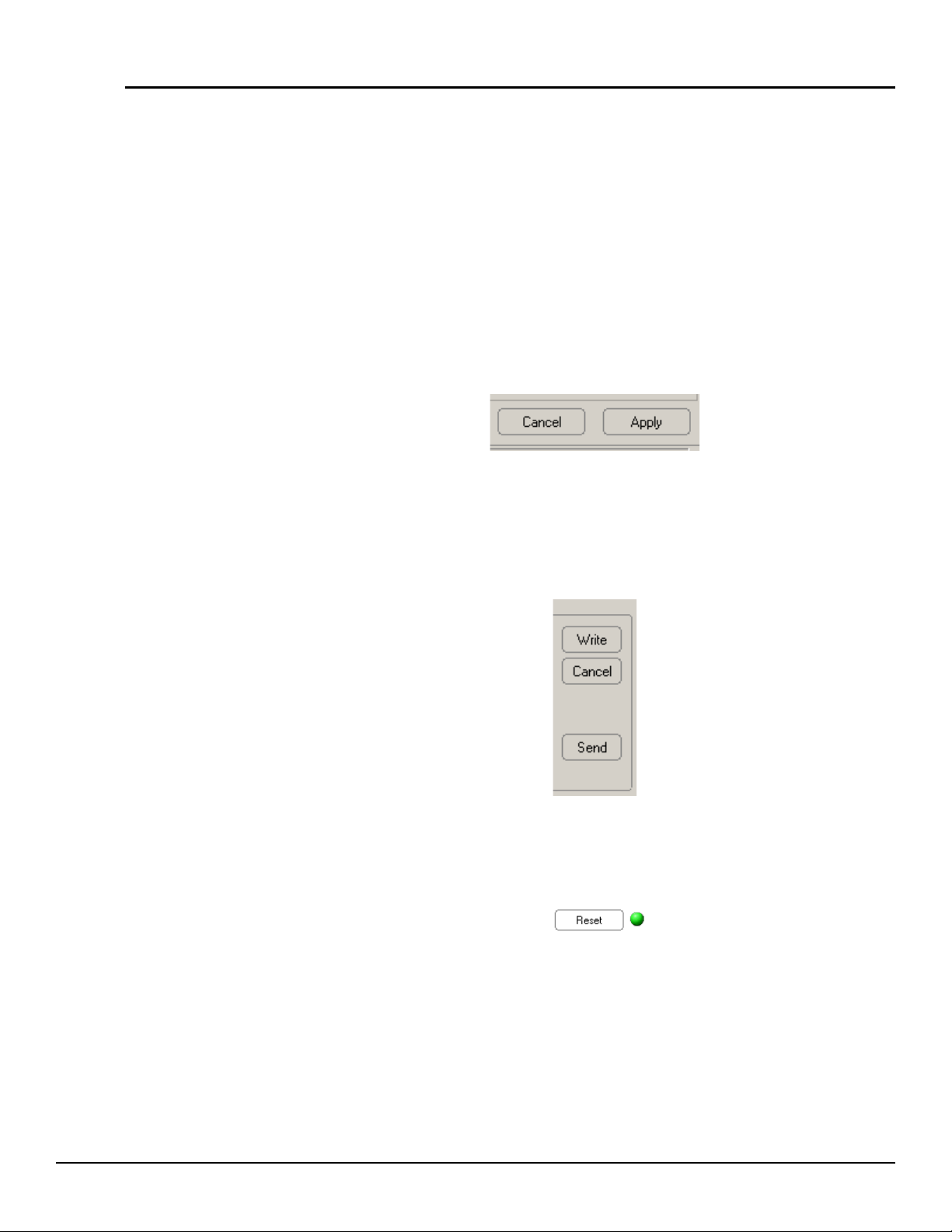
With Setting and Test mode windows always click on Apply button to validate any
command.
Clicking the Cancel button will restore last settings sent with Apply button.
With Gain/Offset/Phase and INL windows always click on Write then Send buttons to
validate any command.
Reset button allows reconfiguring ADC to Default Mode.
4-24 EV8AQ160-EB - User Guide
0834E–BDC–07/09
e2v semiconductors SAS 2009
Page 27
4.6.1 Settings
Software Tools
or
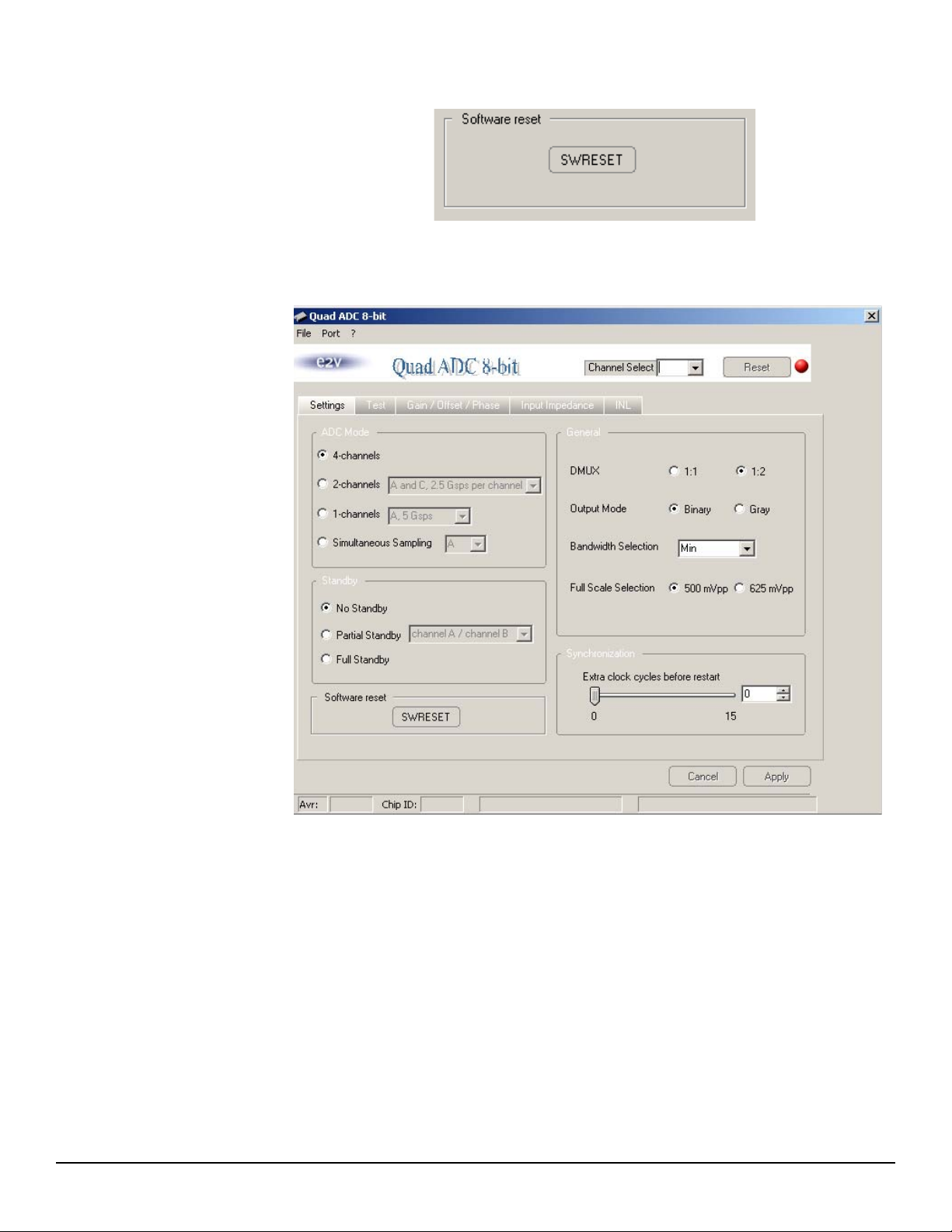
Figure 4-16. Settings
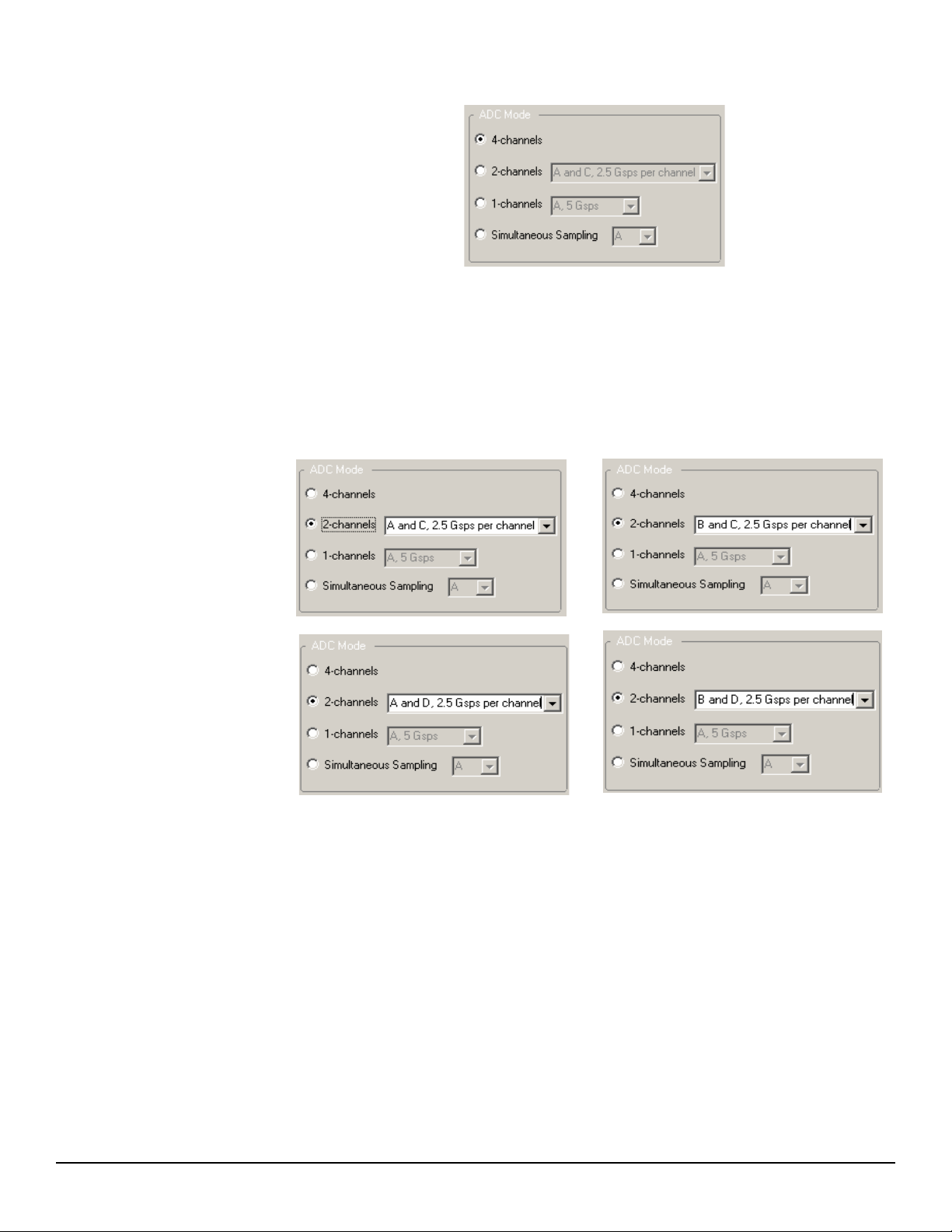
In this window, five functions are available:
ADC mode:
– 4-channel mode = the four ADCs work independently at Fclock/2 sampling
rate (where Fclock is the external clock signal frequency).
EV8AQ160-EB - User Guide 4-25
0834E–BDC–07/09
e2v semiconductors SAS 2009
Page 28
Software Tools
– Two-channel mode = the four ADCs are interleaved two by two (A and B, C
and D), the sampling rate is equal to Fclock (where Fclock is the external clock
signal frequency), the analog inputs can be applied to A or B and respectively
C or D.
Figure 4-17. Two Channel Mode
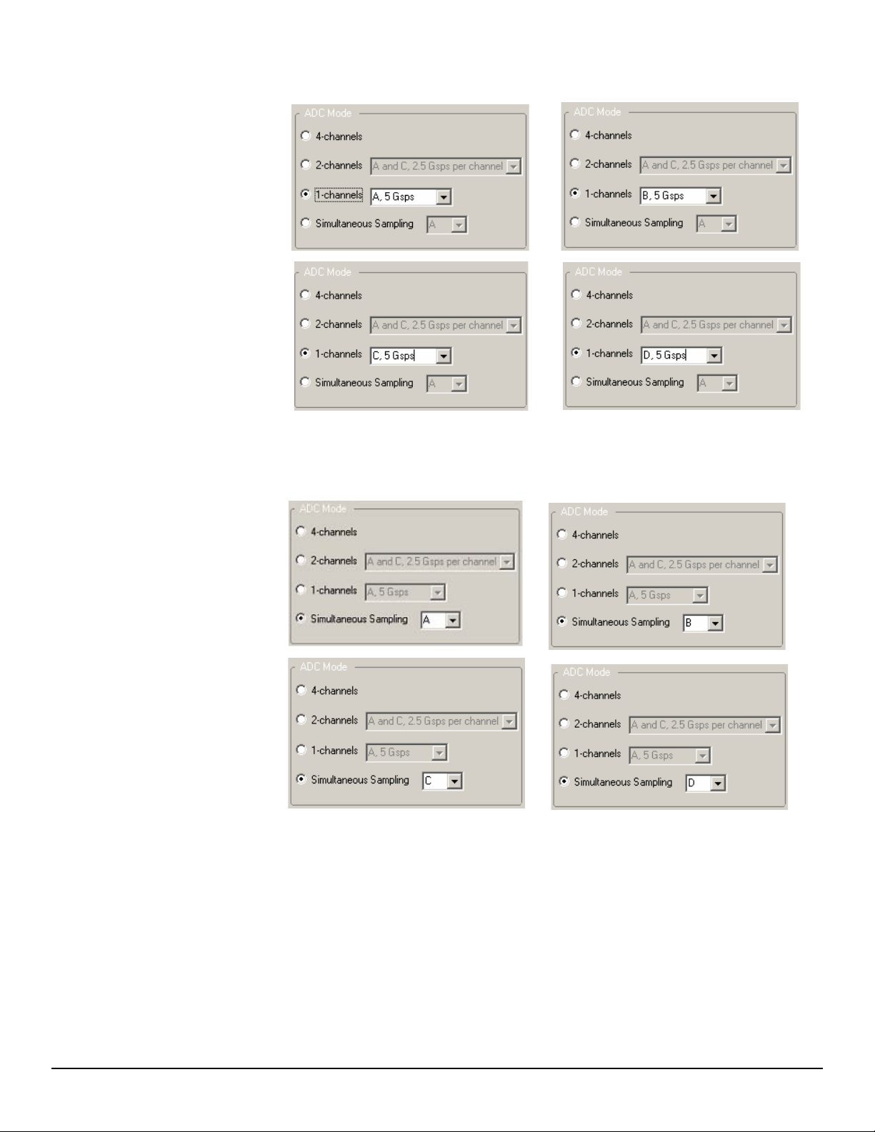
– One-channel mode = the four ADCs are all interleaved, the sampling rate is
Fclock x 2 (where Fclock is the external clock signal frequency), the analog
input can be applied to either A, B, C or D channel.
4-26 EV8AQ160-EB - User Guide
0834E–BDC–07/09
e2v semiconductors SAS 2009
Page 29
Software Tools
Figure 4-18. One channel Mode
Simultaneous sampling = all four ADCs work in 4-channel mode but with one same analog input signal which is selected as A, B, C or D
EV8AQ160-EB - User Guide 4-27
0834E–BDC–07/09
e2v semiconductors SAS 2009
Page 30
Software Tools
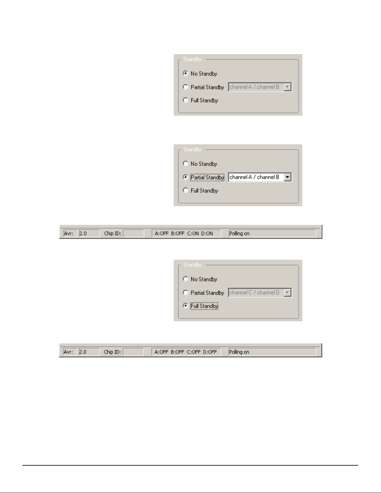
Standby mode
– No standby = all channels are active (A: ON, B: ON, C: ON, D: ON).
– Partial standby = either A and B are in standby or C and D are in standby.
– Full standby = all four ADCs are in standby.
General settings
– DMUX mode = 1:1 or 1:2 output ratio
– Output mode = Gray coding or binary coding
– Bandwidth selection = min, reduced, nominal, full band at -3 dB
– Full scale mode = either 500 mVpp or 625 mVpp
4-28 EV8AQ160-EB - User Guide
0834E–BDC–07/09
e2v semiconductors SAS 2009
Page 31
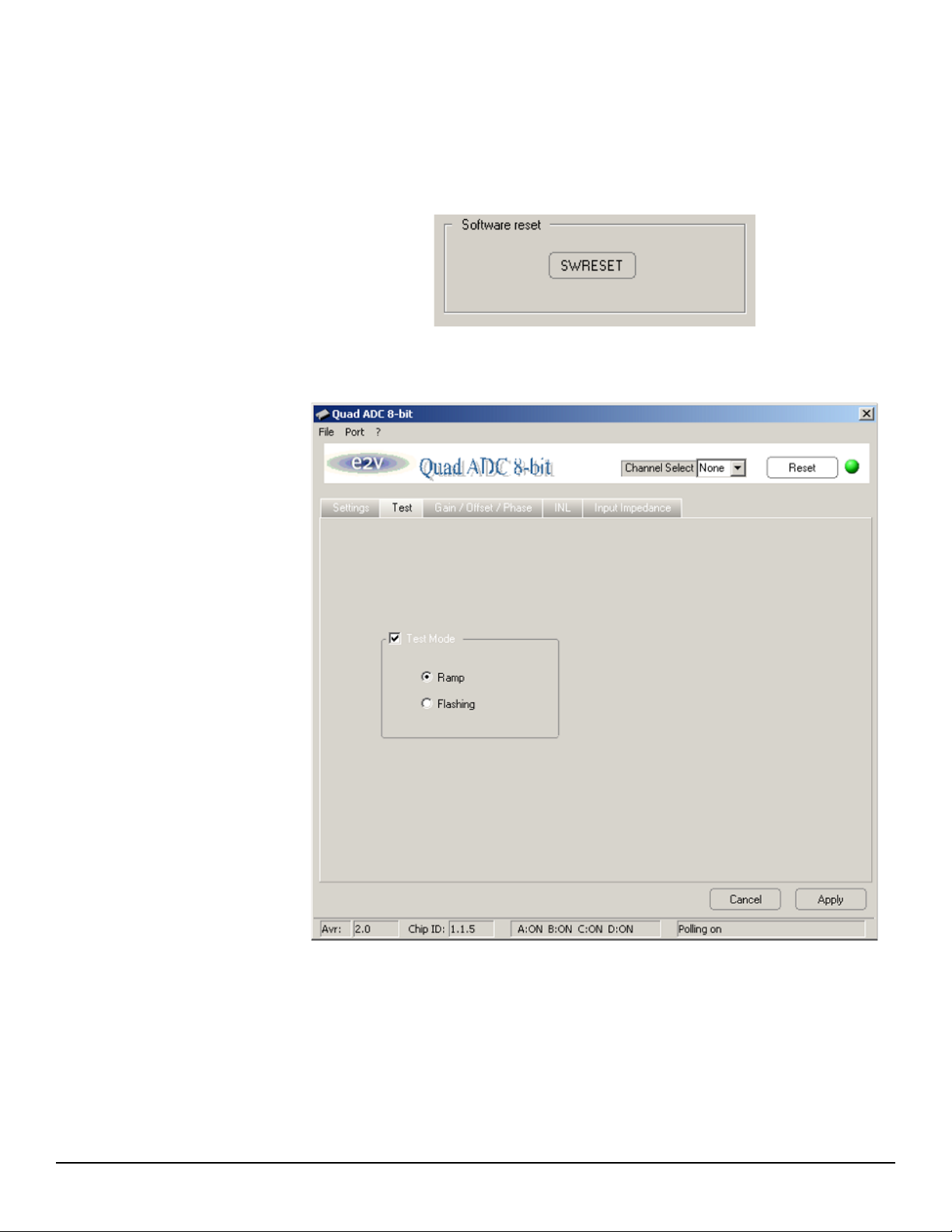
4.6.2 Test
Software Tools
Synchronization: programs the number of clock cycles prior to output clock restart
after SYNC reset
Software reset = resets the SPI by software
In this window, the test mode is available:
– Either a ramp is generated within each ADC and output
– Or a flashing bit at 1 is output on each ADC (1 FF pattern every ten 00
patterns)
EV8AQ160-EB - User Guide 4-29
0834E–BDC–07/09
e2v semiconductors SAS 2009
Page 32
Software Tools
4.6.3 Gain/Offset/Phase
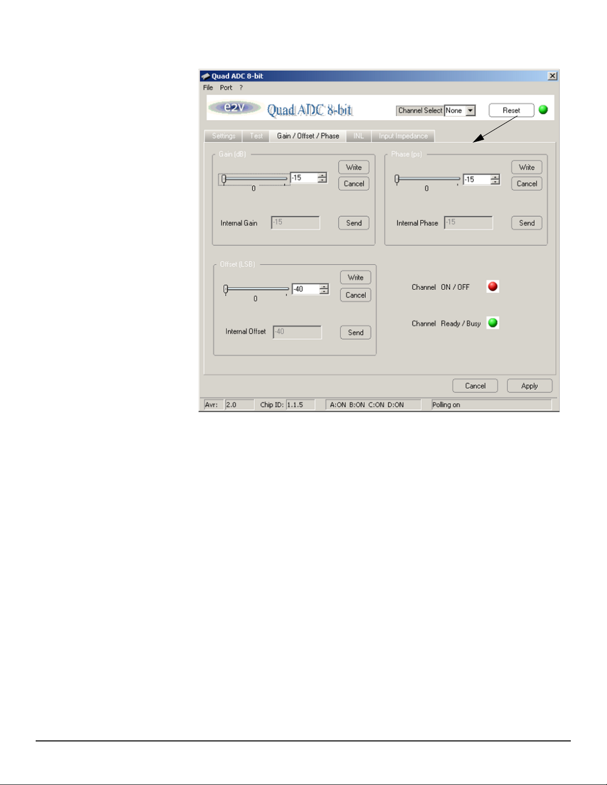
In this window, you can adjust the gain, offset and phase of the channel selected via the
channel select button on the top right of the user interface.
A LED shows if the channel is ON (active, green LED) or OFF (not active, red LED) and
if the same channel is ready (ready to receive gain, offset or phase orders, green LED)
or busy (not ready to receive new calibration orders, red LED).
Once a channel has been selected, you can adjust the gain/offset/phase of this channel:
– You first need to enter the desired value for the gain/offset/phase thanks to the
cursor.
– If you need to retrieve the old value of the gain/offset/phase click Cancel.
– Then you should write this value to the internal registers by clicking on the
Write button.
– If several adjustments are needed (gain AND offset AND phase), then select
each value and then click on the respective Write buttons.
– Once all adjustments are made via the Write buttons, then you can Send the
orders to the ADC SPI via the Send button.
– The calibration is successful if the internal gain/offset/phase boxes display the
entered values.
4-30 EV8AQ160-EB - User Guide
0834E–BDC–07/09
e2v semiconductors SAS 2009
Page 33
Software Tools
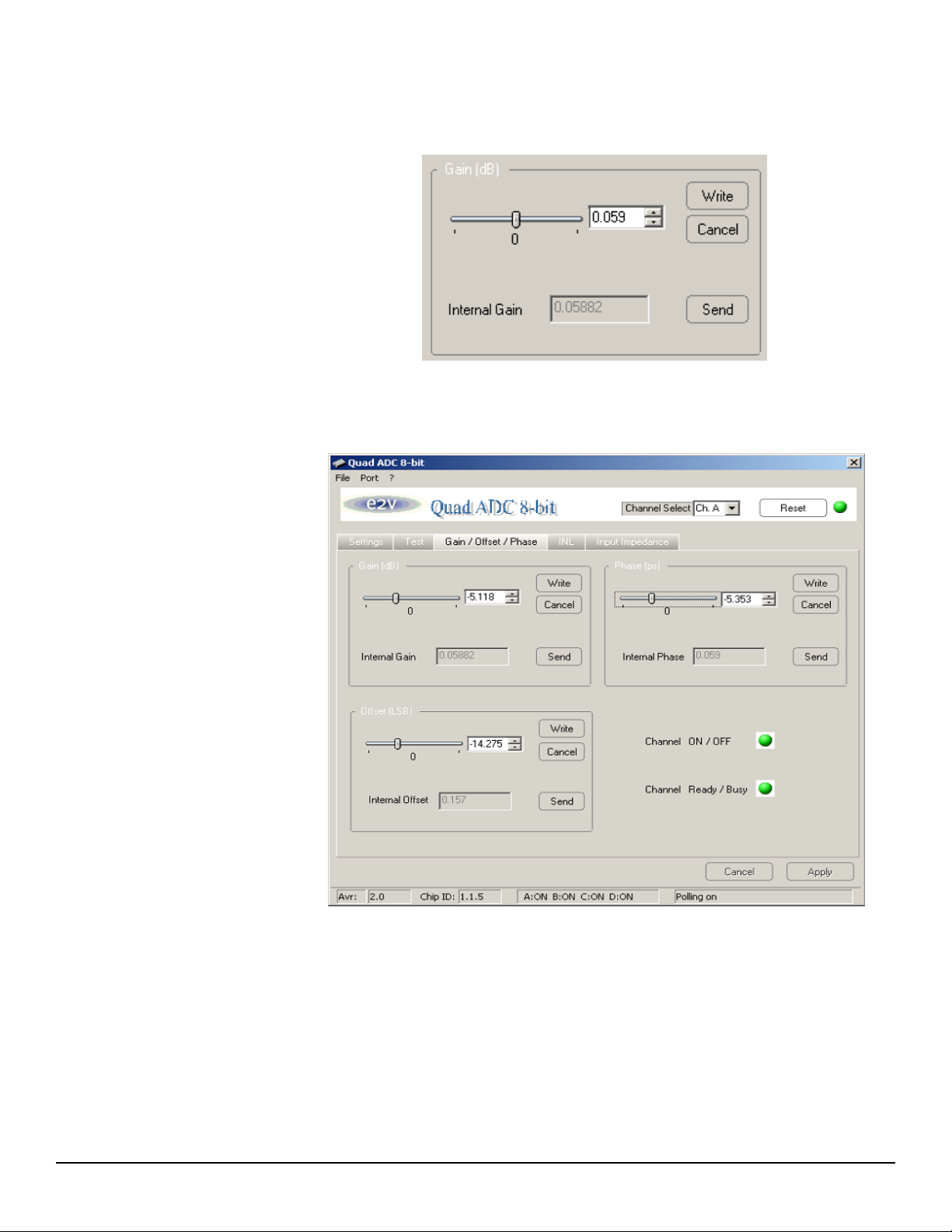
If a new value for the gain/offset/phase has been entered by mistake, it is possible to
retrieve the initial value by pushing the Cancel button.
The general Apply and Cancel buttons are not active in this window (as soon as the
Send button is pressed, the gain/offset/phase adjustments are made active).
In the following example, channel A is selected. Values for the gain, the offset and the
phase have been entered via the Write and then the Send buttons, which explains why
the Internal values are equal to the settings values.
EV8AQ160-EB - User Guide 4-31
0834E–BDC–07/09
e2v semiconductors SAS 2009
Page 34
Software Tools
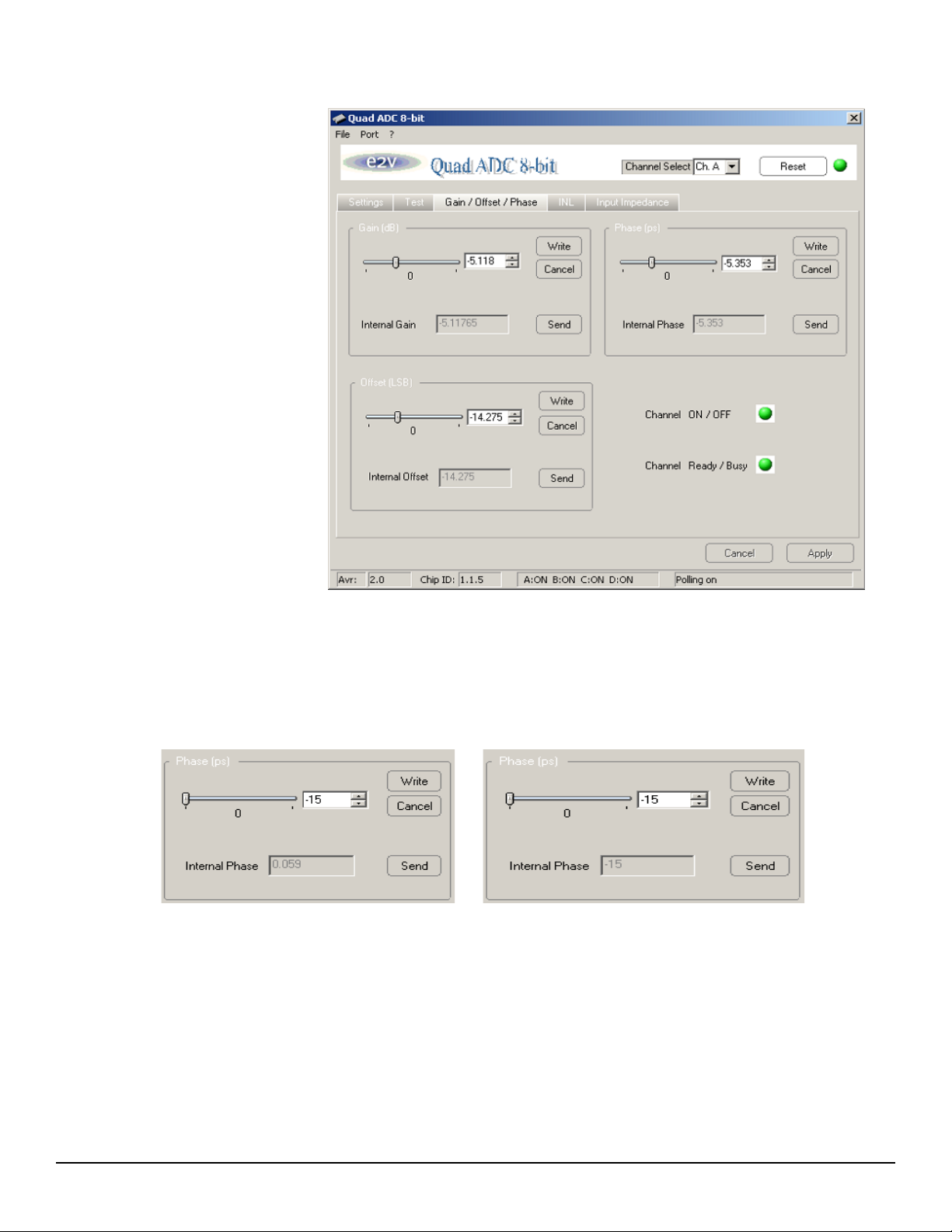
In the following example, you can see that the internal phase register is set to 0.059 and
that the user wants the phase to be set to -15 ps. In the second picture, the Write and
Send buttons have been pushed and the internal register shows the new entered value
for the phase.
4-32 EV8AQ160-EB - User Guide
0834E–BDC–07/09
e2v semiconductors SAS 2009
Page 35
4.7 INL
Software Tools
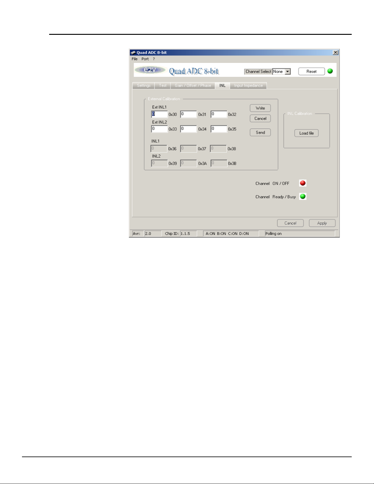
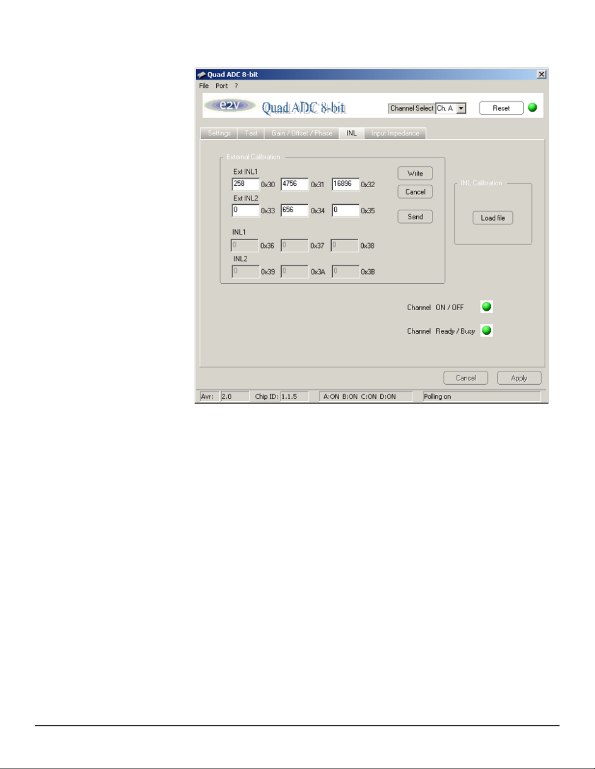
In this window, it is possible to calibrate the INL of the ADC (please refer to the specific
procedure for the INL calibration).
The process is similar to the one used for the gain/offset/phase adjustments:
– Select the channel where you need to adjust the INL
– Check that the channel is ON and READY (green LEDs)
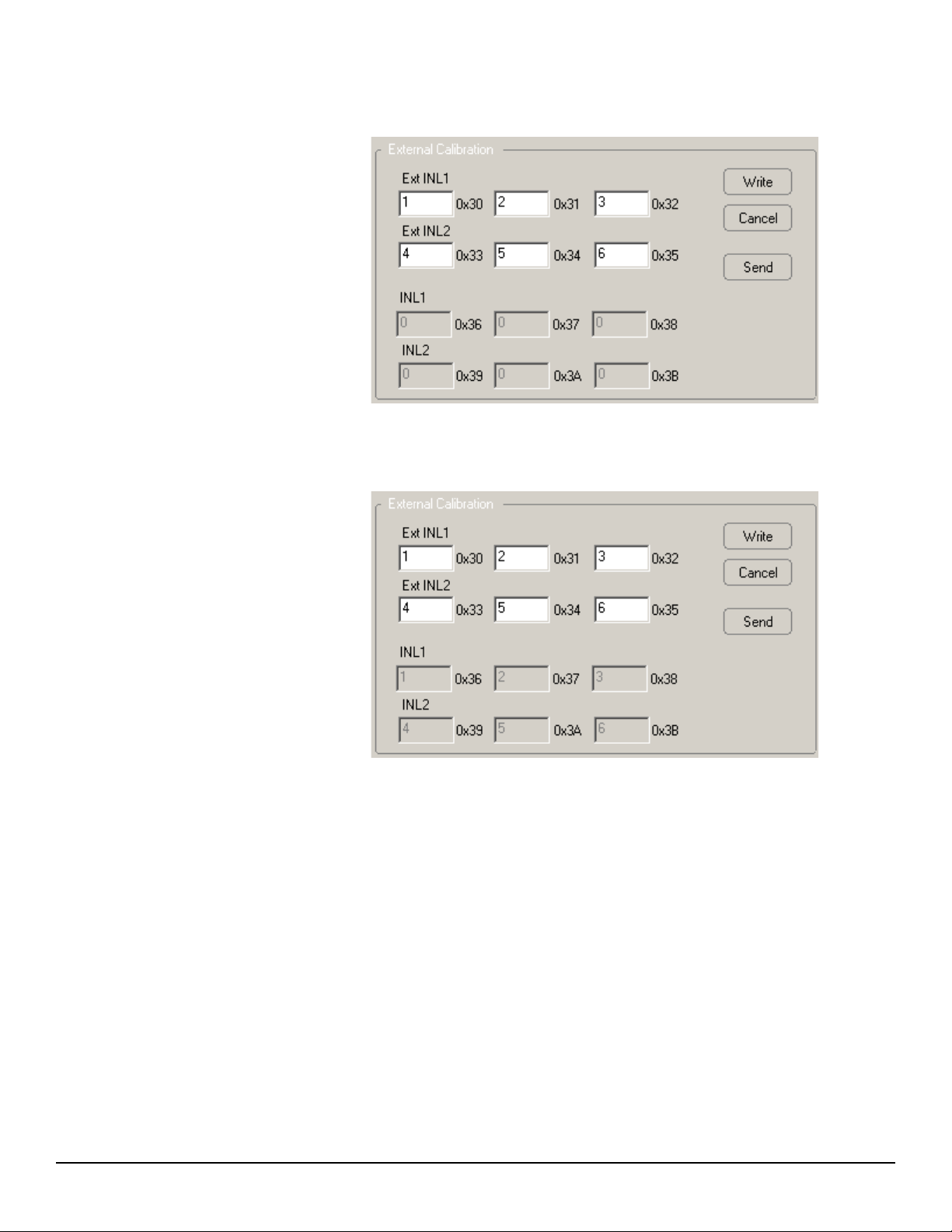
– Write the INL values in the Ext INL1 and Ext INL2 boxes
– If you need to retrieve the old value of INL click Cancel
EV8AQ160-EB - User Guide 4-33
0834E–BDC–07/09
e2v semiconductors SAS 2009
Page 36
Software Tools
– Push the Write button to write these value to the internal register.
– Push the Send to perform the calibration
4.7.1 INL Calibration Procedure
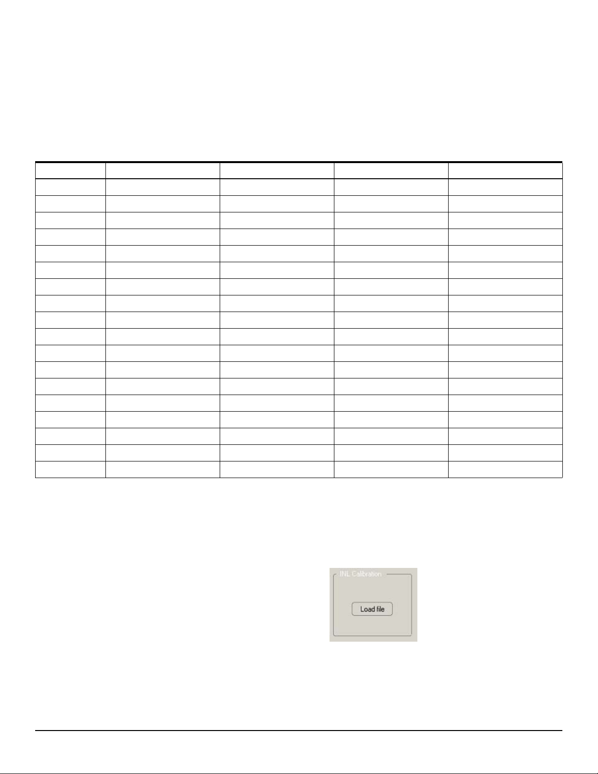
– The calibration is successful if the INL1 and INL2 boxes display the entered
values.
The calibration of the INL abides by the following rule:
If there is an INL peak (+0.5 LSB) around a specific code, then this peak can be
decreased by 0.15 LSB by writing a “1” on the bit given by the
Table 4-1 below for the
second level of correction (fifth row). If this is not sufficient to decrease the INL peak,
then you can write a “1” on the bit given by the table in the second level INL row (fourth
row). The effect will be then to decrease the INL by 0.6 LSB (the effect of rows three and
four are added).
The procedure is similar when the INL has to be increased (rows two and three).
4-34 EV8AQ160-EB - User Guide
0834E–BDC–07/09
e2v semiconductors SAS 2009
Page 37
Software Tools
Example:
The intrinsic INL obtained with the ADC has a peak (+0.5 LSB) around code 128. By
writing a “1” on bit 9 of register at address 0x34, you will be able to decrease the INL
peak. If this is not sufficient, you can write another “1” on bit 9 at address 0x31.
Table 4-1. INL Calibration Table
INL code First Level INL Second Level INL First Level INL Second Level INL
Increase by 0.45LSB Increase by 0.15 LSB Decrease by 0.45 LSB Decrease by 0.15 LSB
0 0x32 bit 8 0x35 bit 8 0x32 bit 9 0x35 bit 9
16 0x32 bit 10 0x35 bit 10 0x32 bit 11 0x35 bit 11
32 0x32 bit 12 0x35 bit 12 0x32 bit 13 0x35 bit 13
48 0x32 bit 14 0x35 bit 14 0x32 bit 15 0x35 bit 15
64 0x31 bit 0 0x34 bit 0 0x31 bit 1 0x34 bit 1
80 0x31 bit 2 0x34 bit 2 0x31 bit 3 0x34 bit 3
96 0x31 bit 4 0x34 bit 4 0x31 bit 5 0x34 bit 5
112 0x31 bit 6 0x34 bit 6 0x31 bit 7 0x34 bit 7
128 0x31 bit 8 0x34 bit 8 0x31 bit 9 0x34 bit 9
144 0x31 bit 10 0x34 bit 10 0x31 bit 11 0x34 bit 11
160 0x31 bit 12 0x34 bit 12 0x31 bit 13 0x34 bit 13
176 0x31 bit 14 0x34 bit 14 0x31 bit 15 0x34 bit 15
192 0x30 bit 0 0x33 bit 0 0x30 bit 1 0x33 bit 1
208 0x30 bit 2 0x33 bit 2 0x30 bit 3 0x33 bit 3
224 0x30 bit 4 0x33 bit 4 0x30 bit 5 0x33 bit 5
240 0x30 bit 6 0x33 bit 6 0x30 bit 7 0x33 bit 7
256 0x30 bit 8 0x33 bit 8 0x30 bit 9 0x33 bit 9
Note: Please note that the INL correction value varies as the temperature increase. 0.15 LSB is the typical correction for TJ = 50°C.
This value can vary from 0.1 LSB to 0.2 LSB from low to high temperature.
4.7.1.1 INL calibration
EV8AQ160-EB - User Guide 4-35
0834E–BDC–07/09
e2v semiconductors SAS 2009
Page 38
Software Tools
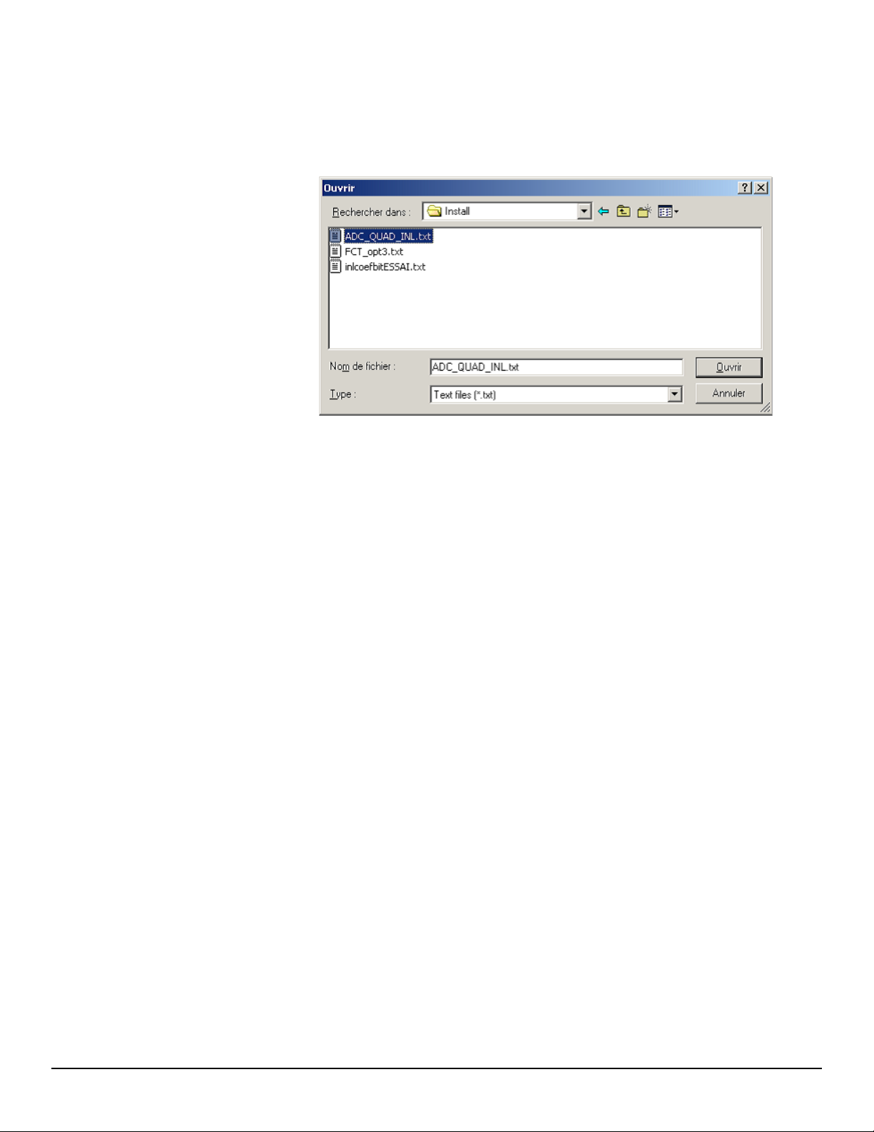
Select file
ADC_QUAD_INL.txt
This file is the INL measurement of on ADC before calibration
File txt format with 256 INL code.
4-36 EV8AQ160-EB - User Guide
0834E–BDC–07/09
e2v semiconductors SAS 2009
Page 39
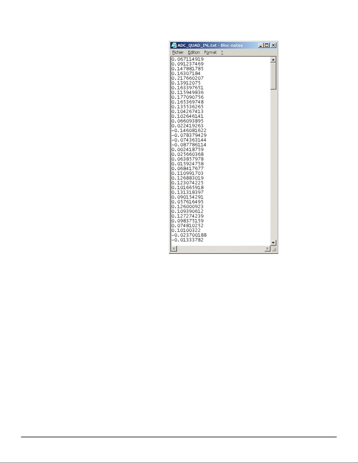
Example ADC_QUAD_INL.txt
Software Tools
After loading file, the software compute automatically the INL register
Note: Do not forget to push Write and Send button.
EV8AQ160-EB - User Guide 4-37
0834E–BDC–07/09
e2v semiconductors SAS 2009
Page 40
Software Tools
4-38 EV8AQ160-EB - User Guide
0834E–BDC–07/09
e2v semiconductors SAS 2009
Page 41
4.8 Input Impedance
Software Tools
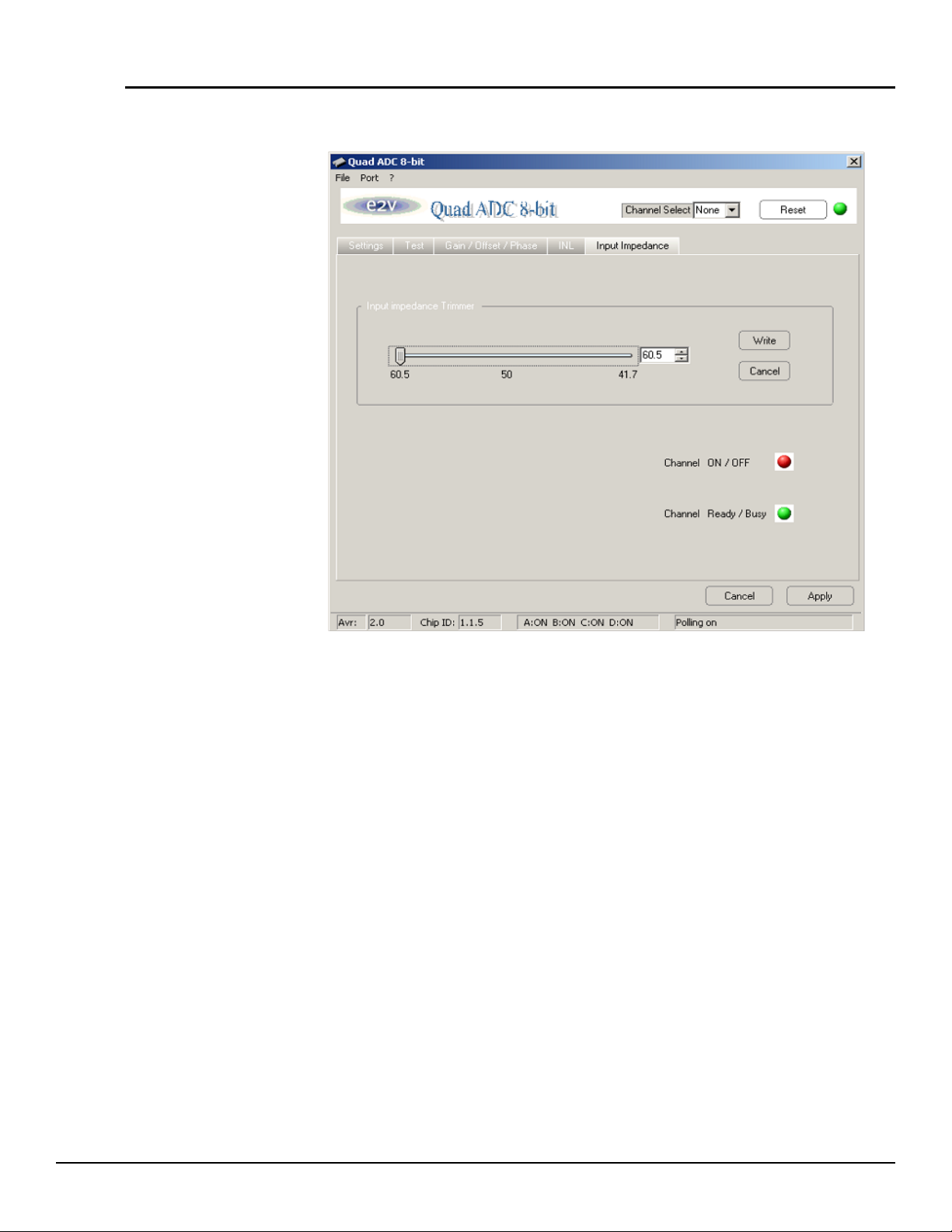
In this window, it is possible to readjust the internal input resistor, which should be
matched to 50Ω.
The procedure is similar to the previous ones:
– Select the channel where you need to adjust the input impedance
– Check that the channel is ON and READY (green LEDs)
– Enter the resistor value
– Push the Write button to write these values to the internal registers (you can
retrieve the initial value of the impedance by clicking on the Cancel button)
This function helps to readjust the input impedance in case of a slight mismatch due to
temperature variations or process variations.
EV8AQ160-EB - User Guide 4-39
0834E–BDC–07/09
e2v semiconductors SAS 2009
Page 42
Software Tools
4.9 Load and Save Configuration
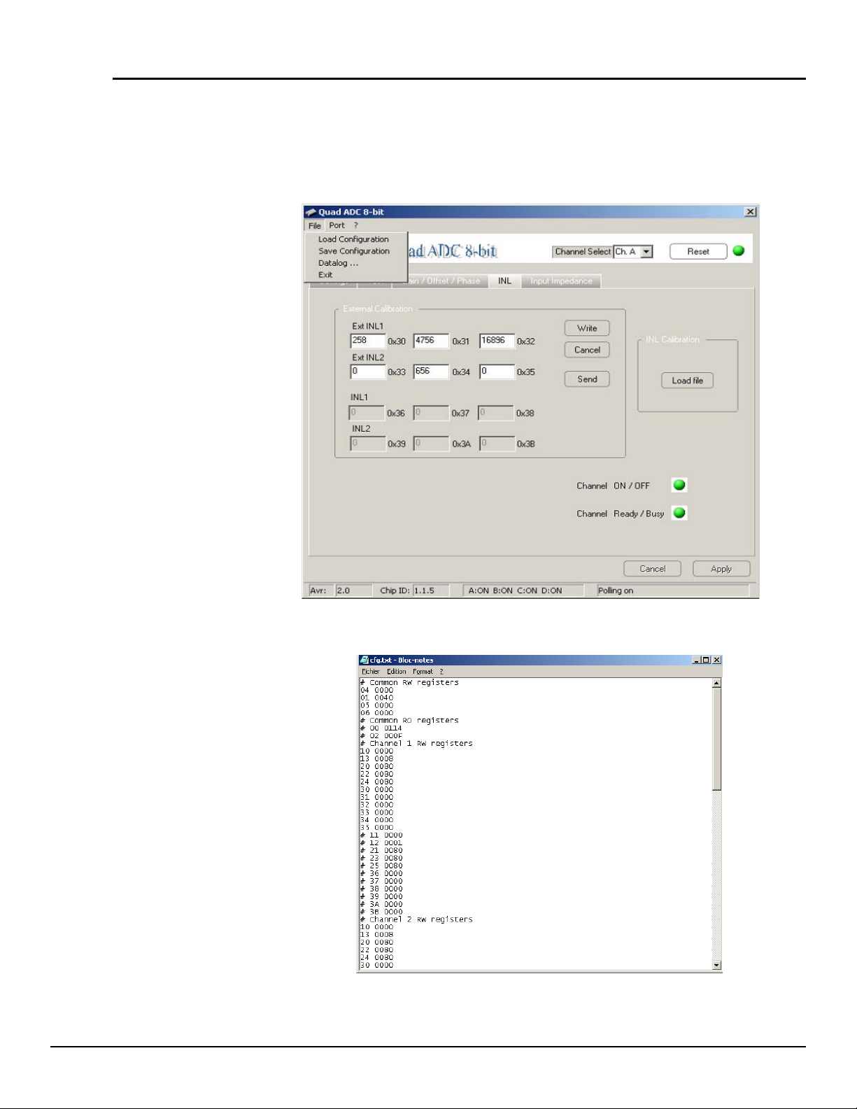
The File menu shows the possibility to load or save a configuration of the EV8AQ160 or
to create a datalog file.
It is possible to save the configuration of EV8AQ160 into a .txt file:
Select the File menu and click to Save Configuration.
Example of configuration file:
4-40 EV8AQ160-EB - User Guide
0834E–BDC–07/09
e2v semiconductors SAS 2009
Page 43
Software Tools
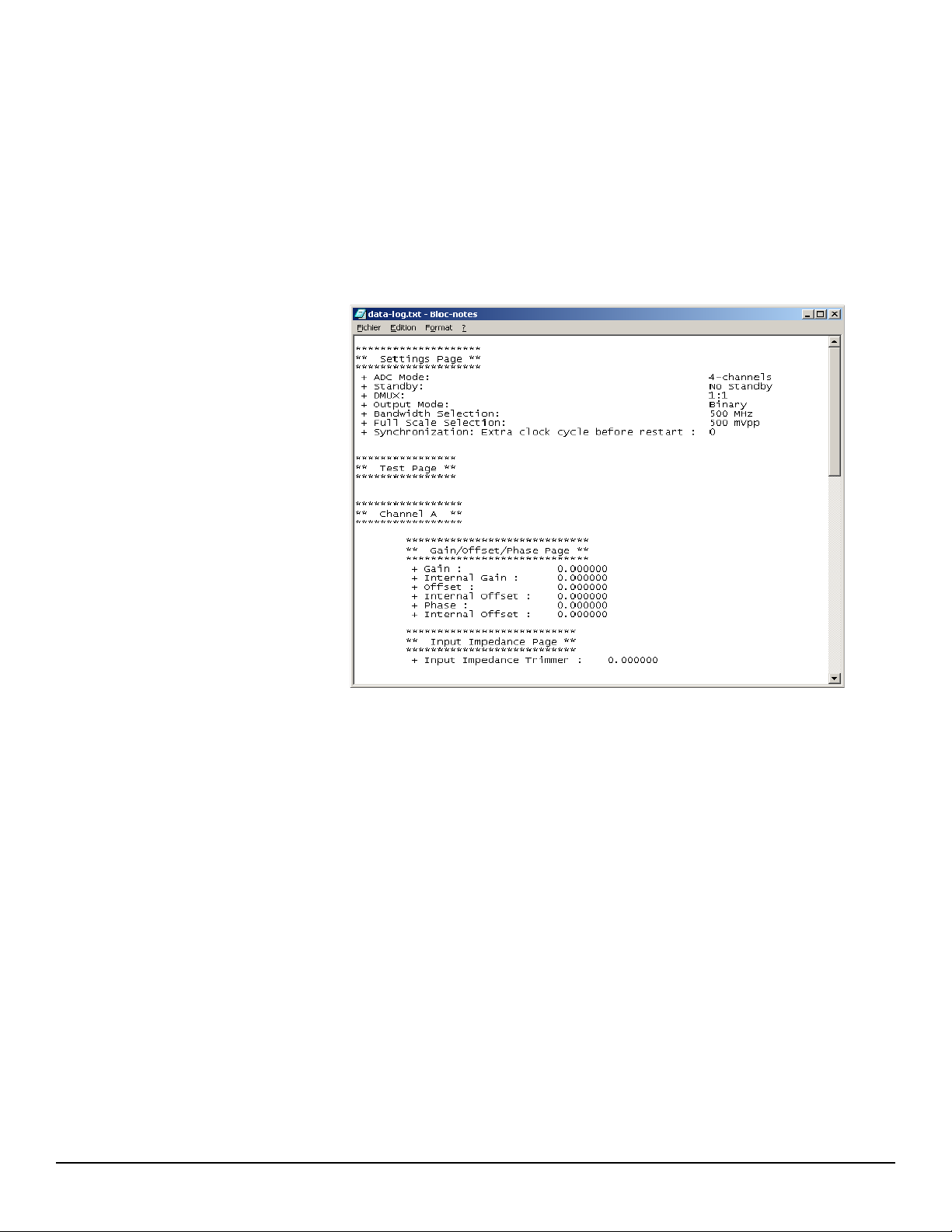
This file could be loaded into the EV8AQ160.
Select the File menu and click to Load Configuration chose the xx.txt file.
It is possible to save the Data-log of the EV8AQ160 configuration into a .txt file.
Select the File menu and click to Datalog.
Example of Datalog file:
EV8AQ160-EB - User Guide 4-41
0834E–BDC–07/09
e2v semiconductors SAS 2009
Page 44

Software Tools
4-42 EV8AQ160-EB - User Guide
0834E–BDC–07/09
e2v semiconductors SAS 2009
Page 45
Section 5
Application Information
5.1 Analog Input The analog input (XAI, XAIN) are entered in differential AC coupled mode as described
in
Figure 5-1.
The single-ended operation for the analog input is allowed but it may degrade the ADC
performance significantly. It is thus recommended to use a differential source to drive
the analog inputs of this ADC (external balun or differential amplifier).
Note: For characterization purposes, we used the following transformers:
Table 5-1. Transformers Details
Frequency
Part Number Supplier
H9 MACOM 2 MHz 2GHz Analog/Clock SMA
3A0056 ANAREN 2 GHz 4GHz Analog/Clock SMA
4020080 KRYTAR 2 GHz 8GHz Analog/Clock SMA
In order to optimize the performance of the ADC, it is also recommended to use a band
pass filter on the analog input path.
Range Signal
Connector
Typ e
EV8AQ160-EB - User Guide 5-43
0834E–BDC–07/09
e2v semiconductors SAS 2009
Page 46
Application Information
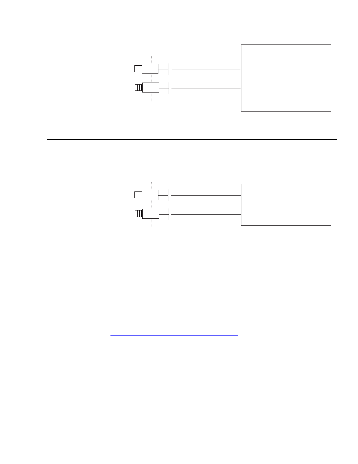
Figure 5-1. Differential Analog or Clock Inputs Implementation
10 nF
XAI or
CLK
XAI or CLK
EV8AQ160
XAIN or
CLKN
10 nF
XAIN or CLKN
5.2 Clock Input The clock input can be entered indifferently in single-ended or differential mode with no
performance degradation. The clock is AC coupled via 10 nF capacitors as described in
Figure 5-2.
Figure 5-2. Clock Input Implementation
10 nF
CLKI
CLKI (H1)
EV8AQ160
CLKIN
10 nF
If used in single-ended mode, CLKIN should be terminated to ground via a 50Ω resistor.
This is physically done by shorting the SMA on CLKIN with a 50Ω cap.
CLKIN (J1)
The jitter performance on the clock is crucial to obtain optimum performance from the
ADC. We thus recommend to use a very low phase noise clock and to filter the clock
signal if a fixed frequency is used.
For a clock at 500 MHz, we use in our testbench:
Pass band filter from LORCH MICROWAVE 9BP8-500/30-S (up to 8 dB attenuation,
70 dB rejection up to 5000 MHz)
500-14512 500 MHz-SC Sprinter Crystal Oscillator from WENZEL Associates
For 2.5 GHz external clock source, we suggest:
http://www.vectron.com/products/xo/co-287w.htm
or Crystek CPLL66-240-2500
5-44 EV8AQ160-EB - User Guide
0834E–BDC–07/09
e2v semiconductors SAS 2009
Page 47
5.3 RESET input The Syncp, Syncn is necessary to start the ADC after power up.
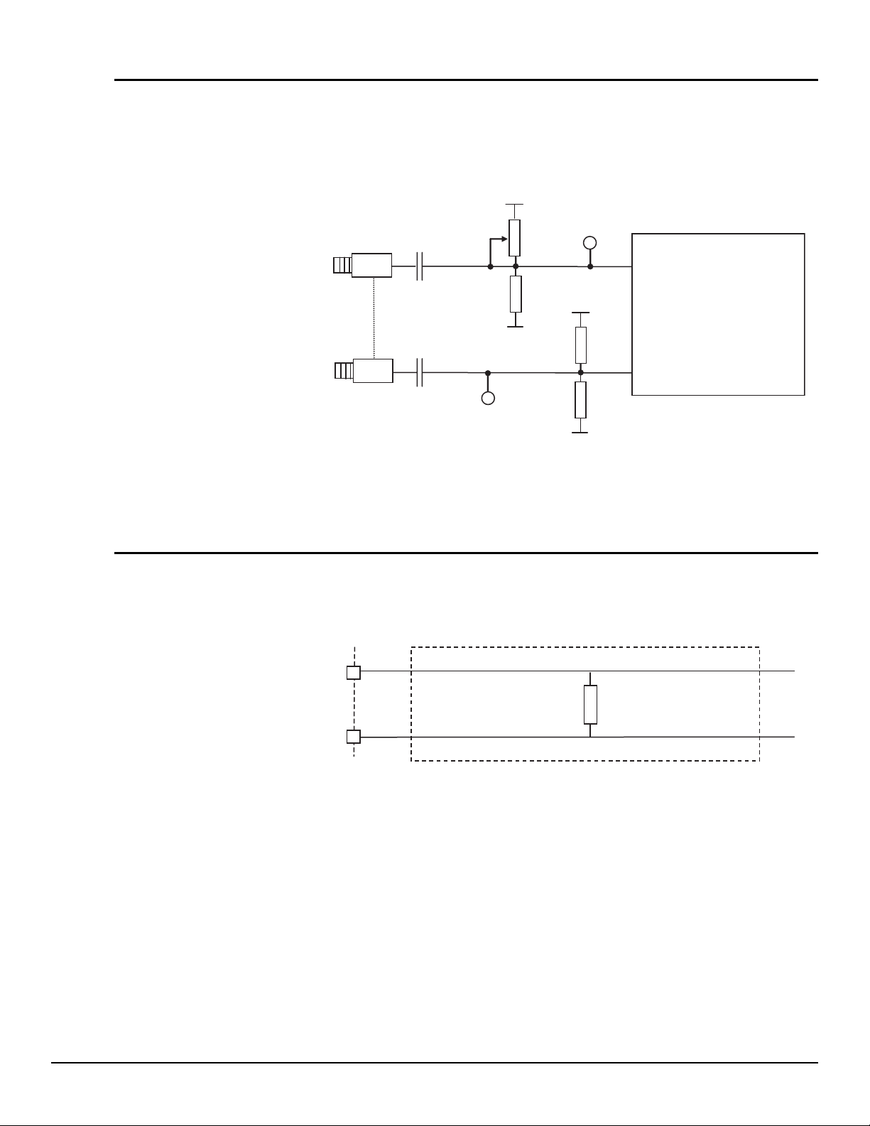
The reset signal is implemented as illustrated in Figure 5-3.
Figure 5-3. SYNC, SYNCN Inputs Implementation
3.3V
Test Point
GND
500Ω
SYNC (AC11)
200Ω
3.3V
200Ω
SYNC
SMA
10 nF
Application Information
AQEV8 160
SYNCN
SMA
10 nF
200Ω
Test Point
GND
SYNCN (AD11)
The resistors are used only for pull up and down of the SYNC signals. For reset, apply a
pulse signal with a pulse generator via the SYNC SMA or apply directly a DC voltage
(0.9V-1.3V) via the test points
5.4 Output Data The output data are LVDS and are 100Ω terminated to ground as shown in Figure 5-4.
Figure 5-4. Output Data on-board Implementation
Connector
100
Ω
ADC
The data are output in binary format and in double data rate (the output clock frequency
is half the data rate and thus half the input clock frequency).
EV8AQ160-EB - User Guide 5-45
0834E–BDC–07/09
e2v semiconductors SAS 2009
Page 48
Application Information
5.5 CMIRefAB and CMIRefCD Output Signals
5.6 Diode for Junction Temperature Monitoring
Two 2 mm banana jacks are provided for the CMIRefAB and CMIRefCD signals which
provides the analog input common mode voltages (= 1.8V).
As the analog input is entered in AC coupled mode, these CMIRefAB and CMIRefCD
signals do not need to be used.
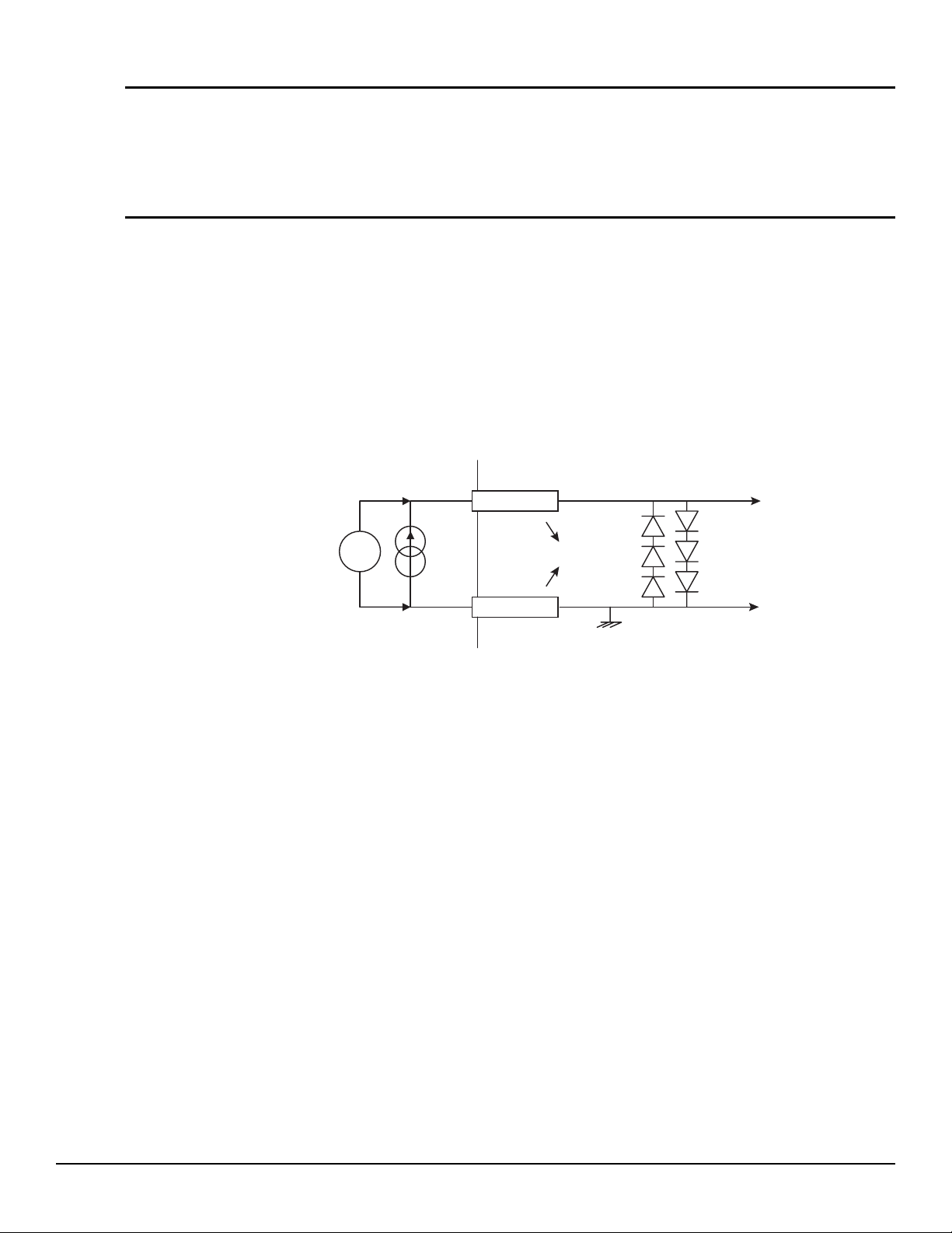
Two 2 mm banana jacks are provided for the die junction temperature monitoring of the
ADC.
One banana jack is labeled DIODA and should be applied a current of up to 1 mA (via a
multimeter used in current source mode) and the second one is connected to DIODC.
The ADC diode is protected via 2 x 3 head-to-tail diodes.
Figure 5-5 describes the setup for the die junction temperature monitoring using a
multimeter.
Figure 5-5. Die Temperature Monitoring Test Setup
DIODA
V
1 mA
Banana
Jacks
Protection Diodes
To DIODA
DIODC
To DIODC
5-46 EV8AQ160-EB - User Guide
0834E–BDC–07/09
e2v semiconductors SAS 2009
Page 49
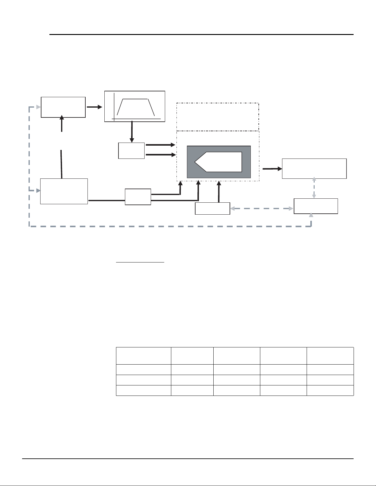
5.7 Test Bench Description
Figure 5-6. Test Bench Description
Band pass filter
Filter
Application Information
Input Signal
Generator
10 MHz
synchronisation
Clock Signal
Generator
Thermal system
Temperature range
-80 to +163˚
Balun
AAIN
AAI
Evaluation Board
Quad ADC
8-bit
CLKINCLKI
Balun
Supply
GPIB
Signal Generator:
Agilent E4426B 250 KHz 4 GHz (High spectral purity)
Digital Acquisition
System
Computer
HP8665B 0.1 6000MHz opt 001 004 (High spectral purity)
Marconi Instrument 2042 10 kHz-5.4 GHz
SMA100A 9 KHz 6 GHz (High spectral purity)
All measurements should be performed in differential configuration for analog and clock
input. The following baluns could be used:
Frequency
Part Number Supplier
H9 MACOM 2 MHz 2 GHz Analog/Clock SMA
3A0056 ANAREN 2 GHz 4 GHz Analog/Clock SMA
4020080 KRYTAR 2 GHz 8 GHz Analog/Clock SMA
EV8AQ160-EB - User Guide 5-47
Range
Signal
Connector
Typ e
0834E–BDC–07/09
e2v semiconductors SAS 2009
Page 50

Application Information
5-48 EV8AQ160-EB - User Guide
0834E–BDC–07/09
e2v semiconductors SAS 2009
Page 51
Section 6
Ordering Information
6.1 Ordering Information
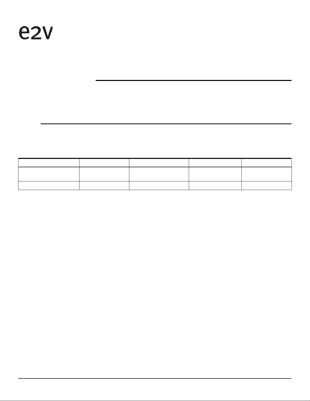
Table 6-1. Ordering Information
Part Number Package Temperature Range Screening Level Comments
Commercial C grade
EV8AQ160CTPY EBGA 380 RoHS
EV8AQ160TPY-EB EBGA 380 RoHS Ambient Prototype Evaluation board
0°C < T
< 70°C Standard
amb
EV8AQ160-EB - User Guide 6-47
0834E–BDC–07/09
e2v semiconductors SAS 2009
Page 52

Ordering Information
6-48 EV8AQ160-EB - User Guide
0834E–BDC–07/09
e2v semiconductors SAS 2009
Page 53
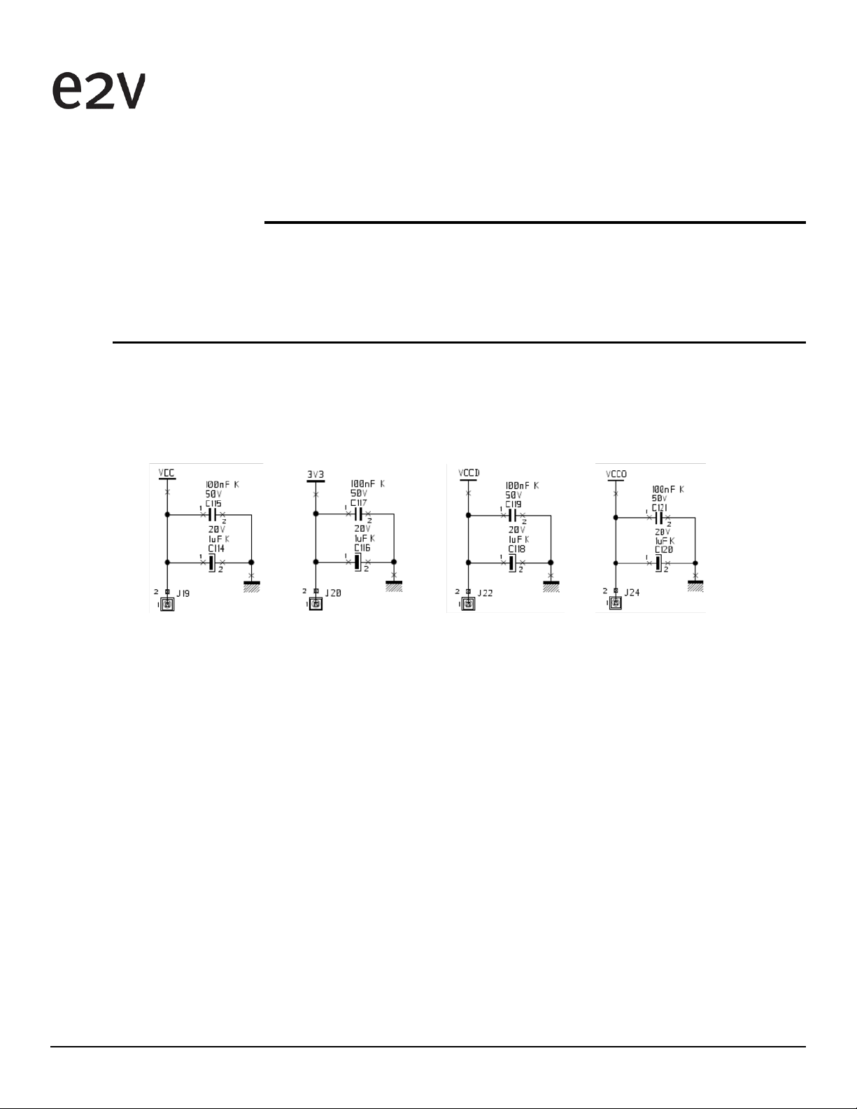
7.1 EV8AQ160-EB Electrical Schematics
Figure 7-1. Power Supplies Bypassing
Section 7
Appendices
EV8AQ160-EB - User Guide 7-49
0834E–BDC–07/09
e2v semiconductors SAS 2009
Page 54
Appendices
Figure 7-2. Power Supplies Decoupling (J = ± 5% Tolerance)
7-50 EV8AQ160-EB - User Guide
0834E–BDC–07/09
e2v semiconductors SAS 2009
Page 55
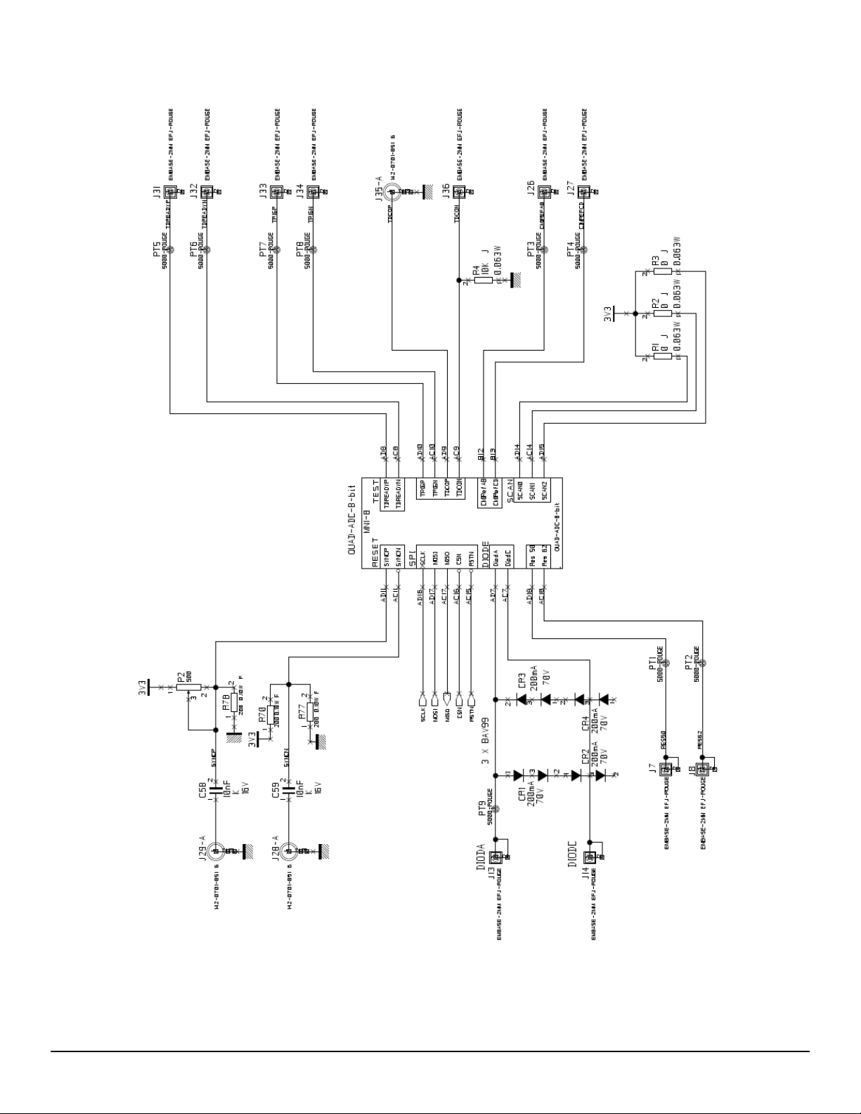
Figure 7-3. Electrical Schematics (ADC)
Appendices
EV8AQ160-EB - User Guide 7-51
0834E–BDC–07/09
e2v semiconductors SAS 2009
Page 56
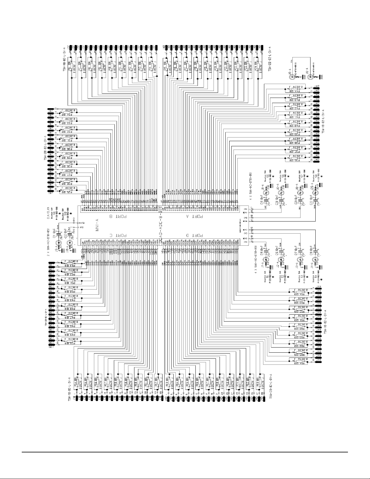
Appendices
Figure 7-4. Electrical Schematics (ADC)
7-52 EV8AQ160-EB - User Guide
0834E–BDC–07/09
e2v semiconductors SAS 2009
Page 57
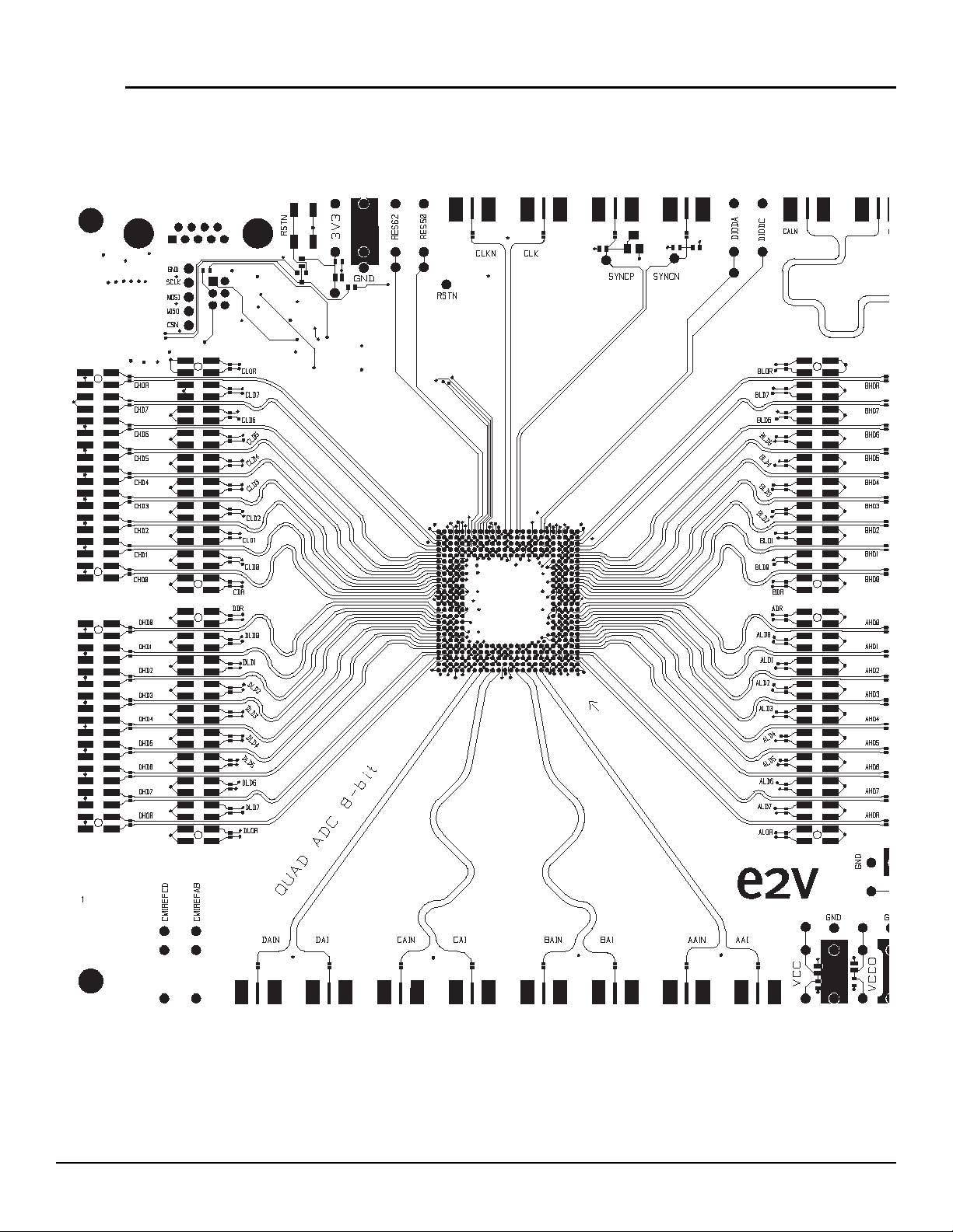
7.2 EV8AQ160-EB Board Layers
Figure 7-5. Top Layer
Appendices
EV8AQ160-EB - User Guide 7-53
0834E–BDC–07/09
e2v semiconductors SAS 2009
Page 58
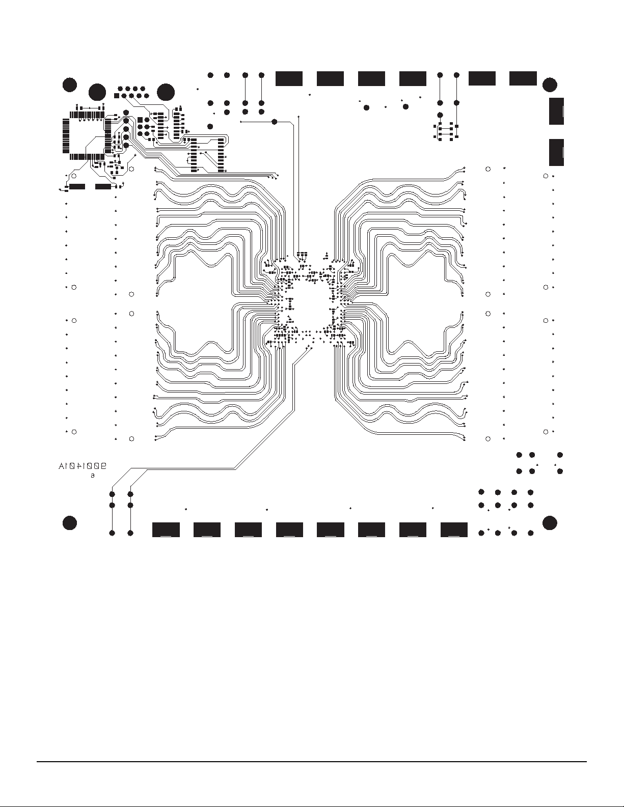
Appendices
Figure 7-6. Bottom Layer
7-54 EV8AQ160-EB - User Guide
0834E–BDC–07/09
e2v semiconductors SAS 2009
Page 59
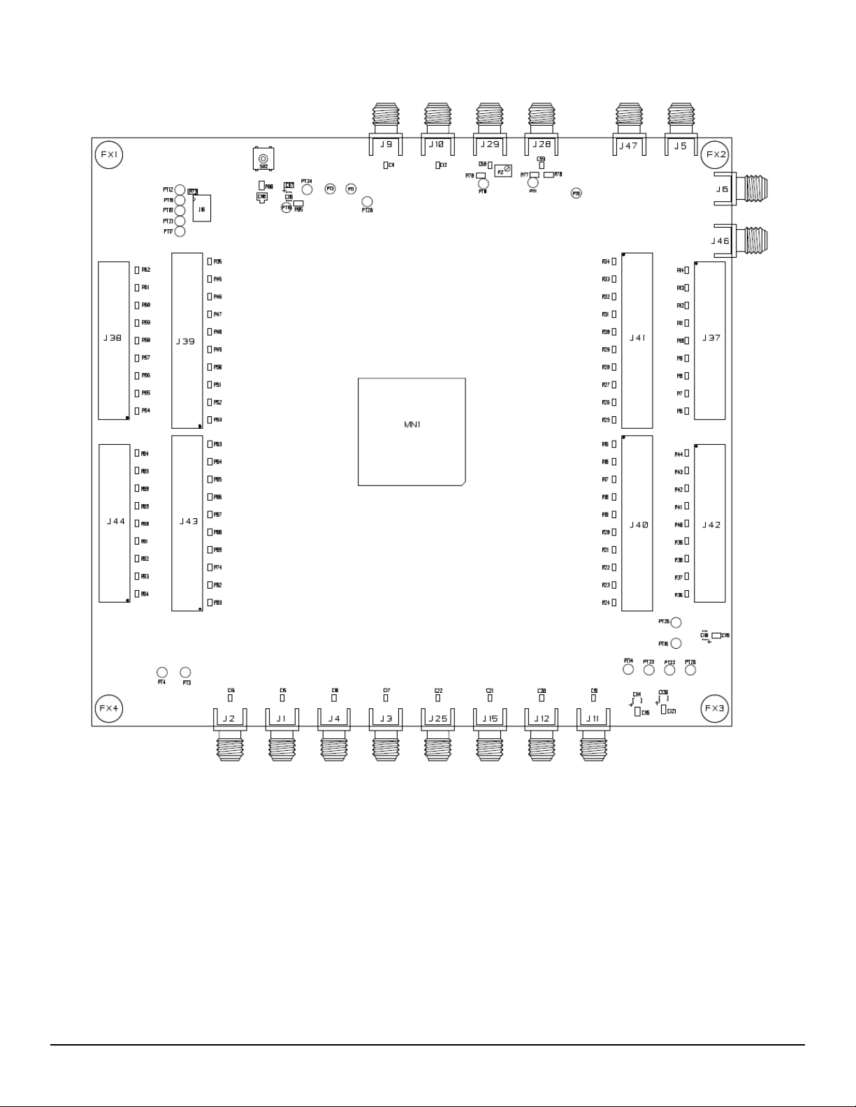
Figure 7-7. Equipped Board (Top)
Appendices
EV8AQ160-EB - User Guide 7-55
0834E–BDC–07/09
e2v semiconductors SAS 2009
Page 60
Appendices
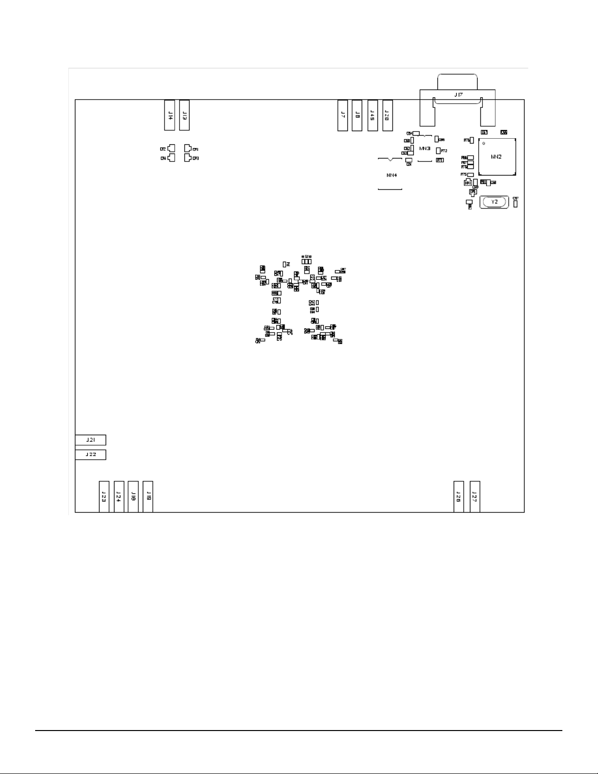
Figure 7-8. Equipped Board (Bottom)
7-56 EV8AQ160-EB - User Guide
0834E–BDC–07/09
e2v semiconductors SAS 2009
Page 61

How to reach us
Home page: www.e2v.com
Sales offices:
Europe Regional sales office
e2v ltd
106 Waterhouse Lane
Chelmsford Essex CM1 2QU
England
Tel: +44 (0)1245 493493
Fax: +44 (0)1245 492492
mailto: [email protected]
e2v sas
16 Burospace
F-91572 Bièvres Cedex
France
Tel: +33 (0) 16019 5500
Fax: +33 (0) 16019 5529
mailto: [email protected]
e2v gmbh
Industriestraße 29
82194 Gröbenzell
Germany
Tel: +49 (0) 8142 41057-0
Fax: +49 (0) 8142 284547
mailto: [email protected]
Americas
e2v inc
520 White Plains Road
Suite 450 Tarrytown, NY 10591
USA
Tel: +1 (914) 592 6050 or 1-800-342-5338,
Fax: +1 (914) 592-5148
mailto: [email protected]
Asia Pacific
e2v ltd
11/F.,
Onfem Tower,
29 Wyndham Street,
Central, Hong Kong
Tel: +852 3679 364 8/9
Fax: +852 3583 1084
mailto: [email protected]
Product Contact:
e2v
Avenue de Rochepleine
BP 123 - 38521 Saint-Egrève Cedex
France
Tel: +33 (0)4 76 58 30 00
Hotline:
mailto: [email protected]
Whilst e2v has taken care to ensure the accuracy of the information contained herein it accepts no responsibility for the consequences of any
use thereof and also reserves the right to change the specification of goods without notice. e2v accepts no liability beyond that set out in its standard conditions of sale in respect of infringement of third party patents arising from the use of tubes or other devices in accordance with information contained herein.
e2v semiconductors SAS 2009
0834E–BDC–07/09
Page 62

vi
0834E–BDC–07/09
e2v semiconductors SAS 2007
 Loading...