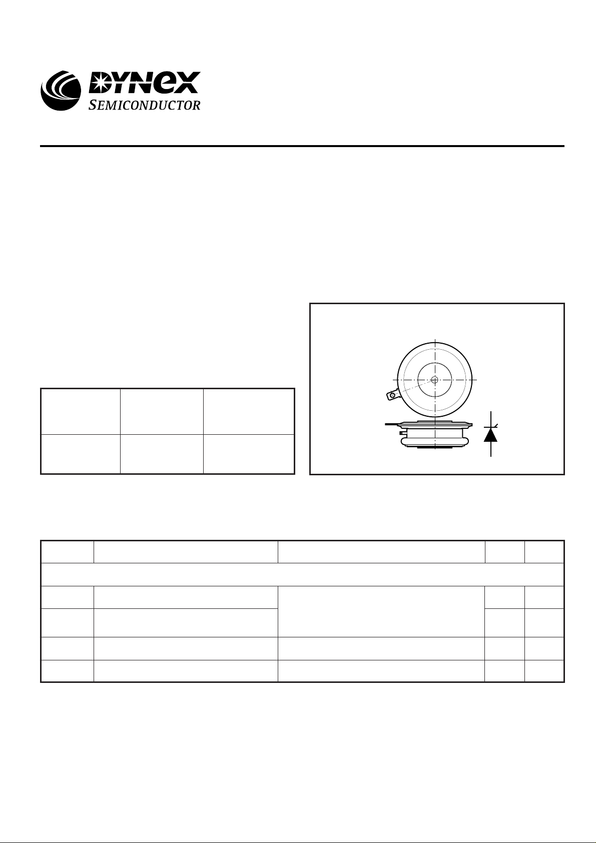
DYNEX TA44914W, TA44910W, TA44912W Datasheet

TA449..W
TA449..W
Asymmetric Thyristor
Advance Information
Replaces March 1998 version, DS4681-4.1 DS4681-5.0 January 2000
APPLICATIONS
■ UPS
■ Induction Heating
■ A.C. Motor Drives
■ Switch Mode Power Supplies
■ Choppers
FEATURES
■ Low Loss Asymmetrical Diffusion Structure
■ Fully Characterised For Operation up to 20kHz
■ High dI/dt and dV/dt ratings
VOLTAGE RATINGS
Type Number Repetitive Peak
Off-state Voltage
V
DRM
V
TA449 14 W
TA449 12 W
TA449 10 W
1400
1200
1000
Repetitive Peak
Reverse Voltage
V
RRM
V
10
10
10
KEY PARAMETERS
V
DRM
I
T(RMS)
I
TSM
dVdt 1000V/
1400V
400A
4000A
µs
dI/dt 1000A/µs
t
q
10.0µs
Lower voltage grades available.
See Package Details for further information.
CURRENT AND SURGE RATINGS
Symbol Parameter Conditions
Double Side Cooled
I
T(AV)
I
T(RMS)
I
TSM
I
2
t
Mean on-state current 255 A
RMS value
Surge (non-repetitive) on-state current
2
t for fusing
I
Half sine wave, duty cycle 50%,
= 80oC, Tj = 125˚C.
T
case
Tj = 125oC, tp = 1ms, VR = 0 4000 A
t
≥ 10ms 80 x 10
p
Outline type code: MU86.
UnitsMax.
400 A
3
A2s
1/12

TA449..W
THERMAL AND MECHANICAL DATA
Symbol Parameter
R
th(j-c)
th(c-h)
T
T
vj
stg
-
Thermal resistance - junction to case
Thermal resistance - case to heatsinkR
Virtual junction temperature
Storage temperature range
Clamping force
DYNAMIC CHARACTERISTICS
ParameterSymbol Conditions
Conditions Min. Max. Units
Double side cooled
dc
- 0.07
Single side cooled
- 0.154
0.02
-
- 0.04
Clamping force 5.0kN
with mounting compound
Cathode dc
Double side
Single side
On-state (conducting) - 135
Reverse (blocking)
-
125
-40 150
4.5 5.5 kN
Typ. Max. Units
o
C/W
o
C/W- 0.133Anode dc
o
C/W
o
C/W
o
C/W
o
o
o
C
C
C
V
I
I
TM
RRM
DRM
Maximum on-state voltage At 600A peak, T
Peak reverse current At V
Off-state current At V
RRM
DRM
dV/dt Maximum linear rate of rise of off-state voltage To 60% V
Rate of rise of on-state currentdI/dt
Gate source 20V, 20Ω
tr ≤ 5µs.
I
H
I
L
t
q
Holding current Tj = 25oC, ITM = 1A, VD = 12V - 80 mA
Latching current Tj = 25oC, IG = 0.5A, VD = 12V - 300 mA
Max. turn-off time VR = DF451 voltage drop,
Tj = 125oC, ITM = 200A,
dV/dt = 400V/µs (linear to 60% V
tdIR/dt = 30A/µs Gate open.
t
gt
t
gd
Typ. turn-on time (total)
Typ. delay time -1.5 µs
= 25oC, IT = 50A,
T
j
VD = 300V, IG = 1A, dI/dt = 50A/µs,
dIG/dt = 1A/µs
= 125oC
case
, T
= 125oC
case
, T
= 125oC-1mA
case
= 125oC, Gate open circuit
DRM Tj
Non-repetitive
- 2.9 V
-40mA
- 1000 V/µs
- 1000 A/µs
- 500 A/µsRepetitive
10- µs
),
DRM
-3 µs
2/12

GATE TRIGGER CHARACTERISTICS AND RATINGS
TA449..W
V
V
V
I
P
GT
I
GT
GD
RGM
FGM
GM
G(AV)
ConditionsParameterSymbol
Gate trigger voltage V
Gate trigger current
Min. non trigger voltage -0.2 V
Peak reverse gate voltage
= 12V, RL = 3Ω, T
DWM
V
= 12V, RL = 3Ω, T
DWM
= 25oC
case
= 25oC
case
-
-
Min.
Peak forward gate current -
Peak gate power Average gate power
Average time 10ms maxP
Max. Units
-5V
- 400 mA
-5V
-4A
-16W
-3W
3/12

TA449..W
CURVES
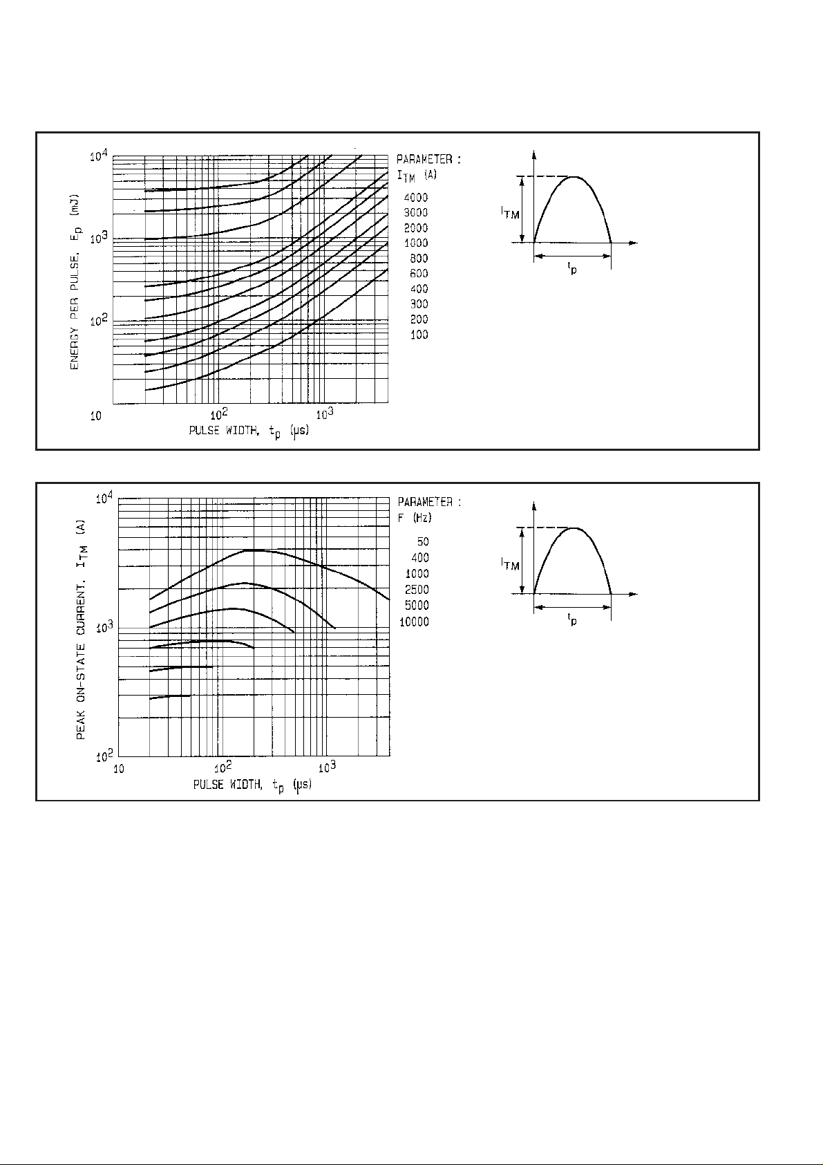
Fig.1 Energy per pulse for sinusoidal pulses.
Notes:
1. VD ≤ 600V.
≤ 1V.
2. V
R
3. R.C. snubber. C = 0.22µF, R = 4.7Ω.
4. Double side cooled.
4/12
Notes:
1. VD ≤ 600V.
= 1V.
2. V
R
3. R.C. snubber. C = 0.22µF, R = 4.7Ω.
4. Double side cooled.
Fig.2 Maximum allowable peak on-state current vs pulse width for T
case
= 65˚C.
 Loading...