

Page 1
查询DS1112SG供应商
DS2907SA
DS2907SA
Rectifier Diode
DS5740-1.0 February 2004
FEATURES
■ Double Side Cooling
■ High Surge Capability
APPLICATIONS
■ Rectification
■ Freewheel Diode
■ DC Motor Control
■ Power Supplies
VOLTAGE RATINGS
Type Number Repetitive Peak
Reverse Voltage
V
RRM
V
DS2907SA52
DS2907SA50
DS2907SA48
DS2907SA46
DS2907SA44
Lower voltage grades available
5200
5000
4800
4600
4400
Conditions
= V
V
RSM
RRM
+ 100V
KEY PARAMETERS
V
5200V
RRM
I
4914A
F(AV)
I
70000A
FSM
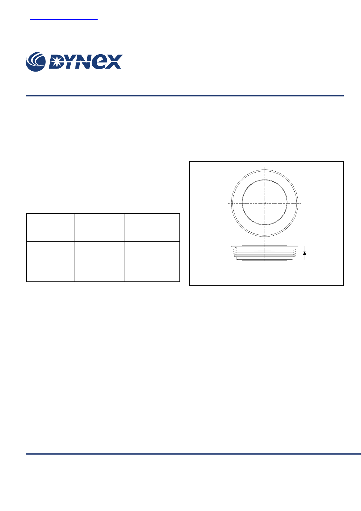
Outline type code: A
See Package Details for further information.
Fig. 1 Package outline
ORDERING INFORMATION
When ordering, select the required part number shown in the
Voltage Ratings selection table, e.g.:
DS2907SA48
Note: Please use the complete part number when ordering
and quote this number in any future correspondance relating
to your order.
www.dynexsemi.com
1/7
Page 2
DS2907SA
CURRENT RATINGS
T
= 75oC unless otherwise stated
case
Symbol Parameter Conditions
Double Side Cooled
I
F(AV)
I
F(RMS)
I
Mean forward current
RMS value
F
Continuous (direct) forward current
Half wave resistive load 4914 A
Single Side Cooled (Anode side)
I
F(AV)
I
F(RMS)
I
F
T
= 100oC unless otherwise stated
case
Mean forward current
RMS value
Continuous (direct) forward current
Half wave resistive load 3213 A
Symbol Parameter Conditions
Double Side Cooled
I
F(AV)
Mean forward current
Half wave resistive load 3768 A
UnitsMax.
- 7715 A
- 7150 A
- 5044 A
- 4407 A
UnitsMax.
I
F(RMS)
I
F
RMS value
Continuous (direct) forward current
Single Side Cooled (Anode side)
I
F(AV)
I
F(RMS)
I
F
Mean forward current
RMS value
Continuous (direct) forward current
- 5916 A
- 5414 A
Half wave resistive load 2433 A
- 3820 A
- 3256 A
2/7
www.dynexsemi.com
Page 3
SURGE RATINGS
DS2907SA
Symbol
I
FSM
2
tI
I
Surge (non-repetitive) forward current
2
t for fusing 24.5 x 10⁶A2s
Parameter
THERMAL AND MECHANICAL DATA
Symbol
R
th(j-c)
R
th(c-h)
T
vj
Thermal resistance - junction to case
Thermal resistance - case to heatsink
Virtual junction temperature
Parameter
Conditions
10ms half sine; T
= 150oC
case
Max. Units
70 kA
VR = 0
Conditions Min. Max. Units
Double side cooled
dc
- 0.0065oC/W
Single side cooled
Cathode dc
Clamping force 83.0kN
with mounting compound
Double side
Single side
Forward (conducting) 160
Reverse (blocking)
- 0.013
0.001
-
- 0.002oC/W
-
150
-
o
C/W- 0.013Anode dc
o
C/W
o
C/W
o
o
C
C
T
stg
-
Storage temperature range
Clamping force
CHARACTERISTICS
V
FM
I
RM
V
TO
r
T
Forward voltage
Peak reverse current
Threshold voltage
Slope resistance 0.111 mΩ
o
–55 150
C
75.0 91.0 kN
ParameterSymbol
At V
, T
RRM
= 150˚C - 0.82 V
At T
vj
Conditions Min. Max. Units
= 25oC
case
= 150oC - 200 mA
case
-1.17VAt 3000A peak, T
At Tvj = 150˚C -
www.dynexsemi.com
3/7
Page 4

DS2907SA
CURVES
9000
Tj = 150˚C
8000
7000
- (A)
F
6000
5000
4000
3000
Instantaneous forward current, I
2000
1000
0
0.5 1.0 1.5 2.0
Instantaneous forward voltage, V
- (V)
F
Fig. 2 Maximum (limit) forward characteristics
VFM Equation:-
= A + Bln (IF) + C.I
V
FM
+D.√I
F
Where A = –0.0436
B = 0.10422
C = 7.6 x 10
D = 0.00243
these values are valid for T
F
–5
= 125˚C for IF = 400A to 9000A
j
10000
9000
8000
7000
6000
5000
4000
3000
Mean power dissipation - (W)
2000
1000
0
0 1000 2000 3000 4000 5000
Mean forward current, I
Conduction angle
- (A)
F
Fig. 3 Power loss curves - sine wave
180˚
120˚
90˚
60˚
30˚
15˚
10000
9000
8000
7000
6000
5000
4000
3000
Mean power dissipation - (W)
2000
1000
0
0 1000 2000 3000 4000 5000 6000
Mean forward current, I
Conduction angle
- (A)
F(AV)
Fig. 4 Power loss curves - square wave
360˚
180˚
120˚
90˚
60˚
30˚
4/7
www.dynexsemi.com
Page 5

DS2907SA
20000
18000
16000
14000
- (µC)
12000
S
10000
8000
Stored charge, Q
6000
4000
2000
0
12345678910
0
Rate of decay of forward current, dI
450
400
350
- (A)
300
RR
dIF/dt
I
F
Q
S
I
RR
250
200
150
Reverse receovery current I
100
50
0
024 6 810
/dt - (A/µs)
F
Rate of decay of forward current, dI
Fig. 5 Stored charge Fig. 6 Reverse recovery current
/dt - (A/us)
F
12
0.1
Conduction
Halfwave
3 phase 120˚
6 phase 60˚
Effective thermal resistance
Junction to case ˚C/W
Double side
d.c.
0.0065
0.0072
0.0073
0.0076
Single side
0.013
0.0137
0.0138
0.0141
Anode side cooled
0.01
Double side cooled
0.001
Thermal impedance - (˚C/W)
0.0001
1010.10.010.001
Time - (s)
Fig. 7 Maximum (limit) transient thermal impedance -
junction to case - (˚C/W)
100
www.dynexsemi.com
5/7
Page 6

DS2907SA
PACKAGE DETAILS
For further package information, please contact Customer Services. All dimensions in mm, unless stated otherwise.
DO NOT SCALE.
2 holes Ø3.6 x 2.0 deep (In both electrodes)
Cathode
Ø148 nom
Ø100 nom
Ø100 nom
Ø138.5
Nominal weight: 2575g
Clamping force: 83kN ±10%
Package outline type code: A
Fig. 8 Package details
35.0 ± 0.5
Anode
6/7
www.dynexsemi.com
Page 7

POWER ASSEMBLY CAPABILITY
The Power Assembly group was set up to provide a support service for those customers requiring more than the basic
semiconductor, and has developed a flexible range of heatsink and clamping systems in line with advances in device voltages
and current capability of our semiconductors.
We offer an extensive range of air and liquid cooled assemblies covering the full range of circuit designs in general use today.
The Assembly group offers high quality engineering support dedicated to designing new units to satisfy the growing needs of
our customers.
Using the latest CAD methods our team of design and applications engineers aim to provide the Power Assembly Complete
Solution (PACs).
HEATSINKS
The Power Assembly group has its own proprietary range of extruded aluminium heatsinks which have been designed to
optimise the performance of Dynex semiconductors. Data with respect to air natural, forced air and liquid cooling (with flow
rates) is available on request.
For further information on device clamps, heatsinks and assemblies, please contact your nearest sales representative or
Customer Services.
Stresses above those listed in this data sheet may cause permanent damage to the device. In extreme conditions, as with all
semiconductors, this may include potentially hazardous rupture of the package. Appropriate safety precautions should always
be followed.
http://www.dynexsemi.com
e-mail: power_solutions@dynexsemi.com
HEADQUARTERS OPERATIONS
DYNEX SEMICONDUCTOR LTD
Doddington Road, Lincoln.
Lincolnshire. LN6 3LF. United Kingdom.
Tel: +44-(0)1522-500500
Fax: +44-(0)1522-500550
This publication is issued to provide information only which (unless agreed by the Company in writing) may not be used, applied or reproduced for any purpose nor form part of any order or contract nor to be regarded
as a representation relating to the products or services concerned. No warranty or guarantee express or implied is made regarding the capability, performance or suitability of any product or service. The Company
reserves the right to alter without prior notice the specification, design or price of any product or service. Information concerning possible methods of use is provided as a guide only and does not constitute any guarantee
that such methods of use will be satisfactory in a specific piece of equipment. It is the user's responsibility to fully determine the performance and suitability of any equipment using such information and to ensure
that any publication or data used is up to date and has not been superseded. These products are not suitable for use in any medical products whose failure to perform may result in significant injury
or death to the user. All products and materials are sold and services provided subject to the Company's conditions of sale, which are available on request.
All brand names and product names used in this publication are trademarks, registered trademarks or trade names of their respective owners.
CUSTOMER SERVICE
Tel: +44 (0)1522 502753 / 502901. Fax: +44 (0)1522 500020
SALES OFFICES
Benelux, Italy & Switzerland: Tel: +33 (0)1 60 69 32 36. Fax: +33 (0)1 60 69 31 97.
France: Tel: +33 (0)2 47 55 75 53. Fax: +33 (0)2 47 55 75 59. Tel: +33 (0)1 60 69 32 36. Fax: +33 (0)1 60 69 31 97
Germany, Northern Europe, Spain & Rest Of World: Tel: +44 (0)1522 502753 / 502901.
Fax: +44 (0)1522 500020
North America: Tel: (440) 259-2060. Fax: (440) 259-2059. Tel: (949) 733-3005. Fax: (949) 733-2986.
These offices are supported by Representatives and Distributors in many countries world-wide.
© Dynex Semiconductor 2003 TECHNICAL DOCUMENTATION – NOT FOR RESALE. PRODUCED IN
UNITED KINGDOM
www.dynexsemi.com
 Loading...