

1/9
www.dynexsemi.com
FEATURES
•
Double Side Cooling
•
High Surge Capability
APPLICATIONS
•
High Power Drives
•
High Voltage Power Supplies
•
Static Switches
VOLTAGE RATINGS
Part and
Ordering
Number
Repetitive Peak
Voltages
V
DRM
and V
RRM
V
Conditions
DCR390J85
DCR390J80
DCR390J70
8500
8000
7000
T
vj
= -40°C to 125° C,
I
DRM
= I
RRM
= 100mA,
V
DRM
, V
RRM tp
= 10ms,
V
DSM
& V
RSM
=
V
DRM
& V
RRM
+ 100V
respectively
Lower voltage grades available.
ORDERING INFORMATION
When ordering, select the required part number
shown in the Voltage Ratings selection table.
For example:
DCR390J85
Note: Please use the complete part number when ordering
and quote this number in any future correspondence
relating to your order.
KEY PARAMETERS
V
DRM
8500V
I
T(AV)
387A
I
TSM
5250A
dV/dt* 1500V/µs
dI/dt 200A/us
*
Higher dV/dt selections available
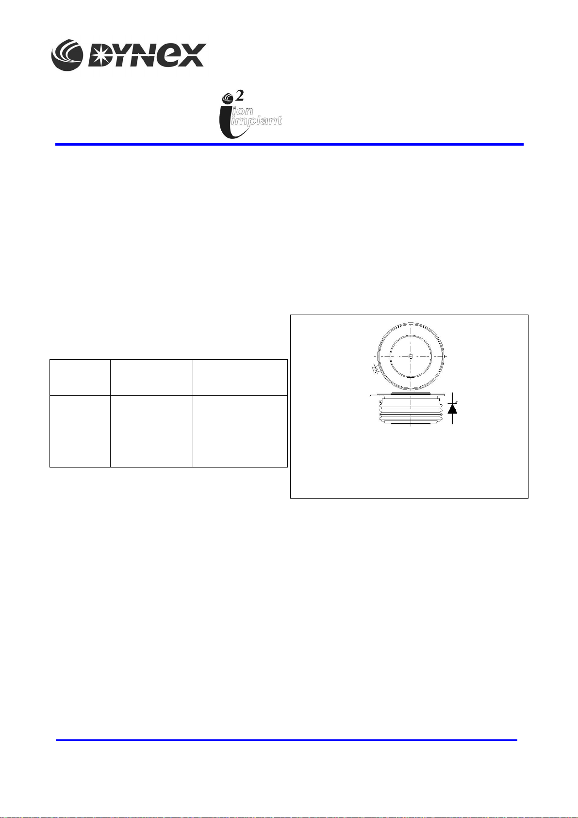
Outline type code: J
(See Package Details for further information)
Fig. 1 Package outline
DCR390J85
Phase Control Thyristor
Preliminary Informat ion
SEMICONDUCTOR
DCR390J85
2/9
www.dynexsemi.com
CURRENT RATINGS
T
case
= 60° C unless stated otherwise
Symbol
Parameter
Test Conditions Max. Units
Double Side Cooled
I
T(AV)
Mean on-state current Half wave resistive load 387 A
I
T(RMS)
RMS value - 608 A
I
T
Continuous (direct) on-state current - 583 A
SURGE RATINGS
Symbol
Parameter
Test Conditions Max. Units
I
TSM
Surge (non-repetitive) on-state current 10ms half sine, T
case
= 125°C 5.25 kA
I2t I2t for fusing VR = 0 0.138 MA2s
THERMAL AND MECHANICAL RATINGS
Symbol
Parameter
Test Conditions Min. Max. Units
R
th(j-c)
Thermal resistance – junction to case Double side cooled DC - 0.0379 ° C/W
Single side cooled Anode DC - 0.0745 ° C/W
Cathode DC - 0.0797 ° C/W
R
th(c-h)
Thermal resistance – case to heatsink Clamping force 11.5kN Double side - 0.0072 °C/W
(with mounting compound) Single side - .0144 °C/W
T
vj
Virtual junction temperature On-state (conducting) - 135 °C
Reverse (blocking) - 125 °C
T
stg
Storage temperature range -55 125 ° C
F
m
Clamping force 10 13 kN
SEMICONDUCTOR
DCR390J85
3/9
www.dynexsemi.com
DYNAMIC CHARACTERISTICS
Symbol
Parameter
Test Conditions Min. Max. Units
I
RRM/IDRM
Peak reverse and off-state current At V
RRM/VDRM
, T
case
= 125°C - 100 mA
dV/dt Max. linear rate of rise of off-state voltage To 67% V
DRM
, Tj = 125°C, gate open - 1500 V/µs
dI/dt Rate of rise of on-state current From 67% V
DRM
to 2x I
T(AV)
Repetitive 50Hz
- 100 A/µs
Gate source 30V, 10Ω,
Non-repetitive
- 200 A/µs
tr < 0.5µs, Tj = 125°C
V
T(TO)
Threshold voltage – Low l evel 50A to 400A at T
case
= 125°C - 1.162 V
Threshold voltage – High level 400A to 1600A at T
case
= 125°C - 1.3063 V
r
T
On-state slope resistance – Low level 50A to 400A at T
case
= 125°C - 3.153
mΩ
On-state slope resistance – High level 400A to 1600A at T
case
= 125°C - 2.763
mΩ
t
gd
Delay time
VD = 67% V
DRM
, gate source 30V, 10Ω
TBD TBD µs
tr = 0.5µs, Tj = 25°C
t
q
Turn-off time Tj = 125°C, VR = 200V, dI/dt = 5A/µs, 1000 1600 µs
dVDR/dt = 20V/µs linear
Q
S
Stored charge IT = 500A, Tj = 125°C, dI/dt = 5A/µs, 2000 2600 µC
I
L
Latching current Tj = 25°C, VD = 5V TBD TBD mA
I
H
Holding current
Tj = 25°C, R
G-K
= ∞, ITM = 500A, IT = 5A
TBD TBD mA

SEMICONDUCTOR
DCR390J85
4/9
www.dynexsemi.com
GATE TRIGGER CHARACTERISTICS AND RATINGS
Symbol
Parameter
Test Conditions Max. Units
V
GT
Gate trigger voltage V
DRM
= 5V, T
case
= 25°C 1.5 V
V
GD
Gate non-trigger voltage At V
DRM, Tcase
= 125°C TBD V
I
GT
Gate trigger current V
DRM
= 5V, T
case
= 25°C 250 mA
I
GD
Gate non-trigger current V
DRM
= 5V, T
case
= 25°C TBD mA
CURVES
0
400
800
1200
1600
1.0
2.0
3.0
4.0
5.0
Instantaneous on-state voltage V
T
- (V)
Instantaneous on-state current I
T
- (A)
25°C min
25°C max
125°C min
125°C max
Fig.2 Maximum & minimum on-state characteristics
VTM EQUATION
Where A = 1.545561
B = -0.202735
VTM = A + Bln (IT) + C.IT+D.√I
T
C = 0.001865
D = 0.066158
these values are valid for Tj = 125°C for IT 50A to 1600A

SEMICONDUCTOR
DCR390J85
5/9
www.dynexsemi.com
0
1
2
3
4
5
6
7
8
9
10
11
12
13
14
15
16
0
500
1000
1500
Mean on-state current, I
T(AV)
- (A)
Mean power dissipation - (kW)
180
120
90
60
30
0
10
20
30
40
50
60
70
80
90
100
110
120
130
0
100
200
300
400
500
600
Mean on-state current, I
T(AV)
- (A)
Maximum case temperature, T
case
(
o
C )
180
120
90
60
30
Fig.3 On-state power dissipation – sine wav e Fig.4 Maximum permissible case temperature,
double side cooled – sine wave
0
10
20
30
40
50
60
70
80
90
100
110
120
130
0
100
200
300
400
500
600
Mean on-state current, I
T(AV)
- (A )
Maximum heatsink temperature, T
Heatsink
- (
o
C )
180
120
90
60
30
0
1
2
3
4
5
6
7
8
9
10
11
12
0
500
1000
1500
2000
Mean on-state current, I
T(AV)
- (A)
Mean power dissipation - (kW)
d.c.
180
120
90
60
30
Fig.5 Maximum permissible heatsink temperature,
double side cooled – sine wave
Fig.6 On-state power dissipation – rectangular wave

SEMICONDUCTOR
DCR390J85
6/9
www.dynexsemi.com
0
10
20
30
40
50
60
70
80
90
100
110
120
130
0
100
200
300
400
500
600
700
800
900
Mean on-state current, I
T(AV)
- (A)
Maximum permissible case temperature , T
case
-
(°C)
d.c.
180
120
90
60
30
0
10
20
30
40
50
60
70
80
90
100
110
120
130
0
100
200
300
400
500
600
700
800
Mean on-state current, I
T(AV
) - (A)
Maximum heatsik temperature T
heatsink
- (
o
C)
d.c.
180
120
90
60
30
Fig.7 Maximum permissible case temperature,
double side cooled – rectangular wave
Fig.8 Maximum permissible heatsink temperature,
double side cooled – rectangular wave
0
10
20
30
40
50
60
70
80
90
0.001
0.01
0.1110
100
Time ( s )
Thermal impedance -Z
th
( °C/kW )
Double Side Cooled
Anode Cooled
Cathode Cooled
123
4
Double side cooled
Ri (° C/kW)
2.4256
9.3503
10.6963
15.3758
Ti (s)
0.0087759
0.053099
0.4497246
1.395
Anode side cooled
Ri (° C/kW)
2.8091
9.5576
11.3564
50.6136
Ti (s)
0.0097443
0.0591913
0.4759179
6.5548
Cathode side cooled
Ri (° C/kW)
2.9507
9.4031
11.0771
56.0405
Ti (s)
0.0100391
0.0606056
0.4732916
7.228
Zth = Σ [Ri x ( 1-exp. (t/t
i
))]
[1]
∆
R
th(j-c)
Conduction
Tables show the increments of thermal resistance R
th(j-c)
when the device
operates at conduction angles other than d.c.
Double side cooling
Anode Side Cooling
Cathode Sided Cooling
∆
Zth (z)∆Zth (z)∆Zth (z)
°
sine.
rect.°sine.
rect.°sine.
rect.
180
4.43
3.01
180
4.39
2.99
180
4.37
2.98
120
5.13
4.30
120
5.07
4.26
120
5.05
4.25
90
5.89
5.03905.81
4.97905.79
4.96
60
6.58
5.81606.48
5.74606.45
5.72
30
7.12
6.67307.00
6.57306.97
6.54
15
7.36
7.13157.24
7.01157.20
6.98
Fig.9 Maximum (limit) transient thermal impedance – junction to case (°C/kW)
SEMICONDUCTOR
DCR390J85
7/9
www.dynexsemi.com
0
1
2
3
4
5
6
110100
Number of cycles
Surge current, I
TSM
- (kA)
Conditions:
Tcase = 125° C
VR =0
Pulse width = 10ms
0
1
2
3
4
5
6
7
8
9
10
11
12
13
110100
Pulse width, t
P
- (ms)
Surge current, I
TSM
- (kA)
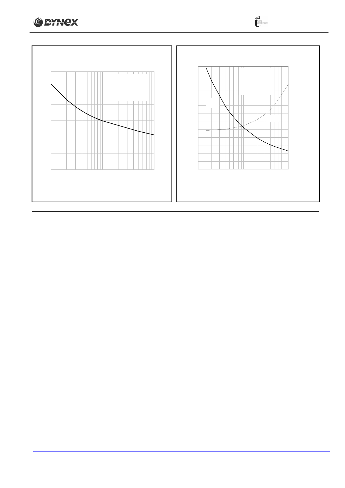
0
0.05
0.1
0.15
0.2
0.25
0.3
I
2
t (MA
2
s)
I2t
I
TSM
Conditions:
T
case
= 125° C
VR = 0
half-sine wave
Fig.10 Multi-cycle surge current Fig.11 Single-cycle surge current

SEMICONDUCTOR
DCR390J85
8/9
www.dynexsemi.com
PACKAGE DETAILS
For further package information, please contact Customer Services. All dimensions in mm, unless stated otherwise.
DO NOT SCALE.
3rd ANGLE PROJECTION
IF IN DOUBT ASK
DO NOT SCALE
CATHODE
20° OFFSET (NOM.)
TO GATE TUBE
FOR PACKAGE
HEIGHT SEE TABLE
Ø1.5
ANODE
GATE
Ø33.95 NOM
Ø57.0 MAX
Ø33.95 NOM
ELECTRODES)
DEEP (IN BOTH
HOLE Ø3.60 X 2.00
Device
Maximum
Thickness
(mm)
Minimum
Thickness
(mm)
DCR880J22
34.465
33.915
DCR780J28
34.54
33.99
DCR640J42
34.77
34.22
DCR570J52
34.89
34.34
DCR490J65
35.15
34.6
DCR390J85
35.51
34.96
Clamping force: 11.5 kN ±10%
Lead length: 420mm
Lead terminal connector: M4 ring
Package outline type code: J
Fig.15 Package outline

SEMICONDUCTOR
DCR390J85
9/9
www.dynexsemi.com
POWER ASSEMBLY CAPABILITY
The Power Assembly group was set up to provide a support service for those customers requiring more than the basic
semiconductor, and has developed a flexible range of heatsink and clamping systems in line with advances in device voltages
and current capability of our semiconductors.
We offer an extensive range of air and liquid cooled assemblies covering the full range of circuit designs in general use today.
The Assembly group offers high quality engineering support dedicated to designing new units to satisfy the growing needs of our
customers.
Using the latest CAD methods our team of design and applications engineers aim to provide the Power Assembly Complete
Solution (PACs).
HEATSINKS
The Power Assembly group has its own proprietary range of extruded aluminium heatsinks which have been designed to optimise
the performance of Dynex semiconductors. Data with respect to air natural, forced air and liquid cooling (with flow rates) is
available on request.
For further information on device clamps, heatsinks and assemblies, please contact your nearest sales representative or
Customer Services.
Stresses above those listed in this data sheet may cause permanent damage to the device. In extreme conditions, as with all
semiconductors, this may include potentially hazardous rupture of the package. Appropriate safety precautions should always be
followed.
http://www.dynexsemi.com
e-mail: power_solutions@dynexsemi.com
HEADQUARTERS OPERATIONS CUSTOMER SERVICE
DYNEX SEMICONDUCTOR LTD
Tel: +44(0)1522 502753 / 502901. Fax: +44(0)1522 500020
Doddington Road, Lincoln
Lincolnshire, LN6 3LF. United Kingdom.
Tel: +44(0)1522 500500
Fax: +44(0)1522 500550
Dynex Semiconductor 2003 TECHNICAL DOCUMENTATION – NOT FOR
RESALE. PRODUCED IN UNITED KINGDOM.
This publication is issued to provide information only which (unless agreed by the Company in writing) may not be used, applied or reproduced for any purpose nor form part of any order or
contract nor to be regarded as a representation relating to the products or services concerned. No warranty or guarantee express or implied is made regarding the capability, performance or
suitability of any product or service. The Company reserves the right to alter without prior notice the specification, design or price of any product or service. Information concerning possible
methods of use is provided as a guide only and does not constitute any guarantee that such methods of use will be satisfactory in a specific piece of equipment. It is the user’s responsibility to
fully determine the performance and suitability of any equipment using such information and to ensure that any publication or data used is up to date and has not been superseded. These
products are not suitable for use in any medical products whose failure to perform may result in significant injury or death to the user. All products and materials are sold and services provided
subject to the Company’s conditions of sale, which are available on request.
All brand names and product names used in this publication are trademarks, registered trademarks or trade names of their respective owners.
 Loading...