

Page 1
SERVICE MANUAL
Main Section
I Specifications
I Preparation for Servicing
I Adjustment Procedures
I Schematic Diagrams
I CBA’s
I Exploded Views
I Parts List
When servicing the deck
mechanism, refer to MK14 Deck
Mechanism Section.
Deck Mechanism Part No.:
N2326FT or N2526FT
14″ COLOR TV/VCR COMBINATION
T6609BK
PAL
Page 2

MAIN SECTION
14″ COLOR TV/VCR COMBINATION
T6609BK
Main Section
I Specifications
I Preparation for Servicing
I Adjustment Procedures
I Schematic Diagrams
I CBA’s
I Exploded Views
I Parts List
TABLE OF CONTENTS
Specifications . . . . . . . . . . . . . . . . . . . . . . . . . . . . . . . . . . . . . . . . . . . . . . . . . . . . . . . . . . . . . . . . . . . . . . . . . . 1-1-1
Important Safety Precautions. . . . . . . . . . . . . . . . . . . . . . . . . . . . . . . . . . . . . . . . . . . . . . . . . . . . . . . . . . . . . . 1-2-1
Standard Notes for Servicing . . . . . . . . . . . . . . . . . . . . . . . . . . . . . . . . . . . . . . . . . . . . . . . . . . . . . . . . . . . . . . 1-3-1
Preparation for Servicing . . . . . . . . . . . . . . . . . . . . . . . . . . . . . . . . . . . . . . . . . . . . . . . . . . . . . . . . . . . . . . . . . 1-4-1
Cabinet Disassembly Instructions . . . . . . . . . . . . . . . . . . . . . . . . . . . . . . . . . . . . . . . . . . . . . . . . . . . . . . . . . . 1-5-1
Electrical Adjustment Instructions . . . . . . . . . . . . . . . . . . . . . . . . . . . . . . . . . . . . . . . . . . . . . . . . . . . . . . . . . . 1-6-1
How to Initialize the TV/VCR Combination. . . . . . . . . . . . . . . . . . . . . . . . . . . . . . . . . . . . . . . . . . . . . . . . . . . . 1-7-1
Mechanical Trouble Indicator . . . . . . . . . . . . . . . . . . . . . . . . . . . . . . . . . . . . . . . . . . . . . . . . . . . . . . . . . . . . . . 1-8-1
Block Diagrams . . . . . . . . . . . . . . . . . . . . . . . . . . . . . . . . . . . . . . . . . . . . . . . . . . . . . . . . . . . . . . . . . . . . . . . . 1-9-1
Schematic Diagrams / CBA’s and Test Points . . . . . . . . . . . . . . . . . . . . . . . . . . . . . . . . . . . . . . . . . . . . . . . . 1-10-1
Waveforms . . . . . . . . . . . . . . . . . . . . . . . . . . . . . . . . . . . . . . . . . . . . . . . . . . . . . . . . . . . . . . . . . . . . . . . . . . . 1-11-1
Wiring Diagram . . . . . . . . . . . . . . . . . . . . . . . . . . . . . . . . . . . . . . . . . . . . . . . . . . . . . . . . . . . . . . . . . . . . . . . 1-12-1
System Control Timing Charts . . . . . . . . . . . . . . . . . . . . . . . . . . . . . . . . . . . . . . . . . . . . . . . . . . . . . . . . . . . . 1-13-1
IC Pin Function Descriptions . . . . . . . . . . . . . . . . . . . . . . . . . . . . . . . . . . . . . . . . . . . . . . . . . . . . . . . . . . . . . 1-14-1
Lead Identifications . . . . . . . . . . . . . . . . . . . . . . . . . . . . . . . . . . . . . . . . . . . . . . . . . . . . . . . . . . . . . . . . . . . . 1-15-1
Exploded Views . . . . . . . . . . . . . . . . . . . . . . . . . . . . . . . . . . . . . . . . . . . . . . . . . . . . . . . . . . . . . . . . . . . . . . . 1-16-1
Mechanical Parts List . . . . . . . . . . . . . . . . . . . . . . . . . . . . . . . . . . . . . . . . . . . . . . . . . . . . . . . . . . . . . . . . . . . 1-17-1
Electrical Parts List . . . . . . . . . . . . . . . . . . . . . . . . . . . . . . . . . . . . . . . . . . . . . . . . . . . . . . . . . . . . . . . . . . . . 1-18-1
Page 3
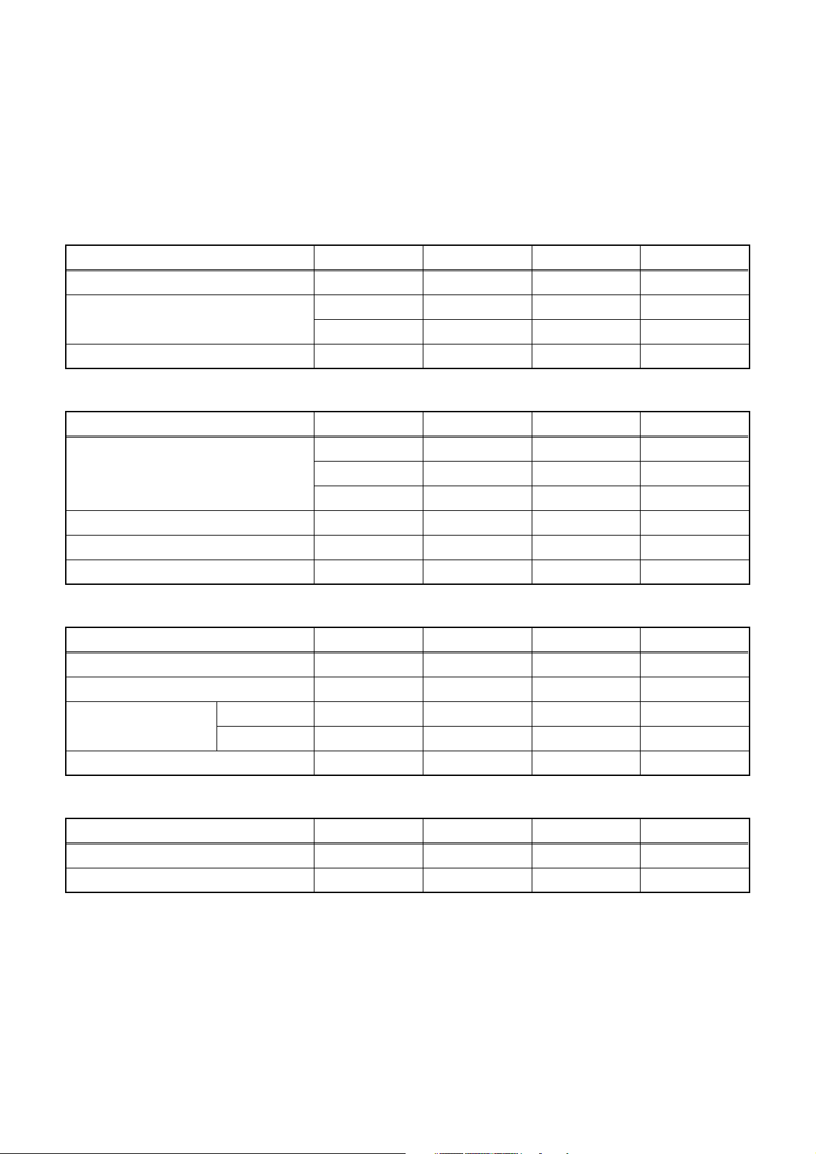
SPECIFICATIONS
*ˆ Mode---------SP mode unless otherwise specified
* Test input terminal
<Except Tuner>--------Video input (1 Vp-p)
Audio input (-10 dB)
<Tuner>------------------Ant. input (80 dBµV) Video: 87.5% mod.(BG/DK), 80.0% mod.(I)
Audio: 30 kHz dev. (1 kHz Sin)
< DEFLECTION >
Description Condition Unit Nominal Limit
1. Over Scan --- % 90 85/95
2. Linearity
3. High Voltage --- kV 22 ---
Horizontal % --- ±15
Vertical % --- ±10
< VIDEO & CHROMA >
Description Condition Unit Nominal Limit
Center m/m --- 0.6
1. Misconvergence
2. Contrast Control Range --- dB --- 6
3. Brightness APL 100% ft-L 55 40
4. Color Temperature --- K 8500 ---
Corner m/m --- 2.0
Side m/m --- 1.5
< VCR >
Description Condition Unit Nominal Limit
1. Horizontal Resolution (R/P) Line 230 200
2. Jitter (Low) (R/P) µs 0.05 0.2
3. S/N Chroma
4. Wow & Flutter (RMS) (R/P) % 0.25 0.5
AM(SP) (R/P) dB 38 33
PM(SP) (R/P) dB 36 33
< TUNER >
Description Condition Unit Nominal Limit
1. Video S/N --- dB 45 40
2. Audio S/N (W/LPF) --- dB 43 40
1-1-1 T6609SP
Page 4
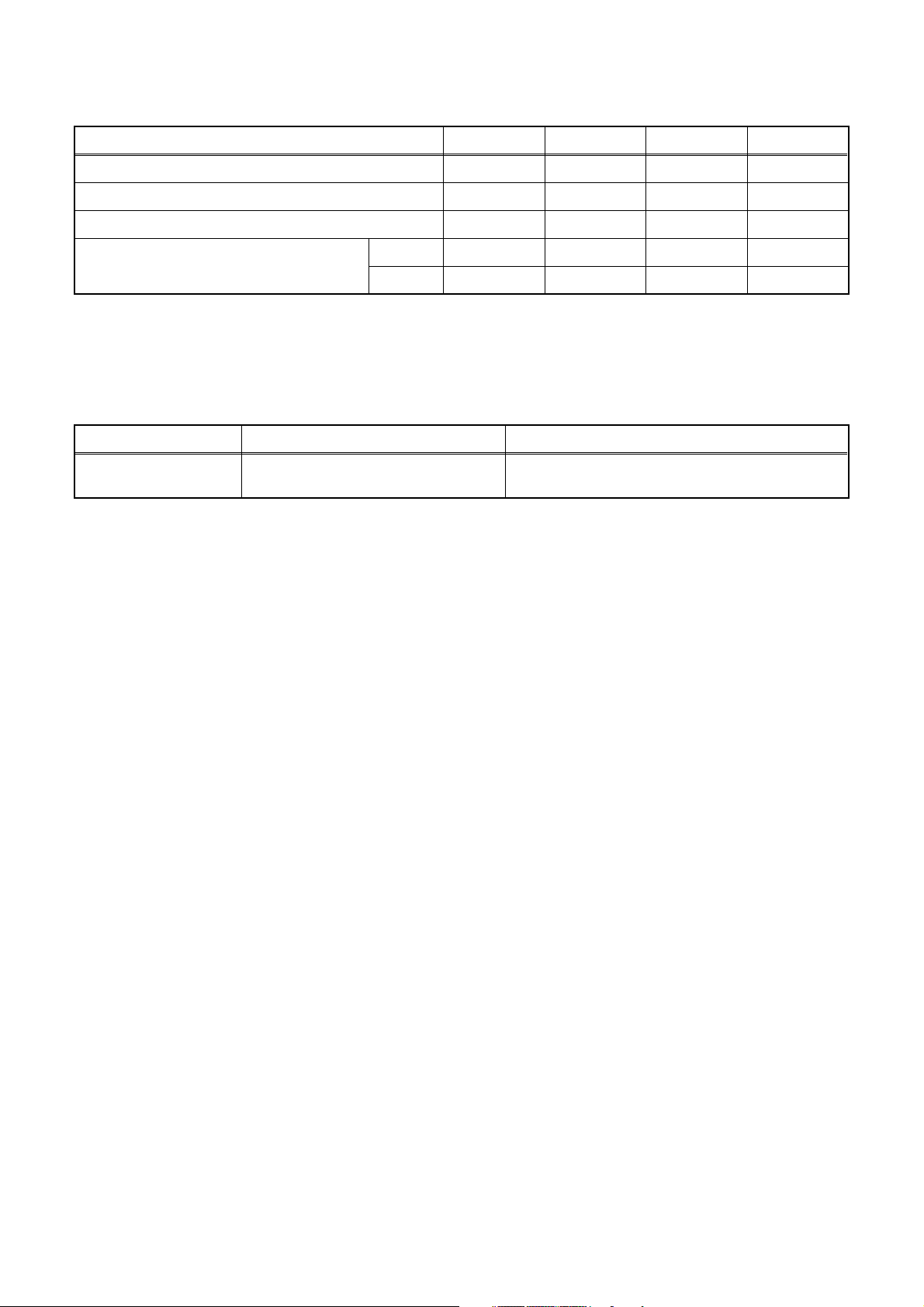
< AUDIO>
All items are measured across 8 Ω resistor at speaker output terminal.
Description Condition Unit Nominal Limit
1. Audio Output Power (Max.) (R/P) W 1.0 0.8
2. Audio S/N (W/LPF) (R/P) dB 40 36
3. Audio distortion (W/LPF) (R/P) % 3.0 5.0
4. Audio Freq. Response
(-20dB Ref. 1kHz)
Note: Nominal specifications represent the design specifications. All units should be able to approximate these.
Some will exceed and some may drop slightly below these specifications. Limit specifications represent
the absolute worst condition that still might be considered acceptable. In no case should a unit fail to meet
limit specifications.
200 Hz (R/P) dB --- 5.0/-10
6 kHz (R/P) dB --- 5.0/-10
<TV NORM, TUNER SENSIVITY, RECEPTIVE TV CHANNELS>
TV Norm Tuner Sensivity Receptive TV Channels
PA L -I
NOM: VHF 46dBµV / UHF 47dBµV
MAX: VHF 53dBµV / UHF 56dBµV
IRA - IRJ, gapC, E21 - E69, S01 - S03,
Z+1, Z+2, S1 - S41
1-1-2 T6609SP
Page 5
IMPORTANT SAFETY PRECAUTIONS
Prior to shipment from the factory, our products are strictly inspected for recognized product safety and electrical
codes of the countries in which they are to be sold. However, in order to maintain such compliance, it is equally
important to implement the following precautions when a set is being serviced.
Safety Precautions for TV Circuit
1. Before returning an instrument to the
customer, always make a safety check of the
entire instrument, including, but not limited to, the
following items:
a. Be sure that no built-in protective devices are
defective and have been defeated during
servicing. (1) Protective shields are provided
on this chassis to protect both the technician
and the customer. Correctly replace all missing
protective shields, including any removed for
servicing convenience. (2) When reinstalling
the chassis and/or other assembly in the
cabinet, be sure to put back in place all
protective devices, including but not limited to,
nonmetallic control knobs, insulating
fishpapers, adjustment and compartment
covers/shields, and isolation resistor/capacitor
networks. Do not operate this instrument or
permit it to be operated without all
protective devices correctly installed and
functioning. Servicers who defeat safety
features or fail to perform safety checks
may be liable for any resulting damage.
b. Be sure that there are no cabinet openings
through which an adult or child might be able to
insert their fingers and contact a hazardous
voltage. Such openings include, but are not
limited to, (1) spacing between the picture tube
and the cabinet mask, (2) excessively wide
cabinet ventilation slots, and (3) an improperly
fitted and/or incorrectly secured cabinet back
cover.
c. Antenna Cold Check - With the instrument AC
plug removed from any AC source, connect an
electrical jumper across the two AC plug
prongs. Place the instrument AC switch in the
on position. Connect one lead of an ohmmeter
to the AC plug prongs tied together and touch
the other ohmmeter lead in turn to each tuner
antenna input exposed terminal screw and, if
applicable, to the coaxial connector. If the
measured resistance is less than 1.0 megohm
or greater than 5.2 megohm, an abnormality
exists that must be corrected before the
instrument is returned to the customer. Repeat
this test with the instrument AC switch in the off
position.
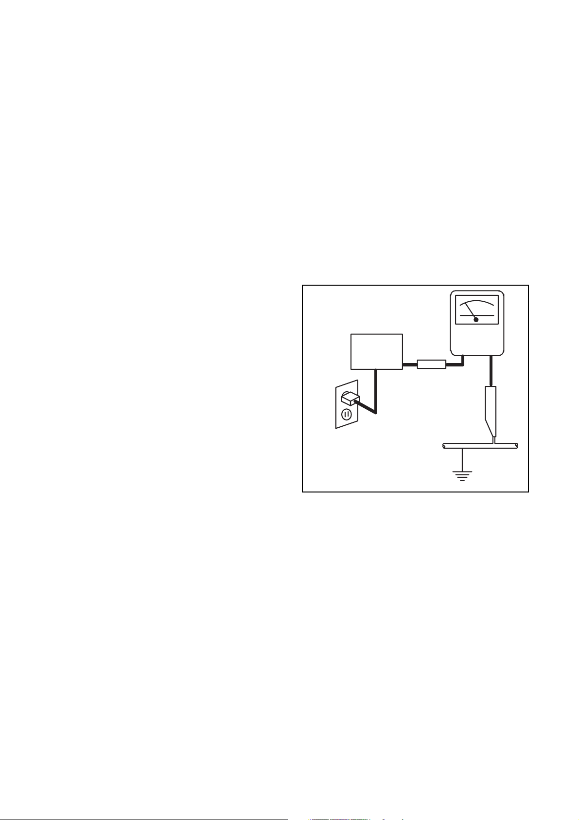
d. Leakage Current Hot Check - With the
instrument completely reassembled, plug the
AC line cord directly into a 120 V AC outlet. (Do
not use an isolation transformer during this
test.) Use a leakage current tester or a
metering system that complies with American
National Standards Institute (ANSI) C101.1
Leakage Current for Appliances and
Underwriters Laboratories (UL) 1410, (50.7).
With the instrument AC switch first in the on
position and then in the off position, measure
from a known earth ground (metal water pipe,
conduit, etc.) to all exposed metal parts of the
instrument (antennas, handle brackets, metal
cabinet, screw heads, metallic overlays, control
shafts, etc.), especially any exposed metal
parts that offer an electrical return path to the
chassis. Any current measured must not
exceed 0.5 milli-ampere. Reverse the
instrument power cord plug in the outlet and
repeat the test.
READING SHOULD
NOT BE ABOVE 0.5 mA
LEAKAGE
DEVICE
BEING
TESTED
TEST ALL EXPOSED
METAL SURFACES
ALSO TEST WITH
PLUG REVERSED
USING AC
ADAPTER PLUG
AS REQUIRED
ANY MEASUREMENTS NOT WITHIN THE
LIMITS SPECIFIED HEREIN INDICATE A
POTENTIAL SHOCK HAZARD THAT MUST
BE ELIMINATED BEFORE RETURNING THE
INSTRUMENT TO THE CUSTOMER OR
BEFORE CONNECTING THE ANTENNA OR
ACCESSORIES.
e. X-Radiation and High Voltage Limits -
Because the picture tube is the primary
potential source of X-radiation in solid-state TV
receivers, it is specially constructed to prohibit
X-radiation emissions. For continued
X-radiation protection, the replacement picture
tube must be the same type as the original.
Also, because the picture tube shields and
mounting hardware perform an X-radiation
protection function, they must be correctly in
place. High voltage must be measured each
time servicing is performed that involves B+,
horizontal deflection or high voltage. Correct
operation of the X-radiation protection circuits
also must be reconfirmed each time they are
serviced. (X-radiation protection circuits also
CURRENT
TESTER
+
EARTH
GROUND
_
1-2-1 TVVCRP_ISP
Page 6

may be called “horizontal disable” or “hold
down.”) Read and apply the high voltage limits
and, if the chassis is so equipped, the
X-radiation protection circuit specifications
given on instrument labels and in the Product
Safety & X-Radiation Warning note on the
service data chassis schematic. High voltage is
maintained within specified limits by close
tolerance safety-related components/
adjustments in the high-voltage circuit. If high
voltage exceeds specified limits, check each
component specified on the chassis schematic
and take corrective action.
2. Read and comply with all caution and
safety-related notes on or inside the receiver
cabinet, on the receiver chassis, or on the picture
tube.
3. Design Alteration Warning - Do not alter or add
to the mechanical or electrical design of this TV
receiver. Design alterations and additions,
including, but not limited to circuit modifications
and the addition of items such as auxiliary audio
and/or video output connections, might alter the
safety characteristics of this receiver and create a
hazard to the user. Any design alterations or
additions will void the manufacturer's warranty and
may make you, the servicer, responsible for
personal injury or property damage resulting
therefrom.
4. Picture Tube Implosion Protection Warning -
The picture tube in this receiver employs integral
implosion protection. For continued implosion
protection, replace the picture tube only with one
of the same type number. Do not remove, install,
or otherwise handle the picture tube in any
manner without first putting on shatterproof
goggles equipped with side shields. People not so
equipped must be kept safely away while picture
tubes are handled. Keep the picture tube away
from your body. Do not handle the picture tube by
its neck. Some “in-line” picture tubes are equipped
with a permanently attached deflection yoke;
because of potential hazard, do not try to remove
such “permanently attached” yokes from the
picture tube.
5. Hot Chassis Warning -
a. Some TV receiver chassis are electrically
connected directly to one conductor of the AC
power cord and maybe safety-serviced without
an isolation transformer only if the AC power
plug is inserted so that the chassis is
connected to the ground side of the AC power
source. To confirm that the AC power plug is
inserted correctly, with an AC voltmeter,
measure between the chassis and a known
earth ground. If a voltage reading in excess of
1.0V is obtained, remove and reinsert the AC
power plug in the opposite polarity and again
measure the voltage potential between the
chassis and a known earth ground.
b. Some TV receiver chassis normally have 85V
AC(RMS) between chassis and earth ground
regardless of the AC plug polarity. This chassis
can be safety-serviced only with an isolation
transformer inserted in the power line between
the receiver and the AC power source, for both
personnel and test equipment protection.
c. Some TV receiver chassis have a secondary
ground system in addition to the main chassis
ground. This secondary ground system is not
isolated from the AC power line. The two
ground systems are electrically separated by
insulation material that must not be defeated or
altered.
6. Observe original lead dress. Take extra care to
assure correct lead dress in the following areas: a.
near sharp edges, b. near thermally hot parts-be
sure that leads and components do not touch
thermally hot parts, c. the AC supply, d. high
voltage, and e. antenna wiring. Always inspect in
all areas for pinched, out of place, or frayed wiring.
Check AC power cord for damage.
7. Components, parts, and/or wiring that appear to
have overheated or are otherwise damaged
should be replaced with components, parts, or
wiring that meet original specifications.
Additionally, determine the cause of overheating
and/or damage and, if necessary, take corrective
action to remove any potential safety hazard.
8. Product Safety Notice - Some electrical and
mechanical parts have special safety-related
characteristics which are often not evident from
visual inspection, nor can the protection they give
necessarily be obtained by replacing them with
components rated for higher voltage, wattage, etc.
Parts that have special safety characteristics are
identified by a ! on schematics and in parts lists.
Use of a substitute replacement that does not
have the same safety characteristics as the
recommended replacement part might create
shock, fire, and/or other hazards. The Product's
Safety is under review continuously and new
instructions are issued whenever appropriate.
Prior to shipment from the factory, our products
are strictly inspected to confirm with the
recognized product safety and electrical codes of
the countries in which they are to be sold.
However, in order to maintain such compliance, it
is equally important to implement the following
precautions when a set is being serviced.
Precautions during Servicing
A. Parts identified by the ! symbol are critical for
safety.
Replace only with part number specified.
B. In addition to safety, other parts and assemblies
are specified for conformance with regulations
applying to spurious radiation. These must also be
replaced only with specified replacements.
Examples: RF converters, RF cables, noise
blocking capacitors, and noise blocking filters, etc.
1-2-2 TVVCRP_ISP
Page 7

C. Use specified internal wiring. Note especially:
1) Wires covered with PVC tubing
2) Double insulated wires
3) High voltage leads
D. Use specified insulating materials for hazardous
live parts. Note especially:
1) Insulation Tape
2) PVC tubing
3) Spacers
4) Insulators for transistors.
E. When replacing AC primary side components
(transformers, power cord, etc.), wrap ends of
wires securely about the terminals before
soldering.
F. Observe that the wires do not contact heat
producing parts (heat sinks, oxide metal film
resistors, fusible resistors, etc.)
G. Check that replaced wires do not contact sharp
edged or pointed parts.
H. When a power cord has been replaced, check that
5~6 kg of force in any direction will not loosen it.
I. Also check areas surrounding repaired locations.
J. Use care that foreign objects (screws, solder
droplets, etc.) do not remain inside the set.
K. Crimp type wire connector
When replacing the power transformer in sets
where the connections between the power cord
and power transformer primary lead wires are
performed using crimp type connectors, in order to
prevent shock hazards, perform carefully and
precisely the following steps.
Replacement procedure
1) Remove the old connector by cutting the wires
at a point close to the connector.
Important: Do not re-use a connector (discard
it).
2) Strip about 15 mm of the insulation from the
ends of the wires. If the wires are stranded,
twist the strands to avoid frayed conductors.
3) Align the lengths of the wires to be connected.
Insert the wires fully into the connector.
4) Use the crimping tool to crimp the metal sleeve
at the center position. Be sure to crimp fully to
the complete closure of the tool.
L. When connecting or disconnecting the VCR
connectors, first, disconnect the AC plug from AC
supply socket.
1-2-3 TVVCRP_ISP
Page 8
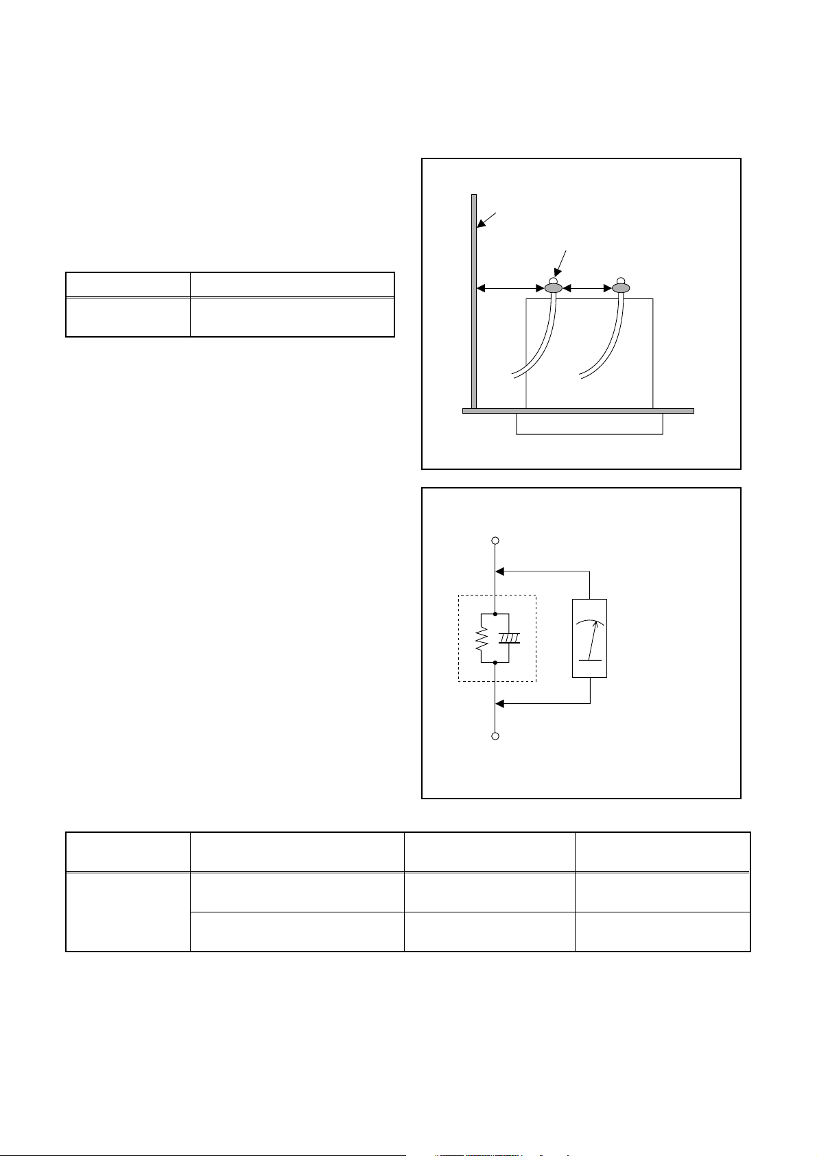
Safety Check after Servicing
Examine the area surrounding the repaired location for damage or deterioration. Observe that screws, parts and
wires have been returned to original positions. Afterwards, perform the following tests and confirm the specified
values in order to verify compliance with safety standards.
1. Clearance Distance
When replacing primary circuit components, confirm
specified clearance distance (d) and (d') between
soldered terminals, and between terminals and
surrounding metallic parts. (See Fig. 1)
Table 1: Ratings for selected area
Chassis or Secondary Conductor
Primary Circuit Terminals
AC Line Voltage Clearance Distance (d), (d’)
220 to 240 V
Note: This table is unofficial and for reference only. Be
sure to confirm the precise values.
≥ 3 mm (d)
≥ 6 mm (d’)
2. Leakage Current Test
Confirm the specified (or lower) leakage current
between B (earth ground, power cord plug prongs) and
externally exposed accessible parts (RF terminals,
antenna terminals, video and audio input and output
terminals, microphone jacks, earphone jacks, etc.).
Measuring Method: (Power ON)
Insert load Z between B (earth ground, power cord plug
prongs) and exposed accessible parts. Use an AC
voltmeter to measure across both terminals of load Z.
See Fig. 2 and following table.
dd'
Fig. 1
Exposed Accessible Part
Z
AC Voltmeter
(High Impedance)
Earth Ground
B
Power Cord Plug Prongs
Table 2: Leakage current ratings for selected areas
AC Line Voltage Load Z Leakage Current (i)
2 kΩ RES. Connected in parallel
220 to 240 V
50 kΩ RES. Connected in parallel
Note: This table is unofficial and for reference only. Be sure to confirm the precise values.
i ≤ 0.7 mA AC Peak
i ≤ 2 mA DC
i ≤ 0.7 mA AC Peak
i ≤ 2 mA DC
1-2-4 TVVCRP_ISP
One side of power cord
plug prongs (B) to:
RF or Antenna terminals
Fig. 2
A/V Input, Output
Page 9
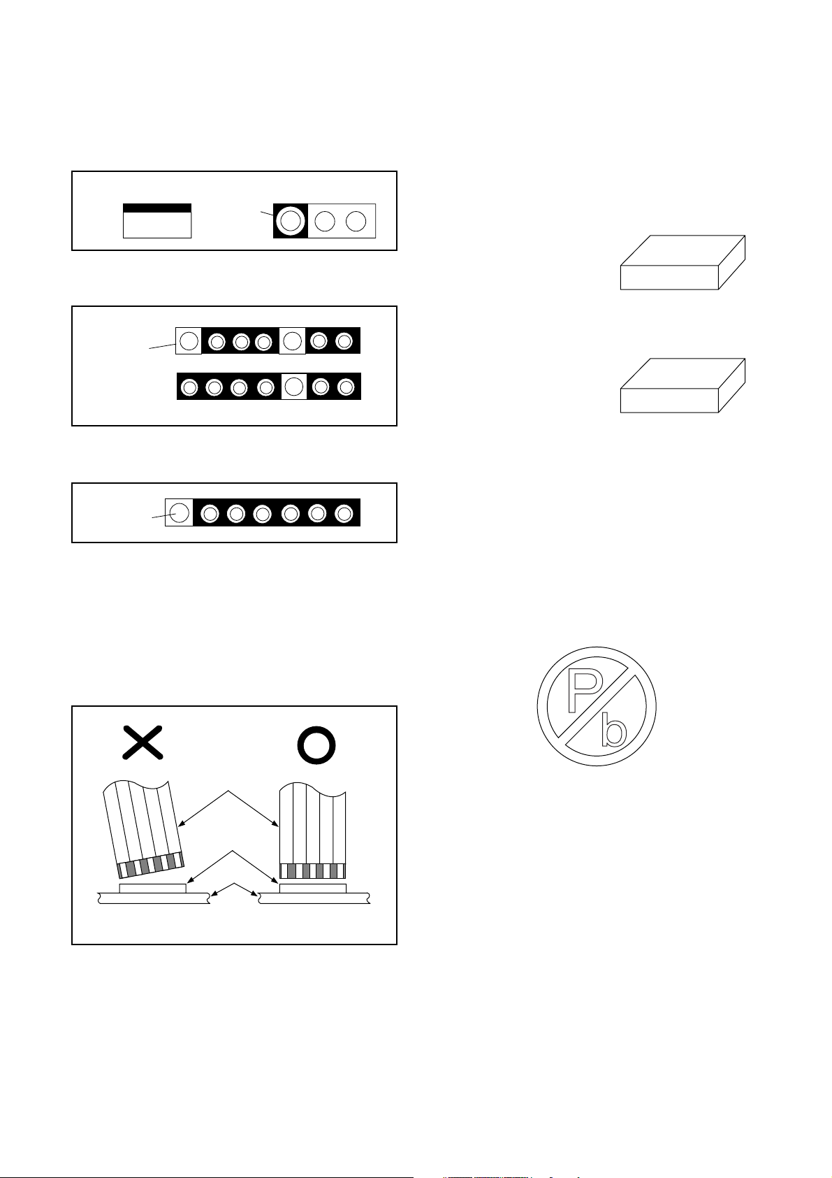
STANDARD NOTES FOR SERVICING
Circuit Board Indications
1. The output pin of the 3 pin Regulator ICs is
indicated as shown.
Top View
Out
2. For other ICs, pin 1 and every fifth pin are
indicated as shown.
Pin 1
3. The 1st pin of every male connector is indicated as
shown.
Pin 1
Input
In
Bottom View
5
10
How to Read the Values of the
Rectangular Type Chip
Components
Example:
(a) Resistor
473
= 473 = 47 [kΩ]
(b) Capacitor
= Not shown
Caution:
Once chip parts (Resistors, Capacitors, Transistors,
etc.) are removed, they must not be reused. Always
use a new part.
(Top View)
(Top View)
Instructions for Connectors
1. When you connect or disconnect the FFC (Flexible
Foil Connector) cable, be sure to first disconnect
the AC cord.
2. FFC (Flexible Foil Connector) cable should be
inserted parallel into the connector, not at an
angle.
FFC Cable
Connector
CBA
* Be careful to avoid a short circuit.
Pb (Lead) Free Solder
Pb free mark will be found on PCBs which use Pb
free solder. (Refer to figure.) For PCBs with Pb free
mark, be sure to use Pb free solder. For PCBs
without Pb free mark, use standard solder.
Pb free mark
1-3-1 TVVCRP_SN
Page 10
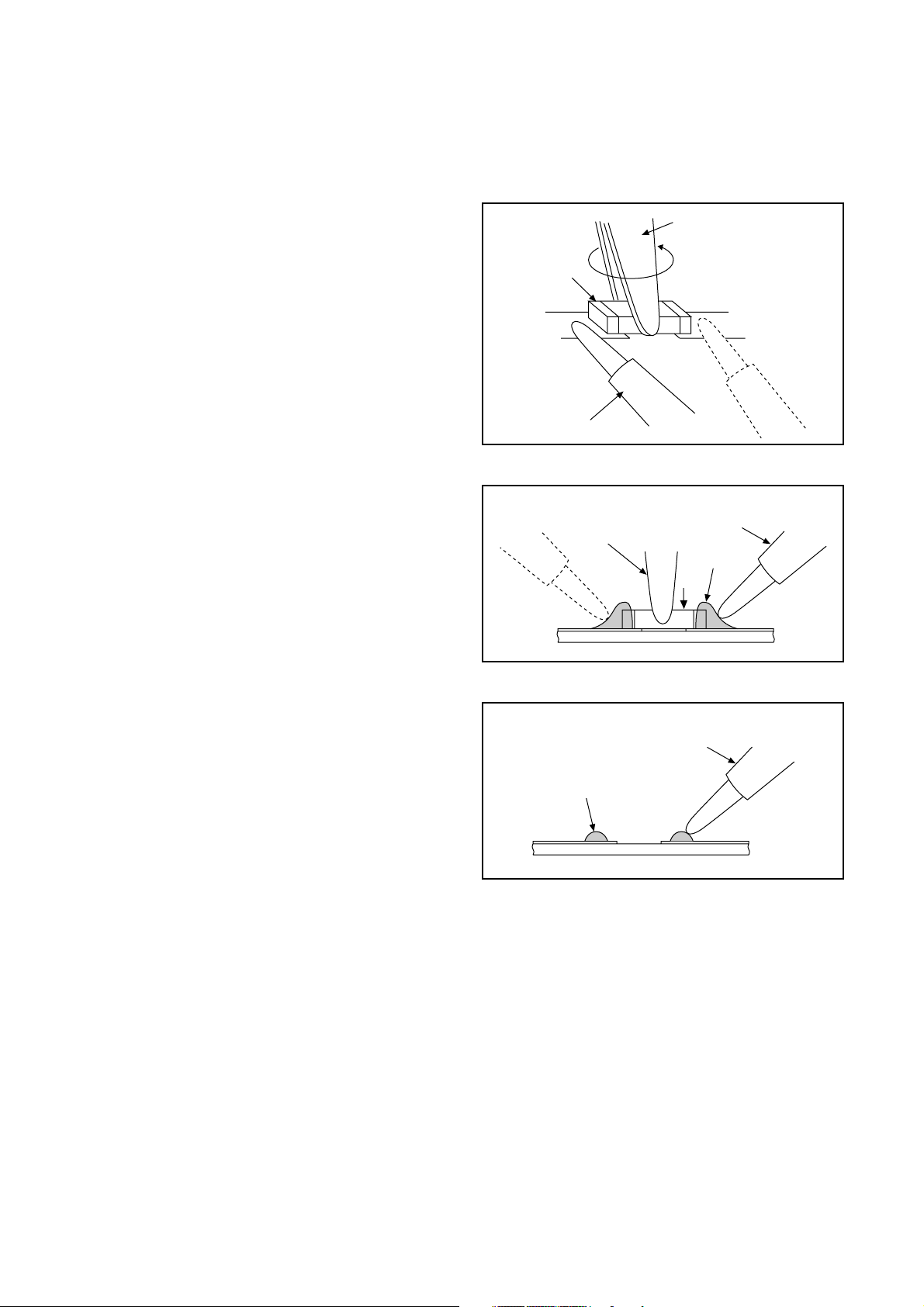
Replacement Procedures for
Leadless (Chip) Components
The Following Procedures are
Recommended for the Replacement of the
Leadless Components Used in this Unit.
3. Installing the leadless component
a. Presolder the contact points of the circuit board.
b. Press the part downward with tweezers and solder
both electrodes as shown below.
Note: Do not glue the replacement leadless
component to the circuit board.
1. Preparation for replacement
1-1. Pb free solder
a. Soldering Iron
Use a soldering iron for Pb free solder.
b. Solder
Be sure to use Pb free solder.
c. Soldering time
Do not apply heat for more than 4 seconds.
d. Preheating
Leadless capacitor must be preheated before
installation. (130 °C ~ 150 °C, for about two
minutes.)
1-2. Standard solder
a. Soldering Iron
Use a pencil-type soldering iron (less than 30
watts).
b. Solder
Eutectic solder (Tin 63%, Lead 37%) is
recommended.
c. Soldering time
Do not apply heat for more than 4 seconds.
d. Preheating
Leadless capacitor must be preheated before
installation. (130 °C ~ 150 °C, for about two
minutes.)
Chip
Soldering Iron
Tweezers
Tweezers
Soldering Iron
Solder
Note:
a. Leadless components must not be reused after
removal.
b. Excessive mechanical stress and rubbing for
the component electrode must be avoided.
2. Removing the leadless component
Grasp the leadless component body with tweezers
and alternately apply heat to both electrodes. When
the solder on both electrodes has melted, remove
leadless component with a twisting motion.
Note:
a. Do not attempt to lift the component off the
board until the component is completely
disconnected from the board by the twisting
action.
b. Take care not to break the copper foil on the
printed board
Soldering Iron
Presolder
1-3-2 TVVCRP_SN
Page 11
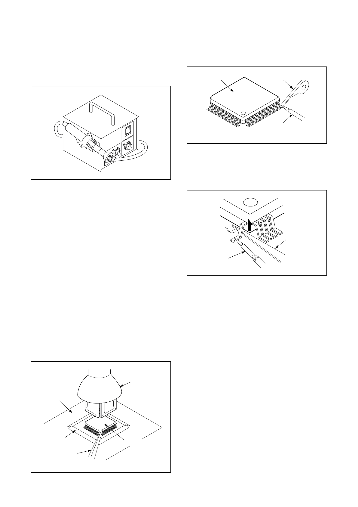
How to Remove / Install Flat Pack-IC
1. Removal
With Hot-Air Flat Pack-IC Desoldering Machine:
1. Prepare the hot-air flat pack-IC desoldering
machine, then apply hot air to the Flat Pack-IC
(about 5 to 6 seconds). (Fig. S-1-1)
Fig. S-1-1
2. Remove the flat pack-IC with tweezers while
applying the hot air.
3. Bottom of the flat pack-IC is fixed with glue to the
CBA; when removing entire flat pack-IC, first apply
soldering iron to center of the flat pack-IC and heat
up. Then remove (glue will be melted). (Fig. S-1-6)
4. Release the flat pack-IC from the CBA using
tweezers. (Fig. S-1-6)
CAUTION:
1. The Flat Pack-IC shape may differ by models. Use
an appropriate hot-air flat pack-IC desoldering
machine, whose shape matches that of the Flat
Pack-IC.
2. Do not supply hot air to the chip parts around the
flat pack-IC for over 6 seconds because damage
to the chip parts may occur. Put masking tape
around the flat pack-IC to protect other parts from
damage. (Fig. S-1-2)
3. The flat pack-IC on the CBA is affixed with glue, so
be careful not to break or damage the foil of each
pin or the solder lands under the IC when
removing it.
Hot-air
Flat Pack-IC
Desoldering
CBA
Masking
Tape
Tweezers
Machine
Flat Pack-IC
Fig. S-1-2
With Soldering Iron:
1. Using desoldering braid, remove the solder from
all pins of the flat pack-IC. When you use solder
flux which is applied to all pins of the flat pack-IC,
you can remove it easily. (Fig. S-1-3)
Flat Pack-IC
2. Lift each lead of the flat pack-IC upward one by
one, using a sharp pin or wire to which solder will
not adhere (iron wire). When heating the pins, use
a fine tip soldering iron or a hot air desoldering
machine. (Fig. S-1-4)
Fine Tip
Soldering Iron
3. Bottom of the flat pack-IC is fixed with glue to the
CBA; when removing entire flat pack-IC, first apply
soldering iron to center of the flat pack-IC and heat
up. Then remove (glue will be melted). (Fig. S-1-6)
4. Release the flat pack-IC from the CBA using
tweezers. (Fig. S-1-6)
With Iron Wire:
1. Using desoldering braid, remove the solder from
all pins of the flat pack-IC. When you use solder
flux which is applied to all pins of the flat pack-IC,
you can remove it easily. (Fig. S-1-3)
2. Affix the wire to a workbench or solid mounting
point, as shown in Fig. S-1-5.
3. While heating the pins using a fine tip soldering
iron or hot air blower, pull up the wire as the solder
melts so as to lift the IC leads from the CBA
contact pads as shown in Fig. S-1-5.
4. Bottom of the flat pack-IC is fixed with glue to the
CBA; when removing entire flat pack-IC, first apply
soldering iron to center of the flat pack-IC and heat
up. Then remove (glue will be melted). (Fig. S-1-6)
5. Release the flat pack-IC from the CBA using
tweezers. (Fig. S-1-6)
Note: When using a soldering iron, care must be
taken to ensure that the flat pack-IC is not
Desoldering Braid
Soldering Iron
Fig. S-1-3
Sharp
Pin
Fig. S-1-4
1-3-3 TVVCRP_SN
Page 12
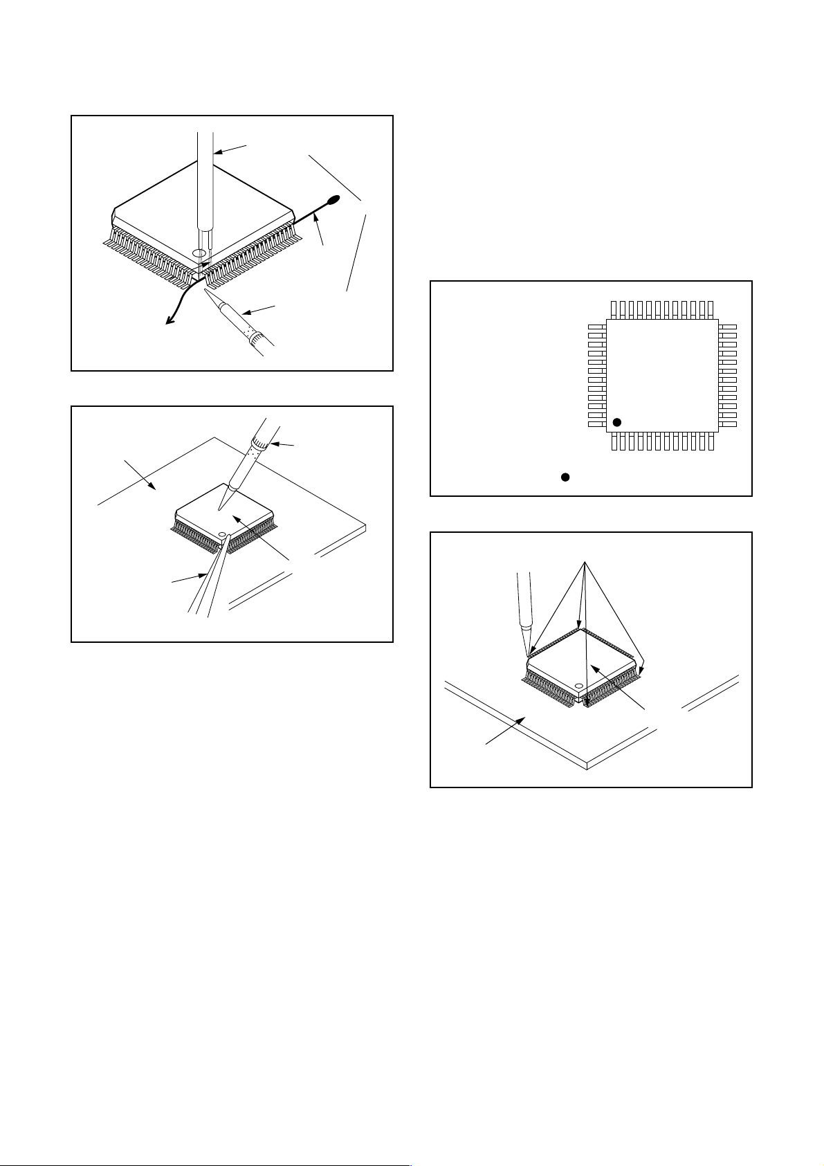
being held by glue. When the flat pack-IC is
removed from the CBA, handle it gently
because it may be damaged if force is applied.
Hot Air Blower
or
Iron Wire
2. Installation
1. Using desoldering braid, remove the solder from
the foil of each pin of the flat pack-IC on the CBA
so you can install a replacement flat pack-IC more
easily.
2. The “●” mark on the flat pack-IC indicates pin 1.
(See Fig. S-1-7.) Be sure this mark matches the 1
on the PCB when positioning for installation. Then
presolder the four corners of the flat pack-IC. (See
Fig. S-1-8.)
3. Solder all pins of the flat pack-IC. Be sure that
none of the pins have solder bridges.
To Solid
Mounting Point
CBA
Tweezers
Soldering Iron
Fig. S-1-5
Fine Tip
Soldering Iron
Flat Pack-IC
Fig. S-1-6
Example :
Pin 1 of the Flat Pack-IC
is indicated by a " " mark.
Presolder
Fig. S-1-7
CBA
Flat Pack-IC
Fig. S-1-8
1-3-4 TVVCRP_SN
Page 13
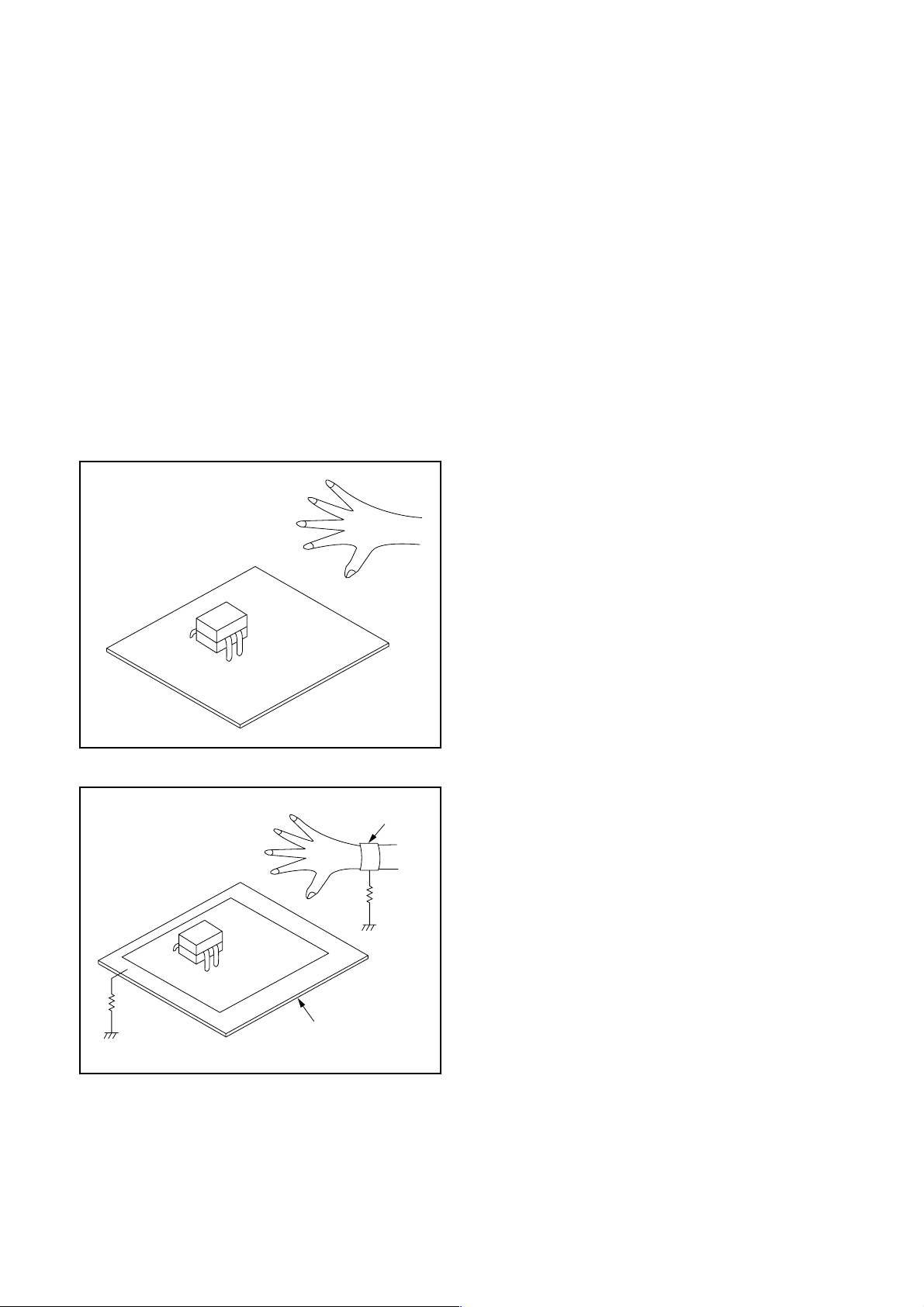
Instructions for Handling Semiconductors
Electrostatic breakdown of the semi-conductors may
occur due to a potential difference caused by
electrostatic charge during unpacking or repair work.
1. Ground for Human Body
Be sure to wear a grounding band (1 MΩ) that is
properly grounded to remove any static electricity that
may be charged on the body.
2. Ground for Workbench
Be sure to place a conductive sheet or copper plate
with proper grounding (1 MΩ) on the workbench or
other surface, where the semi-conductors are to be
placed. Because the static electricity charge on
clothing will not escape through the body grounding
band, be careful to avoid contacting semi-conductors
with your clothing.
<Incorrect>
<Correct>
1MΩ
CBA
Grounding Band
1MΩ
CBA
Conductive Sheet or
Copper Plate
1-3-5 TVVCRP_SN
Page 14
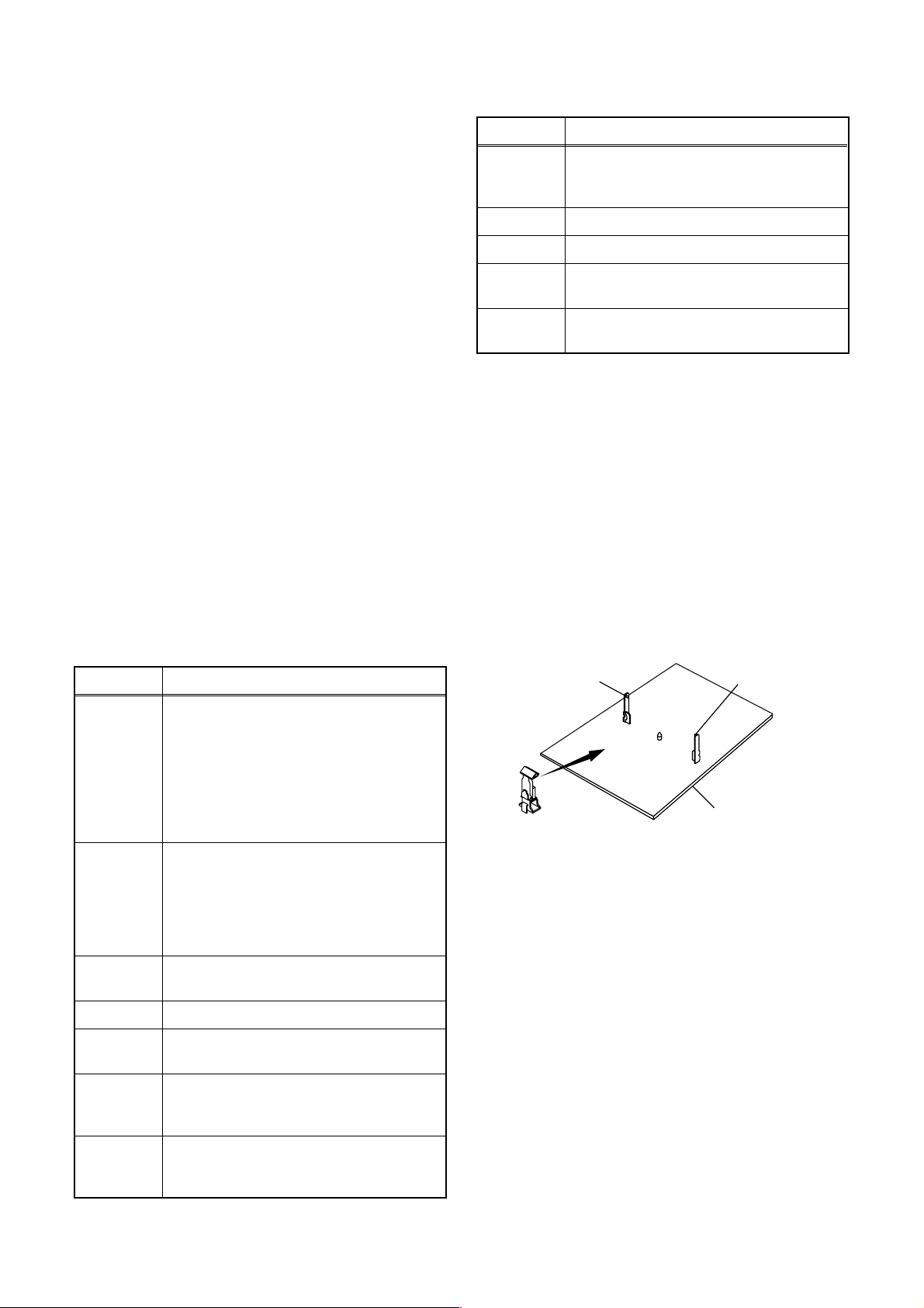
PREPARATION FOR SERVICING
How to Enter the Service Mode
Caution 1:
1. Optical sensors system are used for Tape Start
and End Sensor on this equipment. Read this
page carefully and prepare as described on this
page before starting to service; otherwise, the unit
may operate unexpectedly.
Preparing 1:
1. Cover Q202 (START SENSOR) and Q201 (END
SENSOR) with Insulation Tape or enter the
service mode to activate Sensor Inhibition
automatically.
Note: Avoid playing, rewinding or fast forwarding the
tape to its beginning or end, because both
Tape End Sensors are not active.
How to Enter the Service Mode
1. Turn the power on. (Use main power on the TV
unit.)
2. Press [STANDBY/ON], [2], [7], [1], and [MUTE]
buttons on the remote control unit in that order
within 5 seconds. When entering the service
mode, “4” will display at corners of the screen.
3. During the service mode, electrical adjustment
mode can be selected by remote control key.
Details are as follows.
Key Adjustment Mode
Key Adjustment Mode
Head switching position adjustment
5
6 No need to use.
7 No need to use.
8
9
Caution 2:
1. The deck mechanism assembly is mounted on the
Main CBA directly, and SW211 (REC-SAFETY
SW) is mounted on the Main CBA. When deck
mechanism assembly is removed from the Main
CBA due to servicing, this switch can not be
operated automatically.
(Manual adjustment): See adjustment
instructions page 1-6-7.
H. Shift adjustment: See adjustment
instructions page 1-6-4.
V. Size/V. Shift adjustment: See
adjustment instructions page 1-6-4.
Preparing 2:
1. To eject the tape, press the [STOP/EJECT] button
on the unit (or Remote Control).
2. When you want to record during the Service
mode, press the [Rec] button while depressing
SW211 (REC-SAFETY SW) on the Main CBA.
Q201
(END SENSOR)
Q202
(START SENSOR)
Picture adjustment mode: Press the
[MENU] button to change from BRT
(Bright), *CNT (Contrast), *COL (Color),
MENU
VOL-
0
1 No need to use.
2
3
4
*TNT(Tint) and SHP(SHARP). Press
[PROG+/PROG-] buttons to adjust
Initial Value.
*Marked items are not necessary to
adjust normally.
SECAM Black Level adjustment: See
adjustment instructions page 1-6-3.
Cut-off adjustment: See adjustment
instructions page 1-6-5.
White Balance adjustment: See
adjustment instructions page 1-6-5.
C-Trap adjustment: See adjustment
instructions page 1-6-3.
H adjustment mode: See adjustment
instructions page 1-6-2.
Head switching position adjustment
(Auto adjustment): See adjustment
instructions page 1-6-7.
Auto record mode: Perform recording
(15 Sec.)-->Stop-->Rewind (Zero
return) automatically.
SW211
(REC-SAFETY SW)
MAIN CBA
1-4-1 T6609PFS
Page 15
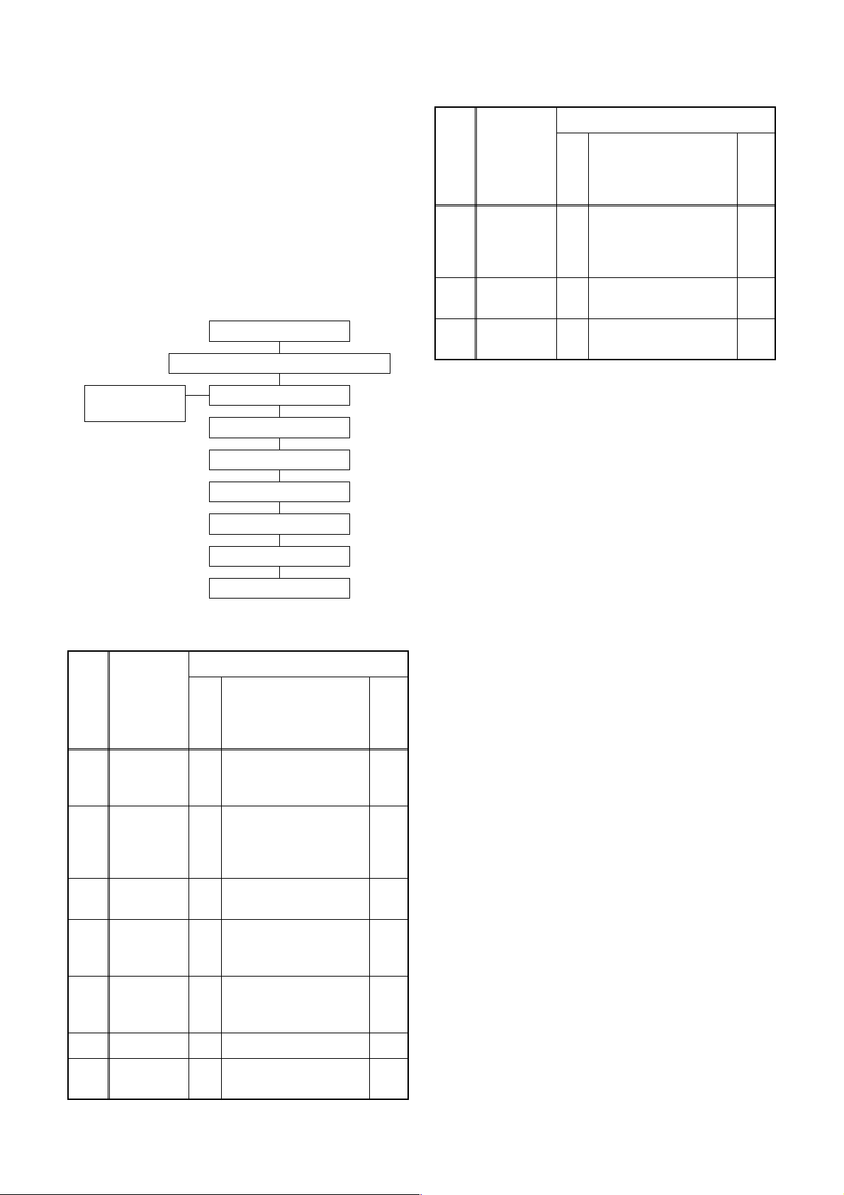
CABINET DISASSEMBLY INSTRUCTIONS
1. Disassembly Flowchart
This flowchart indicates the disassembly steps for the
cabinet parts and the CBA in order to gain access to
item(s) to be serviced. When reassembling, follow the
steps in reverse order. Bend, route and dress the
cables as they were.
CAUTION!
When removing the CRT, be sure to discharge the
Anode Lead of the CRT with the CRT Ground Wire
before removing the Anode Cap.
[1] Rear Cabinet
[2] Power Unit and Tray Chassis Unit
[3] Power Unit[5] H.V./Power
Supply CBA
[4] Tray Chassis Unit
[6] Top Cover
[7] Bottom Plate
[8] Deck Unit
[9] Main CBA
[10] CRT
2. Disassembly Method
Removal
Step/
Loc.
No.
[1]
[2]
[3] Power Unit
[4]
[5]
[6] Top Cover D3 5(S-4), *CL604 5
[7]
Part
Rear
Cabinet
Power Unit
and Tray
Chassis
Unit
Tr ay
Chassis
Unit
H.V./Power
Supply
CBA
Bottom
Plate
Remove/*Unhook/
Fig.
No.
D1
D2
D5
D3
D4
D5
D3D5*CN502, *CN552,
D3 ---------- ---
D3
D5
D3 (S-5) 6
Unlock/Release/
Unplug/Unclamp/
Desolder
4(S-1), 2(S-2),
*CN151
Anode Cap, *CN501,
*CN551, *CN601,
CRT CBA, Power
Knob
*CN602
6(S-3) 4
Note
1
2
3
Removal
Step/
Loc.
No.
[8] Deck Unit
[9] Main CBA
[10] CRT
↓
(1)
Note:
(1) Order of steps in procedure. When reassembling,
follow the steps in reverse order. These numbers
are also used as the Identification (location) No. of
parts in figures.
(2) Parts to be removed or installed.
(3) Fig. No. showing procedure of part location
(4) Identification of parts to be removed, unhooked,
unlocked, released, unplugged, unclamped, or
desoldered.
P = Spring, L = Locking Tab, S = Screw,
CN = Connector
* = Unhook, Unlock, Release, Unplug, or Desolder
e.g. 2(S-2) = two Screws (S-2),
2(L-2) = two Locking Tabs (L-2)
(5) Refer to the following “Reference Notes in the
Ta b le ” .
Part
↓
(2)
Remove/*Unhook/
Fig.
No.
D3
D5
D3
D5
D4
D5
(3)
Unlock/Release/
Unplug/Unclamp/
Desolder
7(S-6), (S-7), (S-8),
*Desolder (CN201,
CL401, CL402,
CL403)
4(S-9) 8
4(S-10) 9
↓
↓
(4)
Note
7
↓
(5)
Reference Notes in the Table
1. Removal of the Rear Cabinet.
Remove four screws (S-1) and two screws (S-2).
Disconnect connector CN151 and remove the
Rear Cabinet.
2. CAUTION!: Discharge the Anode Lead of the CRT
with the CRT Ground Wire before removing the
Anode Cap.
Removal of the Power Unit and Tray Chassis Unit.
Discharge the Anode Lead of the CRT with the
CRT Ground before removing the Anode Cap.
Disconnect the following: Anode Cap, CN501,
CN551, CN601, CRT CBA, and Power Button.
Then pull the Power Unit and Tray Chassis Unit out
backward.
3. Removal of the Power Unit.
Disconnect connectors CN502, CN552, and
CN602. Then slide the Power Unit out.
4. Removal of the H.V./Power Supply CBA.
Remove six screws (S-3) and pull up the H.V./
Power Supply CBA.
1-5-1 T6609DC
Page 16
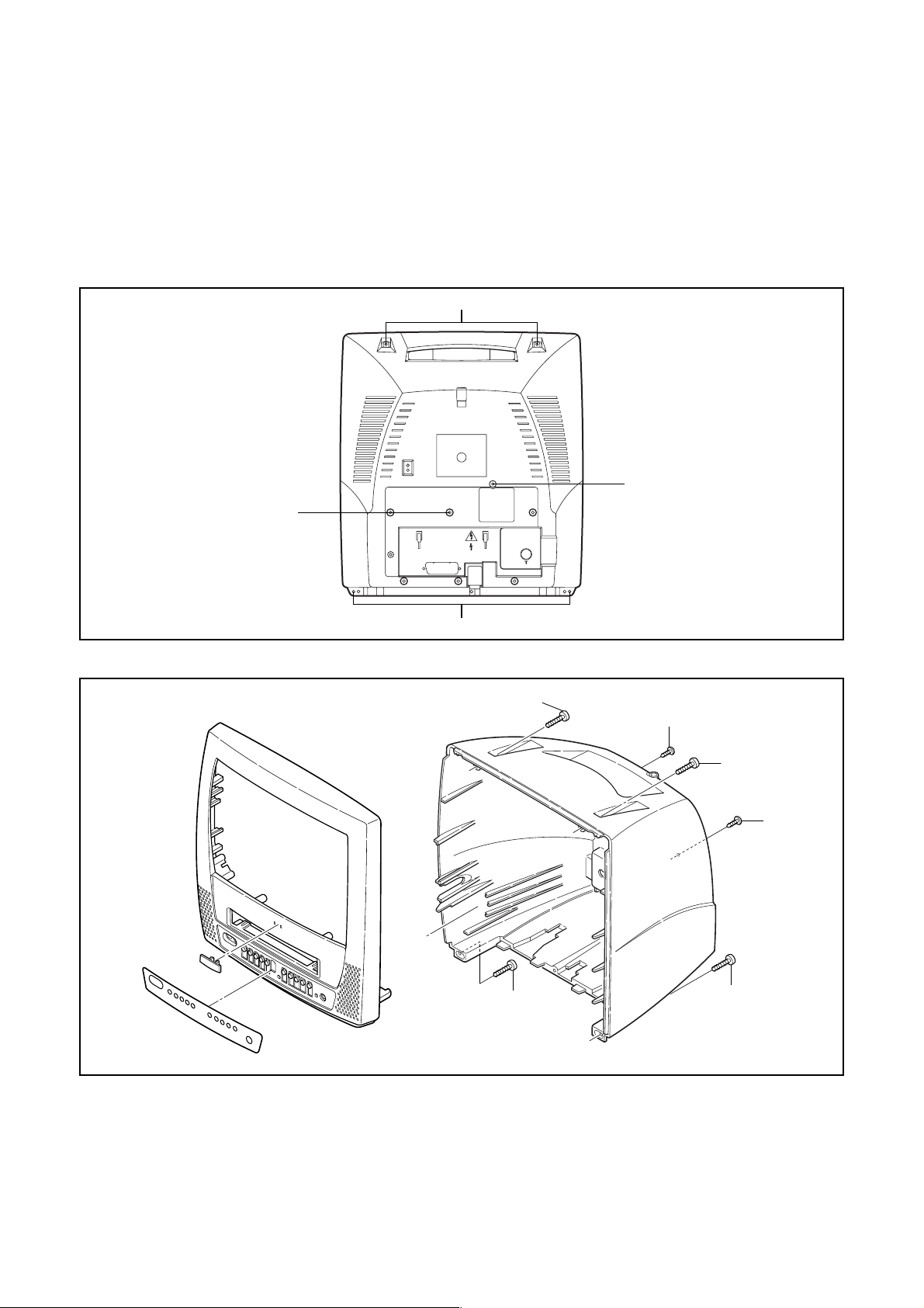
5. Removal of the Top Cover.
Remove five screws (S-4) and CL604, and remove
the Top Cover.
6. Removal of the Bottom Plate.
Remove a screw (S-5). Then slide the Bottom
Plate out front.
7. Removal of the Deck Unit.
Remove seven screws (S-6), screw (S-7) and
screw (S-8). Then, desolder connectors (CN201,
CL401, CL402, CL403) and lift up the Deck Unit.
(S-2)
8. Removal of the Main CBA.
Remove four screws (S-9) and pull up the Main
CBA.
9. Removal of the CRT.
Remove four screws (S-10) and pull the CRT
backward.
(S-1)
[1] Rear Cabinet
(S-2)
(S-1)
(S-1)
(S-1)
[1] Rear Cabinet
Fig. D1
(S-2)
(S-1)
(S-2)
(S-1)
Fig. D2
1-5-2 T6609DC
Page 17
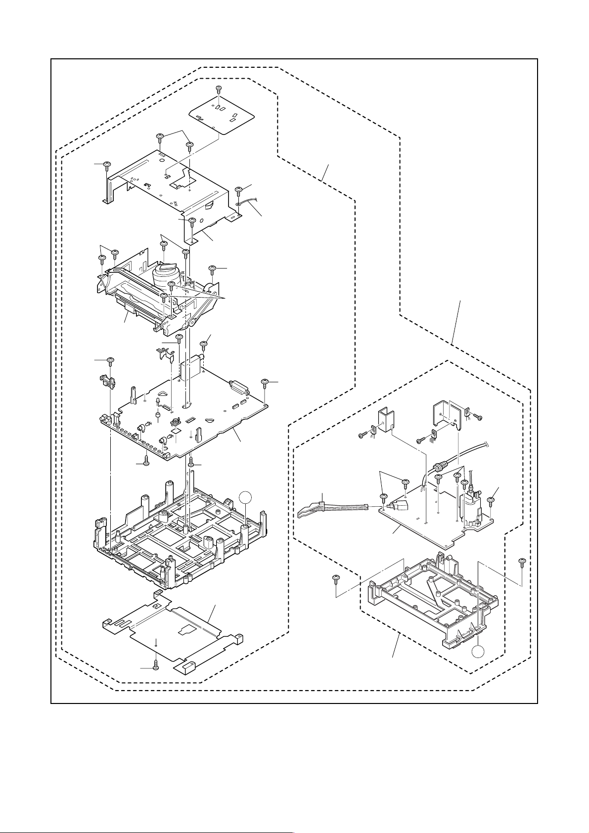
(S-4)
(S-4)
[4] Tray
Chassis Unit
(S-4)
(S-6)
[8] Deck Unit
(S-9)
(S-7)
(S-6)
(S-9)
(S-4)
[6] Top Cover
(S-6)
(S-6)
(S-9)
[9] Main CBA
(S-8)
A
CL604
(S-9)
Power Button
(S-3)
[2] Power Unit and
Tray Chassis Unit
(S-3)
(S-3)
(S-5)
[5] H.V./Power
Supply CBA
[7] Bottom Plate
A
[3] Power Unit
Fig. D3
1-5-3 T6609DC
Page 18
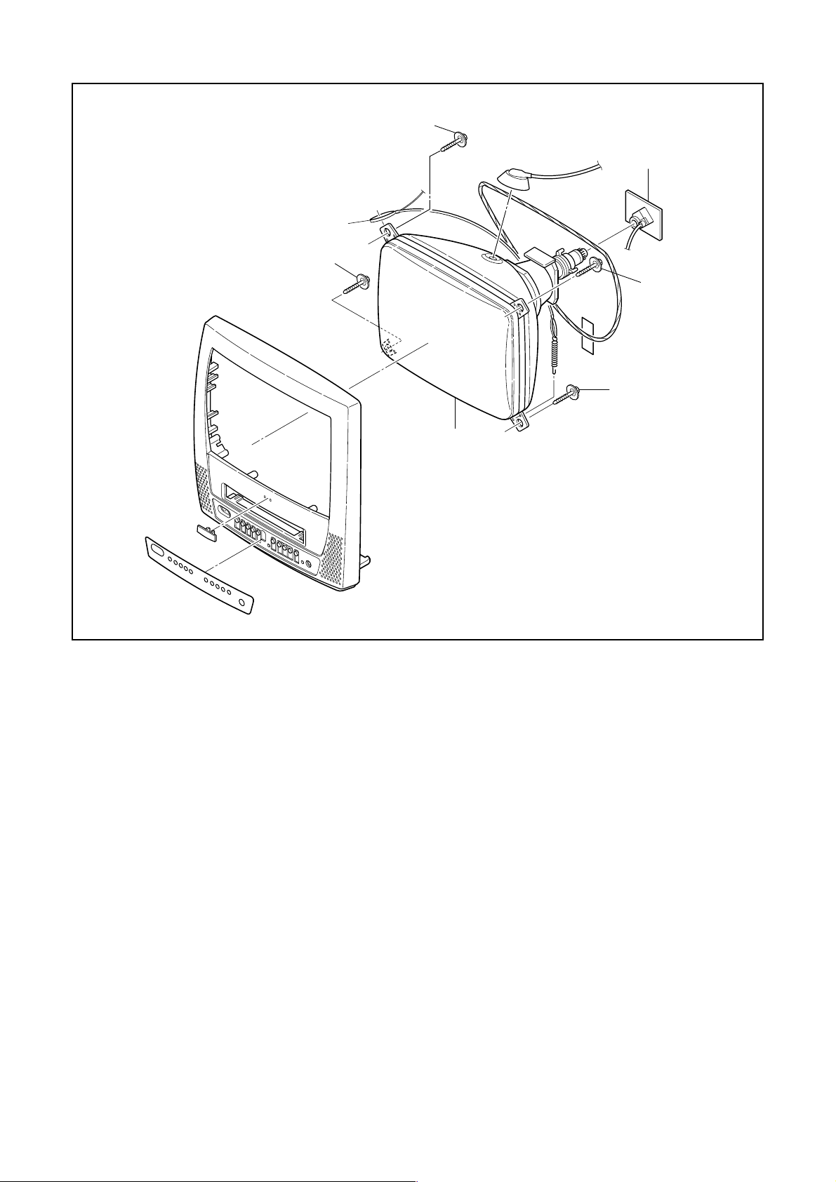
(S-10)
(S-10)
[10] CRT
Anode Cap
CRT CBA
(S-10)
(S-10)
Fig. D4
1-5-4 T6609DC
Page 19
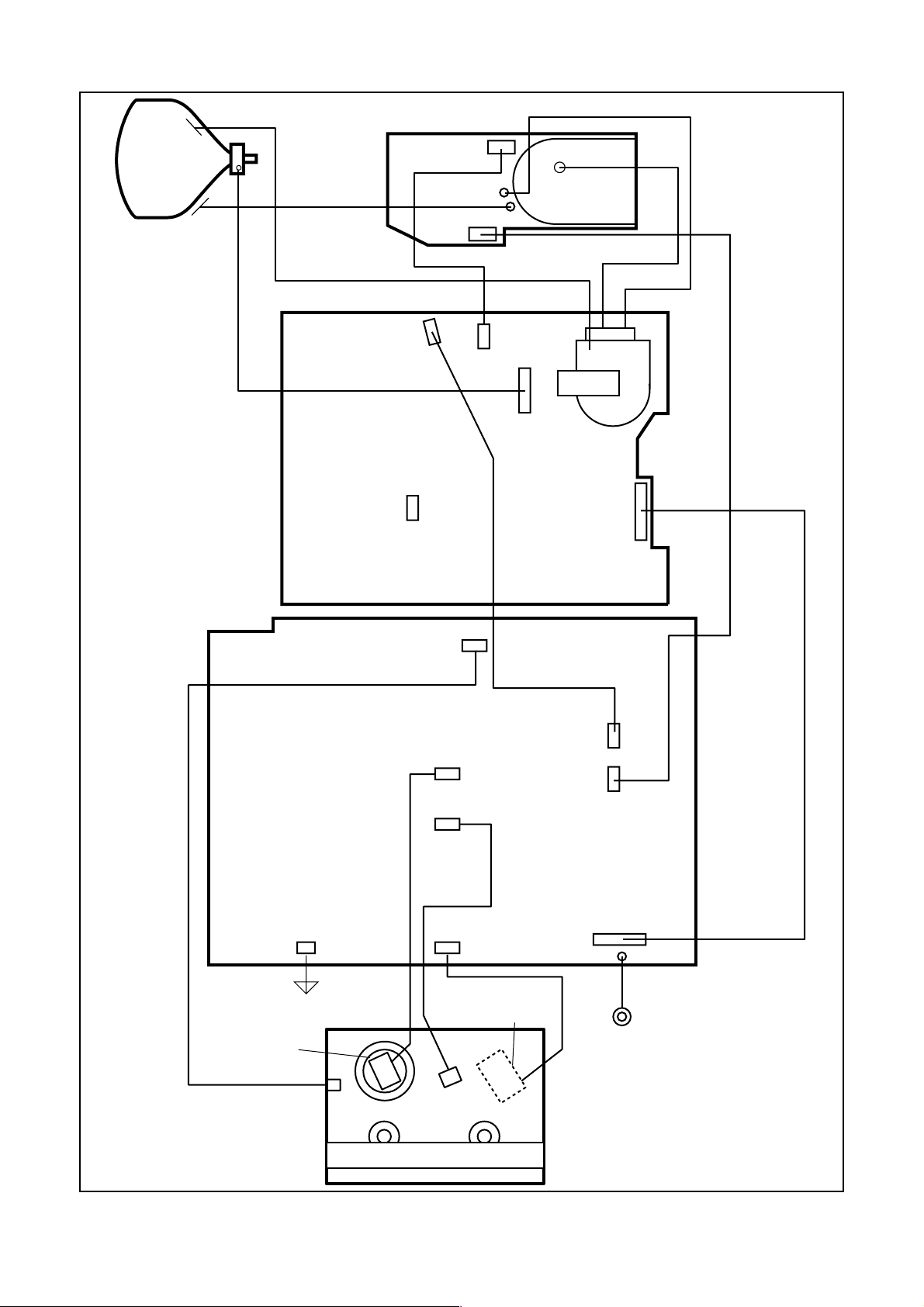
ANODE
CRT
GND
CRT CBA
CN501B
SCREEN
CN502
H.V./POWER SUPPLY CBA
CN552
CL501A
FOCUS
CN501
CN551
MAIN CBA
CN151
CN601
TO DEGAUSS
COIL
CL403
CL401
CL402
CN201
CN602
CL302A
CL301A
CL603A
TO SPEAKER
CYLINDER
ASSEMBLY
FE HEAD
CAPSTAN
ACE HEAD
ASSEMBLY
MOTOR
TO TOP COVER
DECK UNIT
CL604
1-5-5 T6609DC
Fig. D5
Page 20

ELECTRICAL ADJUSTMENT INSTRUCTIONS
General Note: “CBA” is abbreviation for
“Circuit Board Assembly.”
Note: Electrical adjustments are required after
replacing circuit components and certain
mechanical parts. It is important to perform
these adjustments only after all repairs and
replacements have been completed.
Also, do not attempt these adjustments unless
the proper equipment is available.
Test Equipment Required
1. PAL Pattern Generator (Color Bar, Monoscope,
Black Raster, White Raster, Sympte)
2. SECAM Pattern Generator (Gray Scale)
3. AC Milli Voltmeter (RMS)
4. Alignment Tape (FL6A), Blank Tape (E180)
5. DC Voltmeter
6. Oscilloscope: Dual-trace with 10:1 probe,
V-Range: 0.001~50 V/Div,
F-Range: DC~AC-60 MHz
7. Frequency Counter
8. Plastic Tip Driver
9. RF input (at each broadcasting system)
Receiving Channel: VHF Low
Input level: 80dBµV
10. Ext.input
FRONT VIDEO-IN JACK or REAR SCART JACK
How to Set up the Service mode:
Note: After replacing the IC202 (Memory) or Main
CBA, the set value in IC202 (Memory) will be
lost. So it is necessary to set up or adjust in
the Service mode after its replacement.
Service Mode:
1. Turn the power on. (Use main power on the TV
unit.)
2. Press [STANDBY/ON], [2], [7], [1], and [MUTE]
buttons on the remote control unit in that order
within 5 seconds.
- To cancel the Service mode, press [STANDBY/
ON] button on the remote control.
How to Set up the Option Code
1. Enter the Service mode.
2. Press the [STATUS] button on the remote control
unit. The option code appears on the display.
3. If needed, input the option code (0128) using
number buttons on the remote control unit.
4. To reset the software, press [PAUSE] and [5]
buttons on the remote control unit.
The option code is changed.
1-6-1 T6609EA
Page 21

1. DC 105V (+B) Adjustment
2. H Adjustment
Purpose: To obtain correct operation.
Symptom of Misadjustment: The picture is dark and
unit does not operate correctly.
Test Point Adj. Point Mode Input
TP503(+B),
TP504(GND)
Tape M. E Q . Sp e c.
---
Note: TP503(+B), TP504(GND),
VR601 --- H.V./Power Supply CBA
1. Connect the unit to AC Power Outlet. (exact AC
230 V)
2. Input a color bar signal from RF (or Ext.) input and
leave it for at least 20 minutes.
3. Connect DC Volt Meter to TP503(+B) and
TP504(GND).
4. Adjust VR601 so that the voltage of TP503(+B)
becomes +105±0.5 V DC.
VR601
DC Voltmeter,
Plastic Tip Driver
RF
(or Ext.)
+105±0.5 V DC
Color
Bar
Purpose: To get correct horizontal position and size of
screen image.
Symptom of Misadjustment: Horizontal position and
size of screen image may not be properly displayed.
Test Point Adj. Point Mode Input
R590
Tape M. EQ. Spec.
--- Frequency Counter 15.625 kHz±250 Hz
Note: R590 --- H.V./Power Supply CBA
1. Connect Frequency Counter to R590.
2. Set the unit to the Ext. mode and no input is
necessary. Enter the Service mode.
(See page 1-6-1.)
3. Operate the unit for at least 20 minutes.
4. Press [2] button on the remote control unit and
select H-Adj mode.
5. Press [PROG+/PROG-] buttons on the remote
control unit so that the display will change “0” to
“7.”
At this moment, choose display “0” to “7” when the
Frequency counter display is closest to 15.625
kHz ± 250 Hz.
6. Turn the power off and on again.
[PROG+/PROG-]
buttons
Ext. ---
1-6-2 T6609EA
Page 22
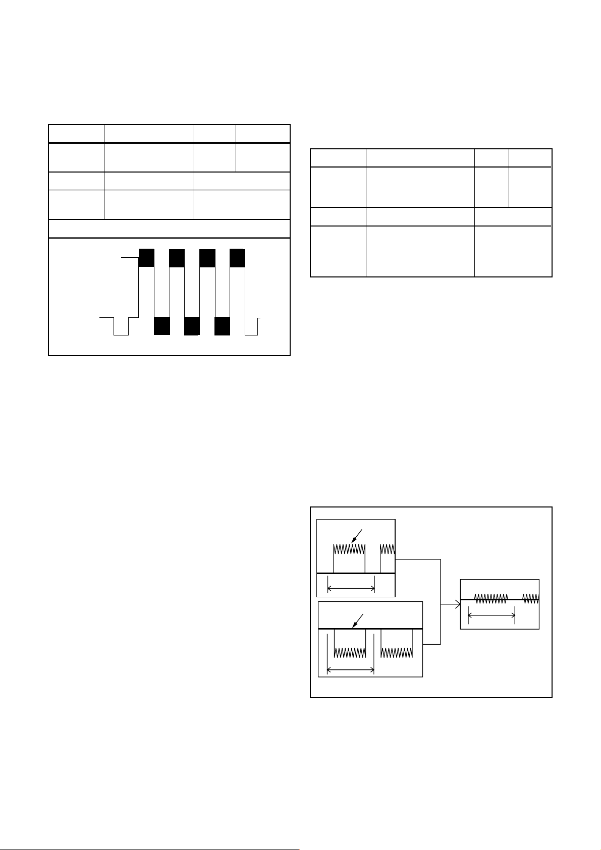
3. C-Trap Adjustment
4. SECAM Black Level Adjustment
Purpose: To get minimum leakage of the color signal
carrier.
Symptom of Misadjustment: If C-Trap Adjustment is
incorrect, stripes will appear on the screen.
Test Point Adj. Point Mode Input
J349F3
(B-OUT)
Tape M. EQ. Spec.
---
[PROG+/PROG-]
buttons
Oscilloscope,
Pattern Generator
Figure
RF
(or Ext.)
200 mVp-p Max.
Color Bar
minimum
Fig. 1
Note: J349F3(B-OIT) --- Main CBA
1. Connect Oscilloscope to J349F3.
2. Input a color bar signal from RF (or Ext.) input.
Enter the Service mode. (See page 1-6-1.)
3. Press [0] button on the remote control unit and
select C-TRAP mode.
4. Press [PROG+/PROG-] buttons on the remote
control unit so that the carrier leakage B-Out (4.43
MHz) value becomes minimum on the
oscilloscope.
5. Turn the power off and on again.
Purpose: To set Black Level of the SECAM signal RY/B-Y to Ref. level.
Symptom of Misadjustment: If Black Level of the
SECAM signal R-Y/B-Y is incorrect, the picture is
bluish or reddish in grayscale compared with PAL
signal.
Test Point Adj. Point Mode Input
J361G4
Tape M. EQ. Spec.
---
Note: J361G4 --- Main CBA
1. Degauss the CRT and allow CRT to operate for 20
minutes before starting the alignment.
2. Input the SECAM Gray Scale signal from Ext.
input.
3. Enter the Service mode. (See page 1-6-1.)
4. To enter the C/D/S mode, press [VOL-] button on
the remote control unit.
5. To select SBR (SECAM Black Level R-Y), press
[6] button on the remote control unit.
6. Press [PROG+/PROG-] buttons to adjust Y signal
to the black ref. level.
7. To select SBB (SECAM Black Level B-Y), press [7]
button on the remote control unit.
8. Press [PROG+/PROG-] buttons to adjust Y signal
to the black ref. level.
[PROG+/PROG-]
buttons
Pattern Generator,
Analog Oscilloscope
(unusable Digital
Oscilloscope)
Ext.
SECAM
Gray
Scale
---
Y Signal
1H
Black REF. Level
1H
1H
5 mV/Div (10:1 Prove)
Fig. 2
1-6-3 T6609EA
Page 23
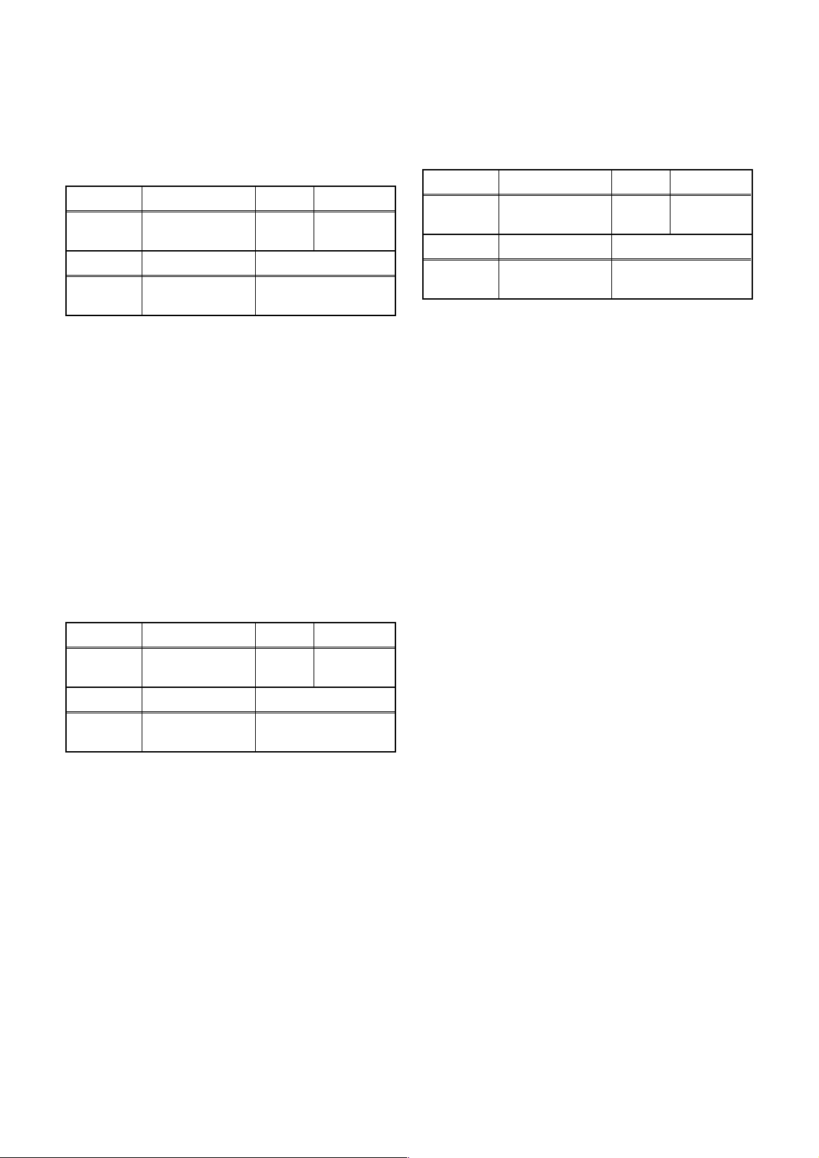
5. V. Size Adjustment
7. H. Shift Adjustment
Purpose: To obtain correct vertical height of screen
image.
Symptom of Misadjustment: If V. Size is incorrect,
vertical height of image on the screen may not be
properly displayed.
Test Point Adj. Point Mode Input
Screen
Tape M. EQ. Spec.
---
1. Enter the Service mode. (See page 1-6-1.)
Press [9] button on the remote control unit and
select V-S mode. (Press [9] button then display will
change to V-P and V-S).
2. Input monoscope pattern and leave it for at least
20 minutes.
3. Press [PROG+/PROG-] buttons on the remote
control unit so that the monoscope pattern is
90±5% of display size and the circle is round.
[PROG+/PROG-]
buttons
Pattern
Generator
RF
(or Ext.)
Monoscope
90±5%
Purpose: To obtain correct horizontal position and
size of screen image.
Symptom of Misadjustment: Horizontal position and
size of screen image may not be properly displayed.
Test Point Adj. Point Mode Input
Screen
Tape M. EQ. Spec.
---
1. Enter the Service mode. (See page 1-6-1.)
Press [8] button on the remote control unit and
select H-P mode.
2. Input monoscope pattern and leave it for at least
20 minutes.
3. Press [PROG+/PROG-] buttons on the remote
control unit so that the left and right side of the
monoscope pattern are equal to each other.
4. Turn the power off and on again.
[PROG+/PROG-]
buttons
Pattern
Generator
RF
(or Ext.)
Monoscope
90±5%
6. V. Shift Adjustment
Purpose: To obtain correct vertical position of screen
image.
Symptom of Misadjustment: If V. position is
incorrect, vertical position of image on the screen may
not be properly displayed.
Test Point Adj. Point Mode Input
Screen
Tape M. EQ. Spec.
---
1. Enter the Service mode. (See page 1-6-1.)
Press [9] button on the remote control unit and
select V-P mode. (Press [9] button then display will
change to V-P and V-S).
2. Input monoscope pattern and leave it for at least
20 minutes.
3. Press [PROG+/PROG-] buttons on the remote
control unit so that the top and bottom of the
monoscope pattern are equal to each other.
[PROG+/PROG-]
buttons
Pattern
Generator
RF
(or Ext.)
Monoscope
90±5%
1-6-4 T6609EA
Page 24
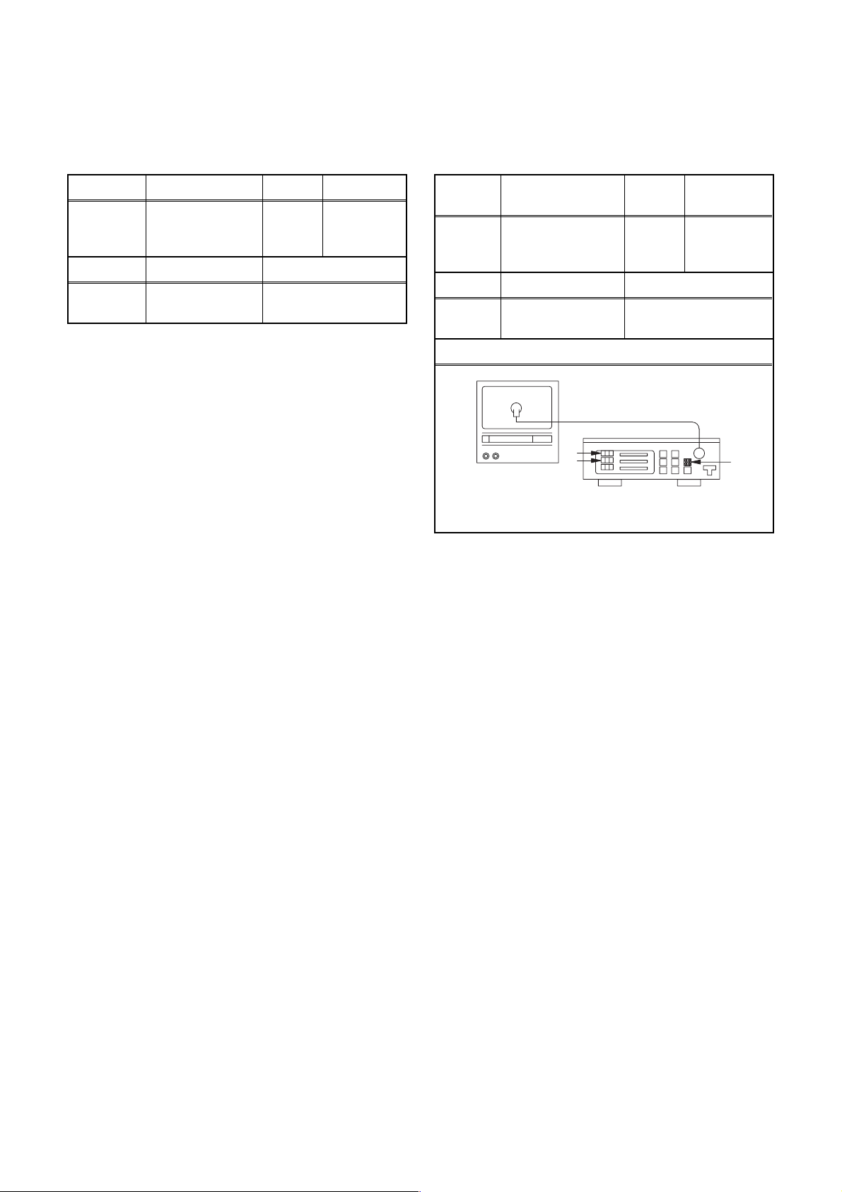
8. Cut-off Adjustment
9. White Balance Adjustment
Purpose: To adjust the beam current of R, G, B, and
screen voltage.
Symptom of Misadjustment: White color may be
reddish, greenish or bluish.
Test Point Adj. Point Mode Input
Screen-Control,
Screen
Tape M. EQ. Spec.
---
Note: Screen Control (FBT) --- H.V./Power Supply
1. Degauss the CRT and allow CRT to operate for 20
minutes before starting the alignment.
2. Set the screen control to minimum position. Input
the Black raster signal from RF (or Ext.) input.
3. Enter the Service mode. (See page 1-6-1.)
Dimmed horizontal line appears on the CRT.
4. To enter the C/D/S mode, press the [VOL-] button
on the remote control unit.
5. To enter the CUT OFF (R) mode, press [1] button
on the remote control unit.
6. Turn the screen control up until dimmed horizontal
line appears.
7. Press the [PROG+/PROG-] buttons until the
horizontal line becomes white.
8. To enter the CUT OFF (G) mode, press [2] button
on the remote control unit.
9. Press the [PROG+/PROG-] buttons until the
horizontal line becomes white.
10. To enter the CUT OFF (B) mode, press [3] button
on the remote control unit.
11. Press the [PROG+/PROG-] buttons until the
horizontal line becomes white.
12. Turn the screen control so that the horizontal line
adjusted white looks lightly.
13. Turn the power off and on again.
[PROG+/PROG-]
buttons
Pattern
Generator
CBA
FBT= Fly Back Transformer
Use the Remote Control Unit
RF
(or Ext.)
See Reference Notes
Black
Raster
below
Purpose: To mix red, green and blue beams correctly
for pure white.
Symptom of Misadjustment: White becomes bluish
or reddish.
Tes t
Point
Screen
Tape M. EQ. Spec.
---
Note: Use remote control unit
1. Operate the unit more than 20 minutes.
2. Face the unit to east. Degauss the CRT using
Degaussing Coil.
3. Input the White Raster (APL 100%).
4. Set the color analyzer to the CHROMA mode and
after zero point calibration, bring the optical
receptor to the center on the tube surface (CRT).
5. Enter the Service mode. Press [VOL-] button on
the remote control.
6. Press [4] button on the remote control unit for Red
adjustment. Press [5] button on the remote control
unit for Blue adjustment.
7. In each color mode, Press [PROG+/PROG-]
buttons to adjust the values of color.
8. Adjusting Red and Blue color so that the
temperature becomes 8500K (x: 290 / y: 300)
±3%.
9. At this time, Re-check that Horizontal line is white.
If not, Re-adjust Cut-off Adjustment until the
Horizontal Line becomes pure white.
10. Turn off and on again to return to normal mode.
Receive APL 100% white signal and Check
Chroma temperatures become 8500K (x: 290 / y:
300) ±3%.
Note: Confirm that Cut Off Adj. is correct after this
adjustment, and attempt Cut Off Adj. if
needed.
Adj. Point Mode Input
Screen-Control,
[PROG+/PROG-]
buttons
Pattern Generator,
Color analyzer
Figure
RF
(or Ext.)
See below
Color Ajalyzer
White
Raster
(APL 100%)
Fig. 3
1-6-5 T6609EA
Page 25
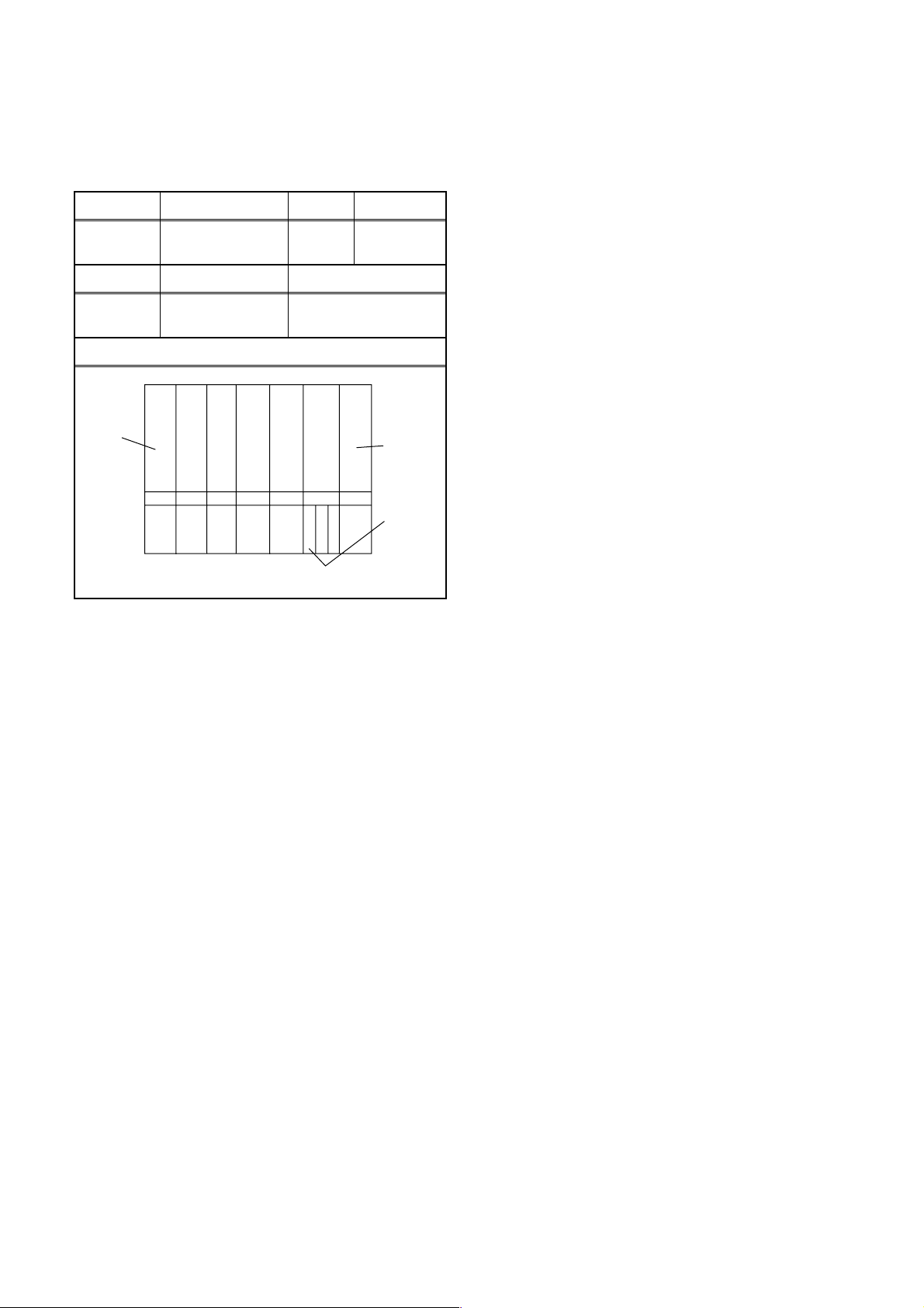
10. Sub-Brightness Adjustment
Purpose: To get proper brightness.
11. Setting for CONTRAST, COLOR,
TINT and SHARP Data Values
Symptom of Misadjustment: If Sub-Brightness is
incorrect, proper brightness cannot be obtained by
adjusting the Brightness Control.
Test Point Adj. Point Mode Input
Screen
Tape M. EQ. Spec.
---
White
Note: Bar (A) in Fig. 4 --- 0 IRE
1. Enter the Service mode. (See page 1-6-1.)
Then input SYMPTE signal from RF (or Ext.) input
and leave it for at least 20 minutes.
2. Press [MENU] button. (Each time [MENU] button
is pressed, display will change BRT, CNT, COL,
TNT, and SHP in that order.) Select BRT and
press [PROG+/PROG-] buttons so that the bar (A)
in Fig. 4 is just visible.
3. Turn the power off and on again.
[PROG+/PROG-]
buttons
Pattern
Generator
Figure
RF
(or Ext.)
See below
ABC
SYMPTE
Black
This bar
(A) just
visible
Fig. 4
General
1. Enter the Service mode. (See page 1-6-1.)
2. Press [MENU] button. (Each time [MENU] button
is pressed, display will change BRT, CNT, COL,
TNT, and SHP in that order.)
CONTRAST (CNT)
1. Press [MENU] button on the remote control unit.
Then select CNT display.
2. Press [PROG+/PROG-] buttons on the remote
control unit so that the value of “CONTRAST”
(CNT) becomes 83.
COLOR (COL)
1. Press [MENU] button on the remote control unit.
Then select “COLOR” (COL) display.
2. Press [PROG+/PROG-] buttons on the remote
control unit so that the value of “COLOR” (COL)
becomes 65.
TINT (TNT)
1. Press [MENU] button on the remote control unit.
Then select “TINT” (TNT) display.
2. Press [PROG+/PROG-] buttons on the remote
control unit so that the value of “TINT” (TNT)
becomes 68.
SHARP (SHP)
1. Press [MENU] button on the remote control unit.
Then select “SHARP” (SHP) display.
2. Press [PROG+/PROG-] buttons on the remote
control unit and select “1.”
1-6-6 T6609EA
Page 26
12. Focus Adjustment
Purpose: Set the optimum Focus.
13. Head Switching Position
Adjustment
Symptom of Misadjustment: If Focus Adjustment is
incorrect, blurred images are shown on the display.
Test Point Adj. Point Mode Input
Screen Focus Control
Tape M. EQ. Spec.
---
Note: Focus VR (FBT) --- H.V./Power Supply CBA
FBT = Fly Back Transformer
1. Operate the unit more than 30 minutes.
2. Face the unit to the East and degauss the CRT
using a Degaussing Coil.
3. Input the monoscope pattern.
4. Adjust the Focus Control on the FBT to obtain
clear picture.
Pattern
Generator
RF
(or Ext.)
See below.
Monoscope
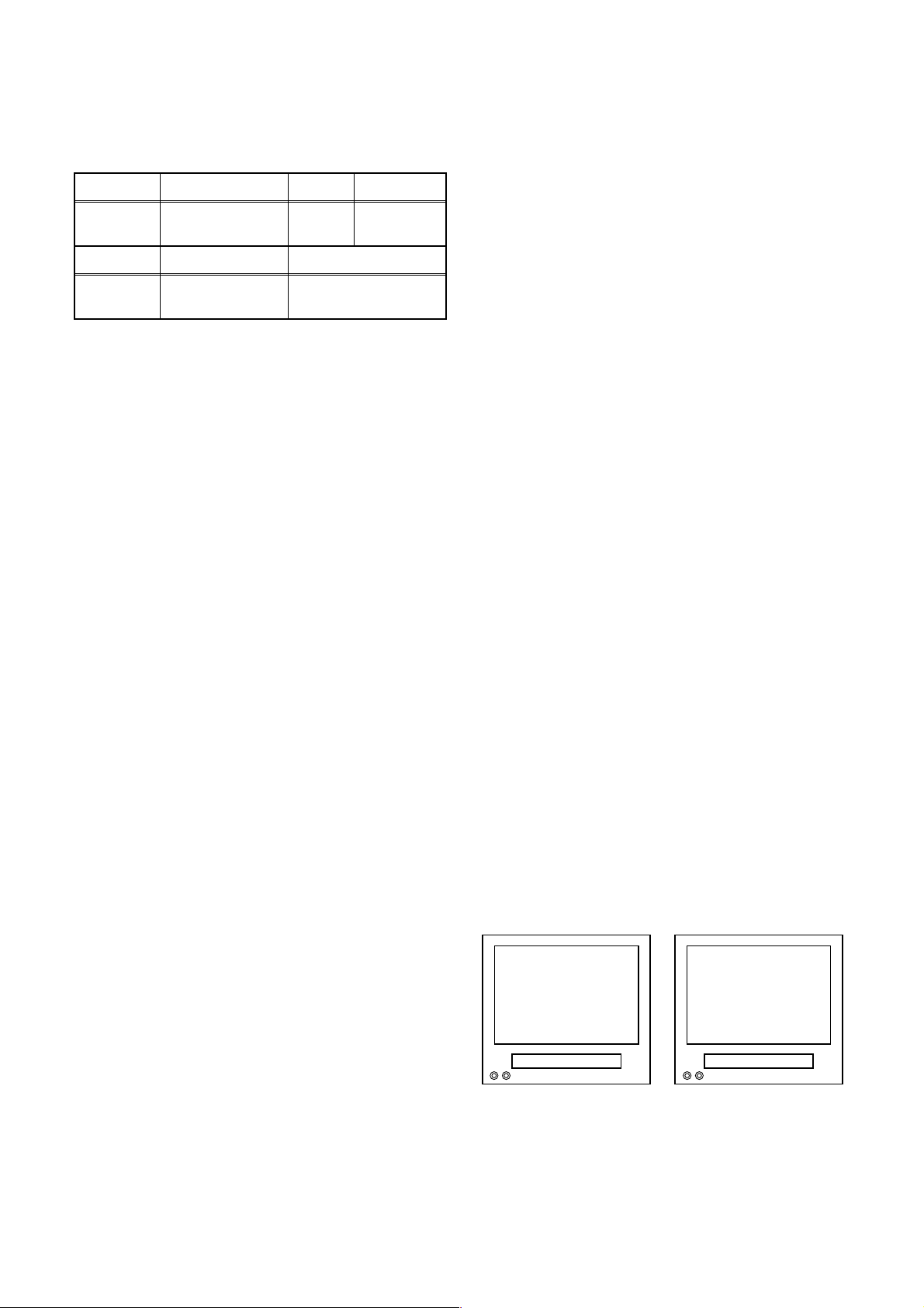
Purpose: Determine the Head Switching Position
during Playback.
Symptom of Misadjustment: May cause Head
Switching Noise or Vertical Jitter in the picture.
Note: Unit reads Head Switching Position
automatically and displays it on the screen
(Upper Left Corner).
Manual Adjustment
1. Enter the Service mode. (See page 1-6-1.)
2. Playback the test tape (FL6A).
3. Press the number [5] button on the remote control
unit.
4. The Head Switching position will display on the
screen; if adjustment is necessary follow step 4.
7.0H (448 µs) is preferable.
5. Press [PROG+/PROG-] buttons on the remote
control unit if necessary. The value will be
changed in 0.5H steps up or down. Adjustable
range is up to 9.5H. If the value is beyond
adjustable range, the display will change as:
Lower out of range: 0.0H
Upper out of range: -.-H
6. Turn the power off and on again.
Auto Adjustment
1. Load the test tape (FL6A) that have been recorded
the Head Switching Position Value.
2. Enter the Service mode. (See page 1-6-1.)
3. Press [3] button on the remote control unit in the
tape stop mode. The unit playback and adjust the
Head Switching Position automatically.
4. The adjusting report appears on upper left corner
of the screen with blueback.
In case of adjusting correctly: the Head Switching
Position Value recorded in the test tape (FL6A) is
indicated with green.
In case of adjusting incorrectly: “NG” (red) is
indicated with ejecting tape.
TVCR TVCR
7.0H
NG
Correct
1-6-7 T6609EA
Incorrect
Fig. 5
Page 27

HOW TO INITIALIZE THE TV/VCR COMBINATION
To put the program back at the factory-default,
initialize the TV/VCR Combination as the following
procedure.
1. Turn the power on. (Use main power on the TV
unit.)
2. To enter the Service mode, press [STANDBY/ON],
[2], [7], [1], and [MUTE] buttons on the remote
control unit in that order within 5 seconds.
- To cancel the Service mode, press [STANDBY/
ON] button on the remote control.
3. Press [SLEEP] button on the remote control unit to
start initializing.
- During initializing, OSD indication (digit) on the
four corners on TV screen blinks to white.
- After initializing, OSD indication lights to red.
4. Turn the power off by pressing main power button
on the TV unit, and unplug the AC cord from the
AC outlet.
1-7-1 T6609INT
Page 28
MECHANICAL TROUBLE INDICATOR
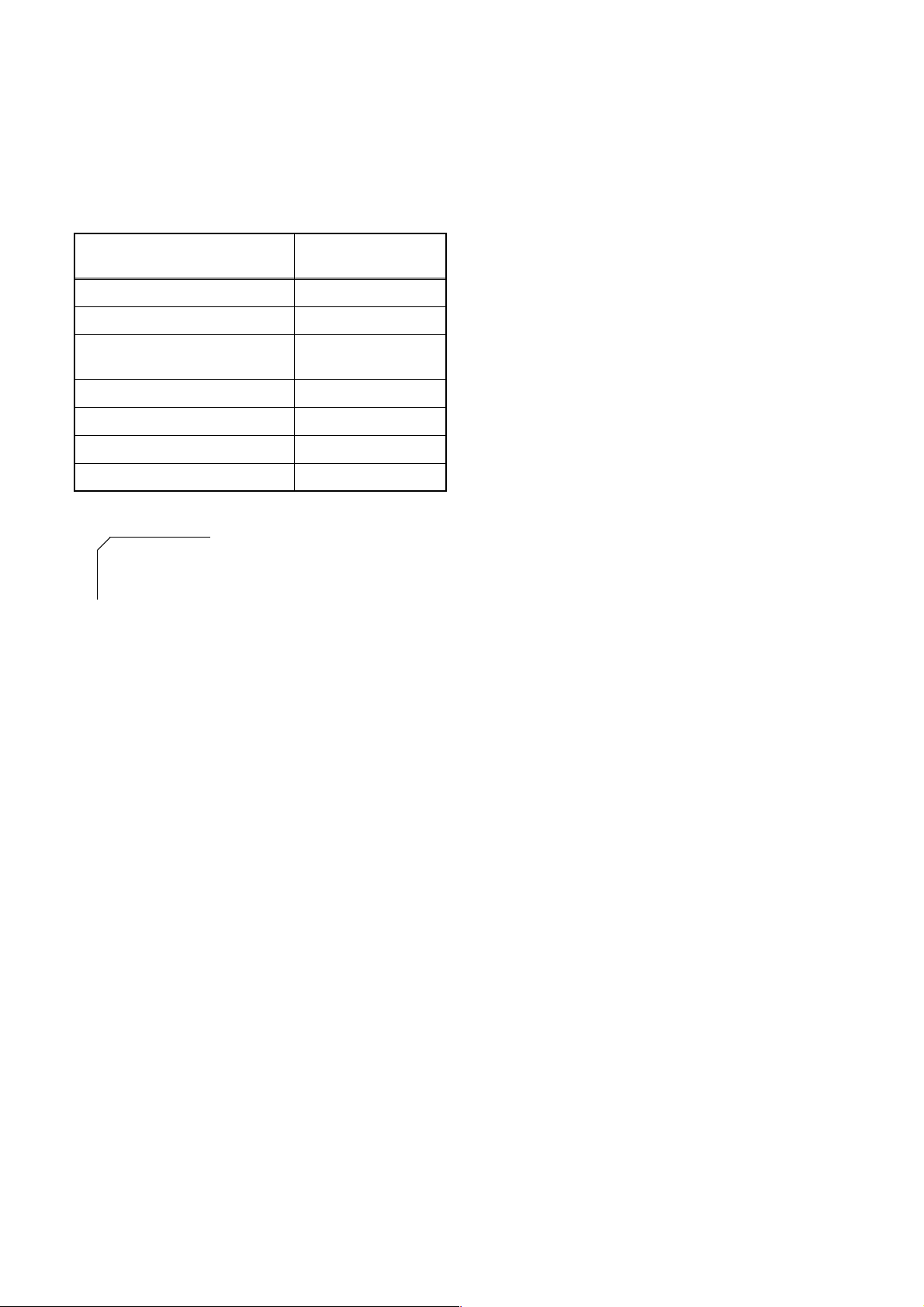
1. Each Malfunction Indication
If the MONITOR is turned ON right after the
Mechanical Malfunction occurs or POWER SAFETY/
X-RAY is turned ON, display the following character to
show Malfunction after the EJECT display.
Immediately preceding
Malfunction
REEL Malfunction R
DRUM Malfunction D
CASSETTE LOADING
Malfunction
TAPE LOADING Malfunction T
P-SAFETY 1 1
P-SAFETY 2 2
X-RAY X
Example: If REEL Malfunction
EJECT R
Display character
C
2. Each Malfunction evaluation
method
X-RAY protect
POWER SAFETY
POWER SAFETY 1
If P-SAFETY 1 port becomes continuously 2.5 V or
less for 120 msec. (4 times 40 msec. interval) when
MONITOR is ON, the unit shall be assumed to be the
Power Malfunction 1 and immediately turn OFF the
POWER/MONITOR and switch over the Mechanical
Malfunction mode with POWER OFF.
(To return from this mode shall become possible only
by POWER Key as in the case of the Mechanical
Malfunction).
* However the POWER SAFETY 1 function shall be
disabled during 500 msec. right after the MONITOR
turns ON.
POWER SAFETY 2
If P-SAFETY 2 port becomes continuously 2.5 V or
less for 120 msec. (4 times 40 msec. interval) when PON-H port is ON, the unit shall be assumed to be the
Power Malfunction 2 and immediately turn OFF the
POWER/MONITOR and switch over the Mechanical
Malfunction mode with POWER OFF.
(To return from this mode shall become possible only
by POWER Key as in the case of the Mechanical
Malfunction).
* However the POWER SAFETY 2 function shall be
disabled during 500 msec. right after the P-ON-H port
turns ON.
If X-RAY port becomes continuously 2.5 V or more for
120 msec. (4 times 40 msec. interval), the unit shall
immediately turn OFF the POWER/MONITOR and
switch over to the Mechanical Malfunction mode with
POWER OFF.
(To return from this mode shall become possible only
by POWER Key as in the case of the Mechanical
Malfunction).
1-8-1 T6609MTI
Page 29

Mechanical Malfunction determination
1. REEL Malfunction detection
Countermeasure for REEL and CAPSTAN motor
rotation malfunction (Except CASSETTE
LOADING function)
After the Malfunction detection with REEL/CAPSTAN sensor, the unit shall switch over to STOP
(B) and be REEL Mechanical Malfunction.
a. If the T-REEL pulse is not impressed after a
lapse of 7 sec. at SP, 14 sec. at LP, or more in
the REEL Rotation Mode like PLAY/REC, FS/
RS Mode, and the T-REEL or S-REEL pulse is
not impress after a lapse of 4 sec. or more in
REEL Rotation Mode of FF/REW, it shall be
assumed to stop the rotation and switch over to
STOP (B) position, then POWER be turned
OFF and the unit be REEL Mechanical
Malfunction. (T-REEL and S-REEL for the
models on S-REEL and only T-REEL for other
models)
b. If the C-FG pulse is not impressed for a lapse
of 1 sec. or more during the CAPSTAN MOTOR
rotation, it shall be MOTOR Rotation
Malfunction (REEL Malfunction).
2. DRUM Malfunction detection
Detect the DRUM rotation at the D-FG input
terminal.
If the variation of D-FG input level is not detected
for a lapse of 1 sec. or more when D-CONT is “H”,
it shall be assumed to be Rotation Malfunction and
be DRUM Malfunction.
When detect Drum Malfunction, POWER shall be
turned OFF after the unit switches over to STOP
(B) Mode.
3. Countermeasure for TAPE LOADING Malfunction
Detect the Malfunction with the LOADING Switch.
a. TAPE LOADING Malfunction
If LD-SW does not go to the established
position after a lapse of 7 sec. or more from
TAPE LOADING or TAPE UNLOADING start,
the LOADING function shall immediately be
stopped and POWER be turned OFF, and
inform the Timer about the LOADING
Mechanical Malfunction.
b. LD-SW Position Malfunction at each mode
When the unit operates at each mode, even if
the LD-SW position changes from the
established one in its mode, it keeps the
function according to its mode.
4. Countermeasure for CASSETTE LOADING
Malfunction
a. CASSETTE IN operating Malfunction
If LD-SW does not go to SB position after a
lapse of 5 sec. or more from the CASSETTE
insertion start, the unit starts the CASSETTE
OUT operation.
After switch over to CASSETTE OUT operation
and then a laps of 5 sec. or more from the
CASSETTE OUT operation start, if LD-SW
does not go to the EJ position or if START
Sensor and END Sensor does not turn “ON” at
the EJ position, the unit starts again to insert
CASSETTE.
(However in S-INH state, the START/END
Sensor shall be disabled).
b. CASSETTE OUT operating Malfunction
After a lapse of 5 sec. or more from
CASSETTE OUT operation start, if LD-SW
does not go to the EJ position or if START
Sensor and END Sensor does not turn “ON” at
the EJ position, the unit starts to insert
CASSETTE.
(However in S-INH state, the START/END
Sensor shall be disabled).
When the unit switches over to CASSETTE
insertion at CASSETTE IN or CASSETTE OUT
Malfunction, if LD-SW does not go to the SB
position after a lapse of 5 sec. or more from
CASSETTE insertion start, the function shall
immediately be stopped and POWER be
turned OFF, and the unit be CASSETTE
LOADING Malfunction.
c. When POWER is turned ON, if the CL position
or GC position cannot be detected after 5 sec.
LD-REV operation and 5 sec. LD-FWD
operation, the function shall immediately be
stopped and POWER be turned OFF, and the
unit be CASSETTE LOADING Malfunction.
d. When POWER is turned ON without
CASSETTE (EJ position) and LD-SW is
monitored all the time, if the CL or GC position
is detected continuously for 1 sec. or more, the
POWER shall be turned OFF and the unit be
CASSETTE LOADING Malfunction.
Countermeasure for Mechanical
Malfunction
If the unit detects Mechanical Malfunction, turn the
POWER OFF. If the unit is Mechanical Malfunction,
Key input except POWER key shall be disabled and
CASSETTE insertion disabled. When POWER Key is
entered, the POWER is turned ON and the unit
switches over the EJECT Mode. (Return with POWER
ON)
1-8-2 T6609MTI
Page 30
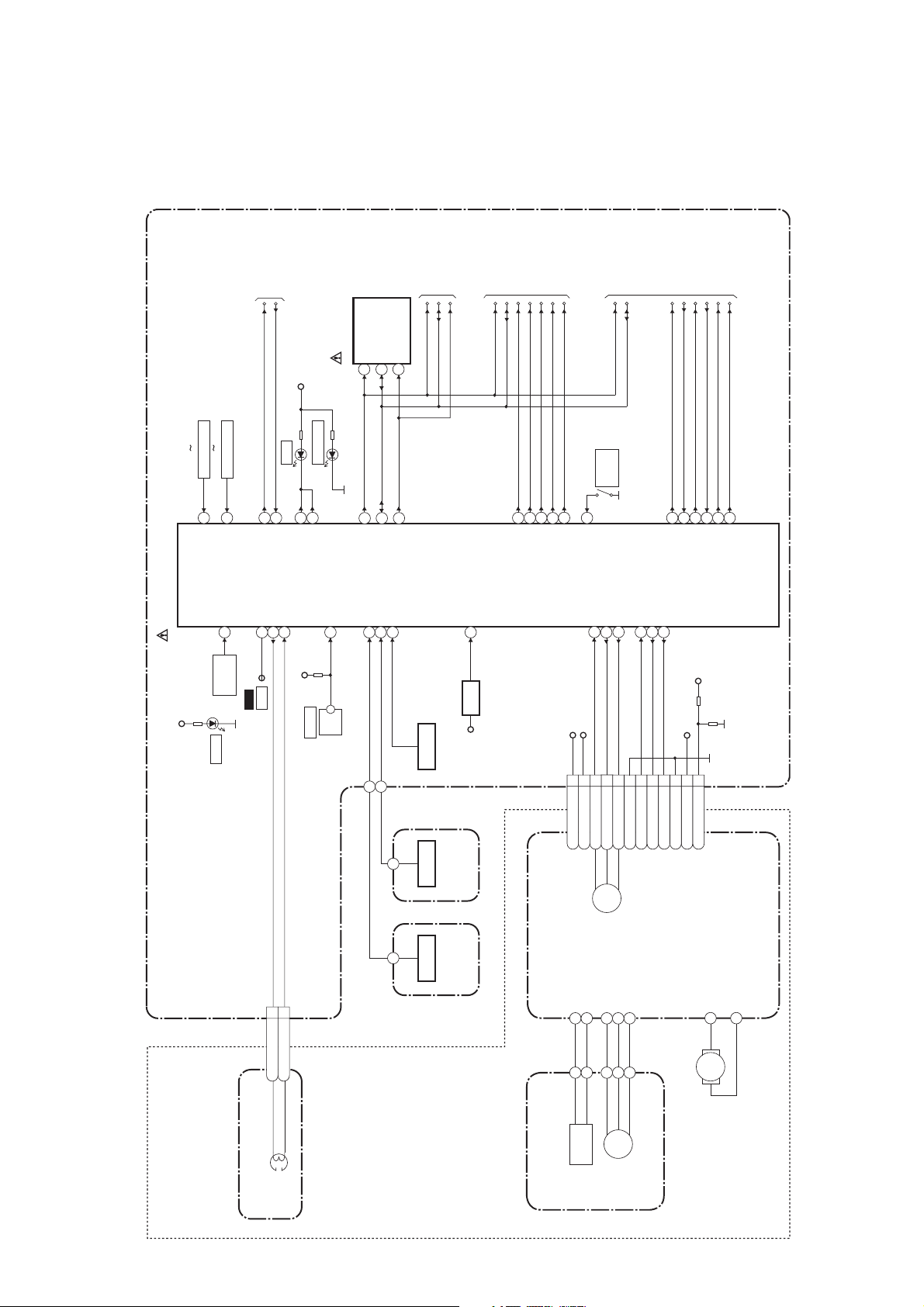
BLOCK DIAGRAMS
Servo/System Control Block Diagram
TO POWER
SUPPLY BLOCK
TO
TV BLOCK
TO
AUDIO BLOCK
TO
VIDEO BLOCK
KEY SWITCH
KEY SWITCH
SW206 SW210
SW201 SW205
8
7
KEY-2
KEY-1
RS201
D201
REMOTE
14
REMOTE
SENSOR
S-LED
TP001
WF3
IC201
(SERVO/SYSTEM CONTROL)
AL+5V
P-ON-H
P-DOWN-L
D202 REC
85
67
P-ON-H
P-DOWN-L
CTL AMP-OUT
CTL(-)
CTL(+)
94
95
97
CTL
AL+5V
D204 STANDBY
24
23
REC-LED
REC-LED
AL+5V
LD-SW
SW212
LD-SW9
(MEMORY)
SCL
IC202
6
71
SCL
ST-SENS.
10480
SDA
CS7
5
72
45
SDA
C-OPEN
2
I
T-REEL
END-SENS.
SCL
T-REEL
SDA
C-OPEN
2
I
Q204
SCL
RESET
34
RESET
TIMER+5V
SDA
SP-MUTE
A-MUTE-H
20
44
SP-MUTE
A-MUTE-H
EXT-L
SCART-H
424829
EXT-L
SCART-H
SCART-MUTE
SW211
31
REC-SAFETY
SCART-MUTE
C-FG
87
CM+12V
P-ON+5V(3)
1CM+12V
2P-ON+5V(3)
3C-FG
CN201
SCL
REC
SAFETY
C-F/R
78
4C-F/R
SDA
C-CONT
76
6FG-GND
5
D-REC-H
LD-CONT81D-CONT
D-PFG
77
90
7LD-CONT
8D-CONT
9
C-SYNC
DV-SYNC
74
47
C-SYNC
D-REC-H
AL+12V(1)
10M-GND
11AL+12V(1)
V-ENV
C-ROTA
6
15
13
V-ENV
C-ROTA
DV-SYNC
+33V
12VG
RF-SW
18
RF-SW
MAIN CBA
)
ASSEMBLY
(DECK
CL402
2CTL(+)
1CTL(-)
ACE HEAD ASSEMBLY
CONTROL
HEAD
END-SENS.
ST-SENS.
Q202 Q205Q201
SENSOR CBA
(END-SENSOR)
SENSOR CBA
(ST-SENSOR)
1-9-1
C-CONT
M
CAPSTAN
PG
SENSOR
MOTOR
M
DRUM
MOTOR
CAPSTAN MOTOR
CYLINDER ASSEMBLY
D-PFG
M
LOADING
MOTOR
T6609BLS
Page 31
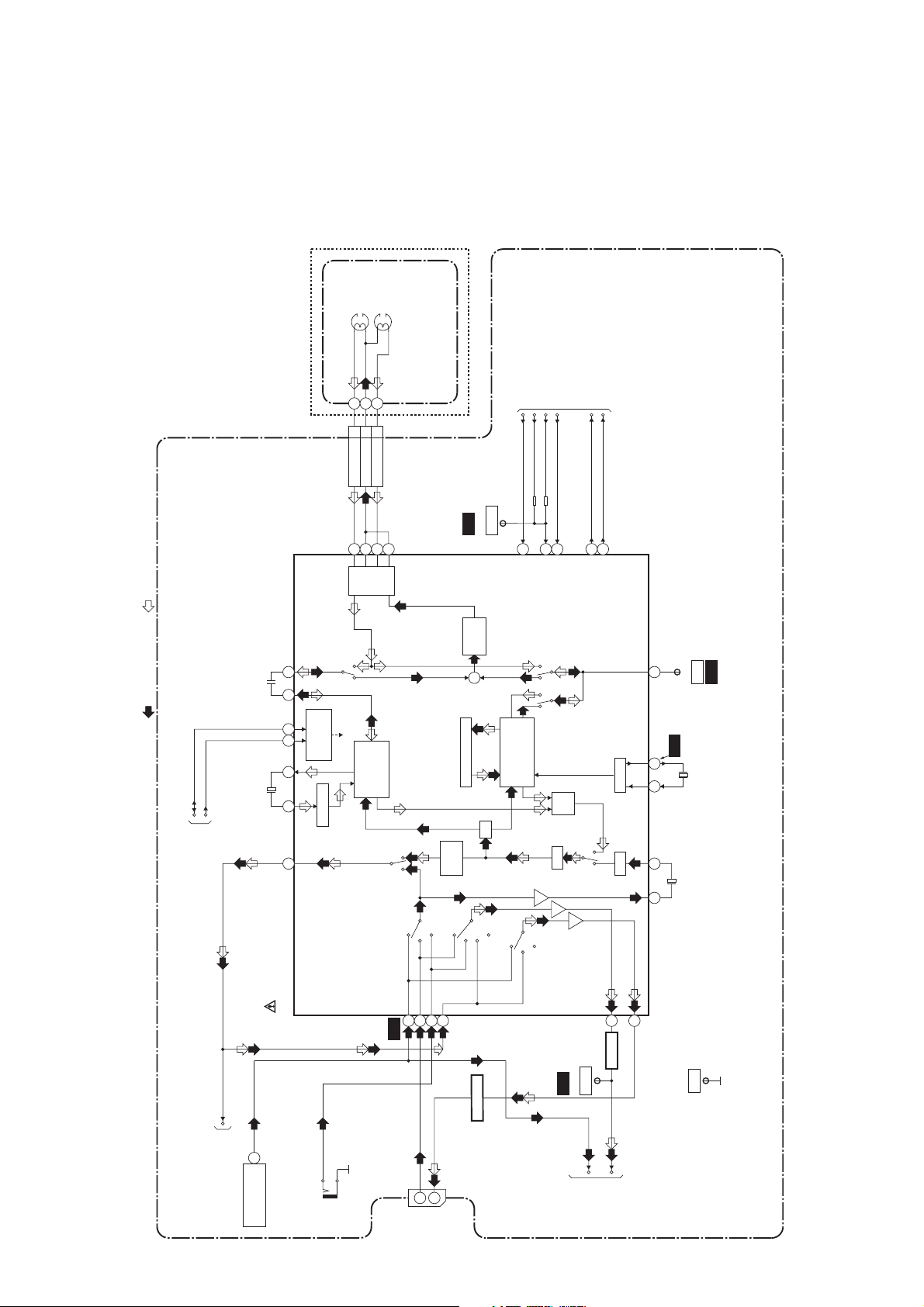
Video Block Diagram
VIDEO (L)
HEAD
VIDEO (R)
HEAD
CYLINDER ASSEMBLY
(DECK ASSEMBLY)
123
V(L)
V(R)
CL401
V-COM
969593
94
WF1
TP002
RF-SW
RF-SW
D-REC-H
80
C-ROTA
TO SERVO/SYSTEM
CONTROL BLOCK
V-ENV
C-SYNC
DV-SYNC
84
62
70
67
SP
HEAD
AMP
SERIAL
DECORDER
Y. DELAY
P
R
LUMINANCE
SIGNAL
PROCESS
7978
REC-VIDEO SIGNAL PB-VIDEO SIGNAL MODE: SP/REC
69684643
SDA
SCL
65
TO
SERVO/SYSTEM
CONTROL BLOCK
IC401
(VIDEO/AUDIO SIGNAL PROCESS)
WF4
AGC
BYPASS
TUNER
SCART
485254
LINE
Y
CCD 1H DELAY
CHARA.
INS.
SCART
LINE
56
REC FM
AGC
+
C
1/2
MUTE
PB/EE
D-REC-H
RF-SW/C-ROTA
RPRP
CHROMINANCE
SIGNAL
PROCESS
MUTE
TUNER
PB/EE
DV-SYNC
Y/C
MIX
FBC
V-ENV
C-SYNC
PR
21
2928
AGC VXO
58 59
61
63
WF2
C-PB
TP008
X401
WF6
4.43MHz
TO
MAIN CBA
C-VIDEO
TV BLOCK
TU001
17
VIDEO OUT
JK701
V-IN
JK703
20
V-IN
19
V-OUT
1-9-2
BUFFER
Q703
WF5
V-OUT
TP003
TU-VIDEO
TO
BUFFER
Q401
VIDEO
TV BLOCK
GND
TP010
T6609BLV
Page 32
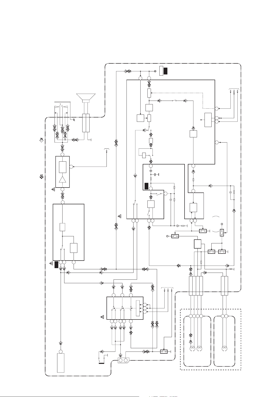
Audio Block Diagram
SP151
SPEAKER
JK151
Mode : SP/REC
PB-AUDIO SIGNAL REC-AUDIO SIGNAL
HEADPHONE JACK
1
AMP
MUTE
OUTPUT
CL801
CN804
SP2SP-GND 1
5
TO
SERVO/SYSTEM
CONTROL BLOCK
SP-MUTE
ALC
12
DET
INV
LINE
R
11
MUTE
AMP
ALC
ATT
98
WF8
N-A-PB
TP007
TO
SERVO/SYSTEM
CONTROL BLOCK
SCL
SDA
A-MUTE-H
SERIAL
DECODER
AUDIO HD-SW
CONTROL
71
68 69
16
REC-ON
P
REC
AMP
100
IC151 (AMP)
7
MAIN CBA
50
ATT
(VIDEO/AUDIO/CHROMA/DEFLECTION/IF)
LINE
TUNER
IC301
52
53
WF7
AUDIO
54
MUTE
IC701 (SW)
WF9
7
EQ
AMP
SP/LP-ON
PB-ON
TUNER
LINE
IC401
(AUDIO SIGNAL PROCESS)
13
4
14
SCART
LINE
SCART
LINE
1
2155
3
12
17
SW CTL
5
6
+5V
Q854
TO SERVO
/SYSTEM
CONTROL
BLOCK
EXT-L
SCART-H
1011 9
SCART-MUTE
CL402
3 A-PB/REC
3
AUTO
1
Q855
BIAS
2
BIAS
4 A-COM
6 AE-H/FE-H
OSC
5 FE-H
Q856
Q853(PB=ON)
+5V
SWITCHING
D-REC-OFF
Q851
CL403
1 FE-H
Q852(PB=ON)
2 FE-H-GND
TU001
6
AUDIO OUT
JK702
A-IN
JK703
2
A-IN
1
A-OUT
1-9-3
Q701
AUDIO
HEAD
AUDIO
ERASE
HEAD
(DECK ASSEMBLY)
FE HEAD
ACE HEAD ASSEMBLY
FULL
ERASE
HEAD
T6609BLA
Page 33
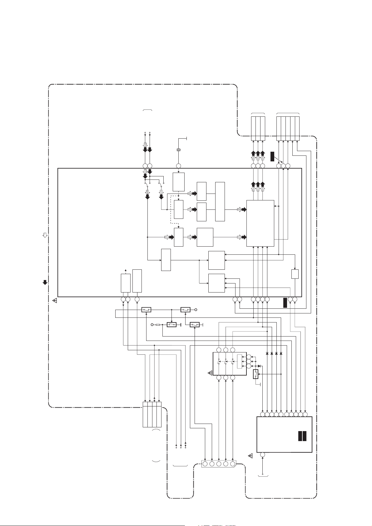
TV Block Diagram
TO
VIDEO BLOCK
TU-VIDEO
VIDEO
36
34
X301
4.43MHz
TO
CRT/H.V. BLOCK
CL302A
WF11
CL302B
V-DRIVE3
FBP2
H-DRIVE1
ACL5
V-RAMP-FB4
6
7
TO
CRT/H.V. BLOCK
CL301B
BLUE2
GREEN1
RED
3
CL301A
32
143115
16
Mode : SP/REC
REC VIDEO SIGNAL PB VIDEO SIGNAL
IC301 (VIDEO/AUDIO/CHROMA/DEFLECTION/IF)
MAIN CBA
SERIAL
I/F
11
10
LINE/PB
INTELLIGENT
MONITORING
43
Q711
+5V
TUNER
LINE/PB
TUNER
SYNC
SEPARATION
Q706
CLOCK
CONTROL
CHROMA
BPF
CHROMA
TRAP
CIRCUIT
Q704
Q702
SECAM
DECODER
PAL
DECODER
LUMA
SIGNAL
+5V
PROCESS
CIRCUIT
H-SYNC
V-SYNC
IC703 (SW)
BASE BAND
1H DELAY LINE
PROCESS
CIRCUIT
PROCESS
CIRCUIT
341
OSD MIX/RBG MATRIX/
BLANKING
INV
21
17
15
SW CTL
13 14
109 11
27
Q710
30
28
20
WF10
12
13
1
CN303
C-OPEN 2
2
INT.MONITOR
I
SDA 4
SCL 5
(NO CONNECTION)
CN303 is used for
adjustment at factory
SCL
C-OPEN
2
I
TO
SERVO/SYSTEM
1-9-4
SDA
CONTROL BLOCK
JK703
SLOW-SW
7
16811
OSD-B
RAPID-SW
OSD-G
15
OSD-R
IC201
(SYSTEM CONTROL/OSD)
64
82
OSD-R
TEXT-L
C-VIDEO
56
C-VIDEO
TO
VIDEO
BLOCK
OSD-B
OSD-G
606263
OSD-BLK
SLOW-SW-IN
616568
59
V-SYNC
RGB CONT
RAPID-SW-IN
WF18
58
H-SYNC
WF17
T6609BLT
Page 34
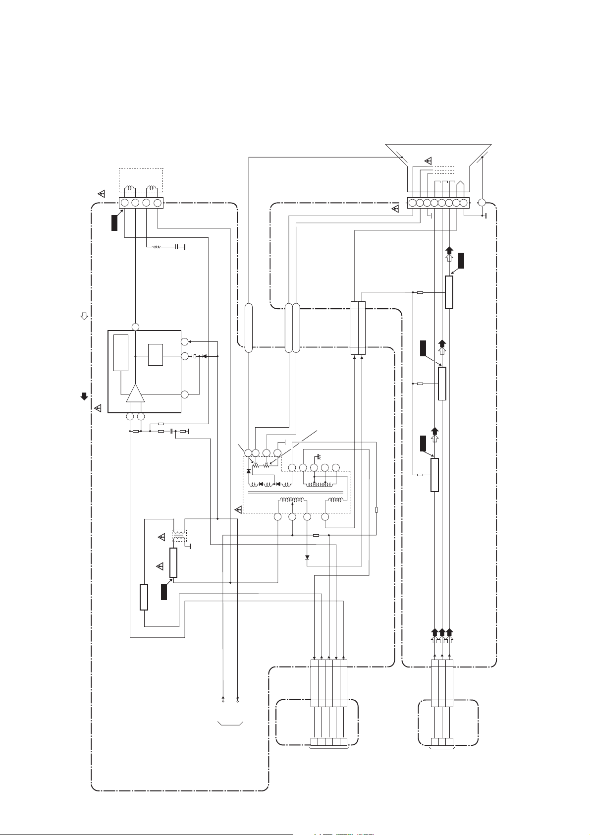
CRT/H.V. Block Diagram
V-
DRIVEH-DRIVE
L551
DEFLECTION-YOKE
543
WF13
Mode : SP/REC
1
CN551
ANODE
JK501
FOCUS
SCREEN
GND
V501
RGB
CRT
HEATER
GND
CN501
WF16
REC VIDEO SIGNAL PB VIDEO SIGNAL
IC551 (V-DEFLECTION CONTROL)
THERMAL
PROTECTION
7
5
AMP
WF15WF14
Q501
Q502
RED AMP
BLUE AMP
Q503
GREEN AMP
CRT CBA
CL501BCL501A
2
VCC
UP
T552
Q551
H.OUTPUT
3
6
PUMP
1
ANODE
FOCUS VR
HV
T551 F.B.T.
F
FOCUS
SCREEN
SCREEN VR
S
11
8107
1
5
3
HEATER 11
P-ON+160V 33
9
6
4
WF12
Q533
H.DRIVE
CN552
33V-DRIVE
11H-DRIVE
22FBP
55ACL
44V-RAMP-FB
H.V./POWER SUPPLY CBA
+B
DEF+B
TO
POWER SUPPLY
BLOCK
CN302CL302B
JUNCTION-B
CBA
125
TO TV
4
BLOCK
CL302A
3
1-9-5
CN502
32RED
CN301CL301B
321
TO TV
14GREEN
23BLUE
BLOCK
CL301A
JUNCTION-C
CBA
T6609BLCRT
Page 35
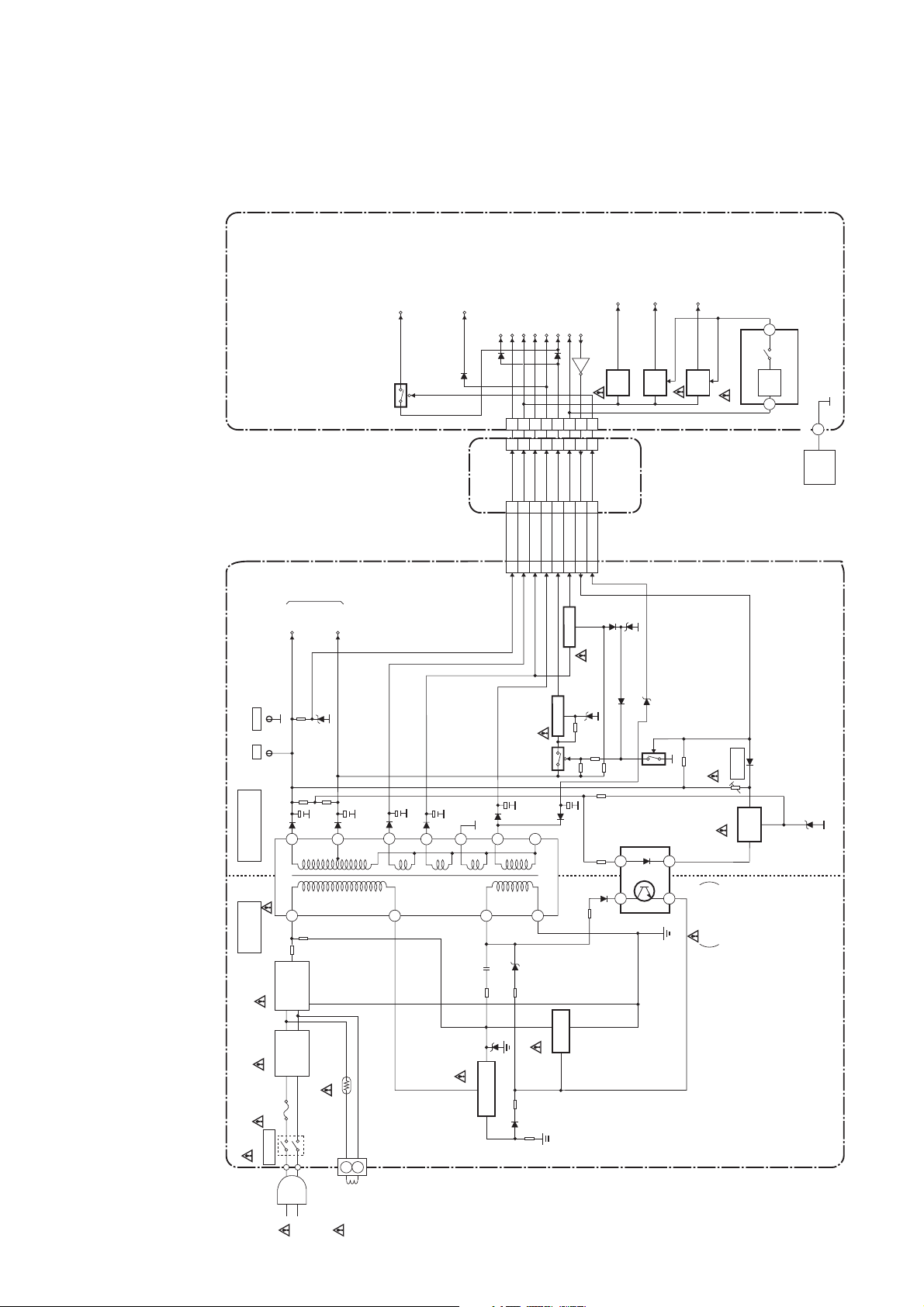
Power Supply Block Diagram
NOTE:
The voltage for parts in hot circuit is measured using
hot GND as a common terminal.
P-DOWN-L
(TO PIN85 OF IC201)
Q206
CM+12V
AL+33V
AL+9V
TIMER+5V
8
CL603A
11
8
11
CL603BCN603
8
11
AL+12V(1)
AL+12V(2)
AL+5V
7
546
3
7
546
3
7
546
3
P-ON+8V
P-ON-H
(TO PIN67 OF IC201)
IC681
Q682
12
12
12
P-ON+5V(3)
P-ON+5V(2)
+5V
REG.
+5V
Q684
JUNCTION-A
CBA
REG.
P-ON+5V(1)
Q686
+5V
REG.
IC301
3955
P-ON-ON
+5.7V
REG.
CL604
TOP
MAIN CBA
COVER
TO
CRT/H.V.
+B
GND
TP504
+B
CAUTION !
For continued protection against fire hazard,
replace only with the same type fuse.
TP503
14
T601
6
HOT COLD
BRIDGE
RECTIFIER
D601 - D604
BLOCK
DEF+B
13
AL+9V
AL+33V
AL+12V(2)
AL+5V
P-ON+8V
P-ON-L
P-DOWN-L
AL+12V(1)3
7
8
546
11
CN602
12
11
4
9
10
2
8
1
Q606
+5V REG.
Q605
12
+8V REG.
Q607
+B ADJ.
IC601
ERROR
VR601
VOLTAGE DET
Q604
FEED
H.V./POWER SUPPLY CBA
BACK
Q608
4 1
3 2
CAUTION !
Fixed voltage (or Auto voltage selectable) power supply circuit is used in this unit.
If Main Fuse (F601) is blown , check to see that all components in the power supply
circuit are not defective before you connect the AC plug to the AC power supply.
Otherwise it may cause some components in the power supply circuit to fail.
F601 L601
POWER
SW601
LINE
FILTER
T4.0A H 250V
W601
PS602
CN601
DG601
DEGAUSSING
COIL
1-9-6
Q602
SWITCHING
Q603
LIMITER
T6609BLP
Page 36

SCHEMATIC DIAGRAMS / CBA’S AND TEST POINTS
Standard Notes
WARNING
Many electrical and mechanical parts in this chassis
have special characteristics. These characteristics
often pass unnoticed and the protection afforded by
them cannot necessarily be obtained by using
replacement components rated for higher voltage,
wattage, etc. Replacement parts that have these
special safety characteristics are identified in this
manual and its supplements; electrical components
having such features are identified by the mark “!” in
the schematic diagram and the parts list. Before
replacing any of these components, read the parts list
in this manual carefully. The use of substitute
replacement parts that do not have the same safety
characteristics as specified in the parts list may create
shock, fire, or other hazards.
Notes:
1. Do not use the part number shown on these
drawings for ordering. The correct part number is
shown in the parts list, and may be slightly
different or amended since these drawings were
prepared.
2. All resistance values are indicated in ohms
(K = 10
3. Resistor wattages are 1/4W or 1/6W unless
otherwise specified.
4. All capacitance values are indicated in µF
(P = 10
5. All voltages are DC voltages unless otherwise
specified.
3
, M = 106).
-6
µF).
1-10-1 Z13P_SC
Page 37
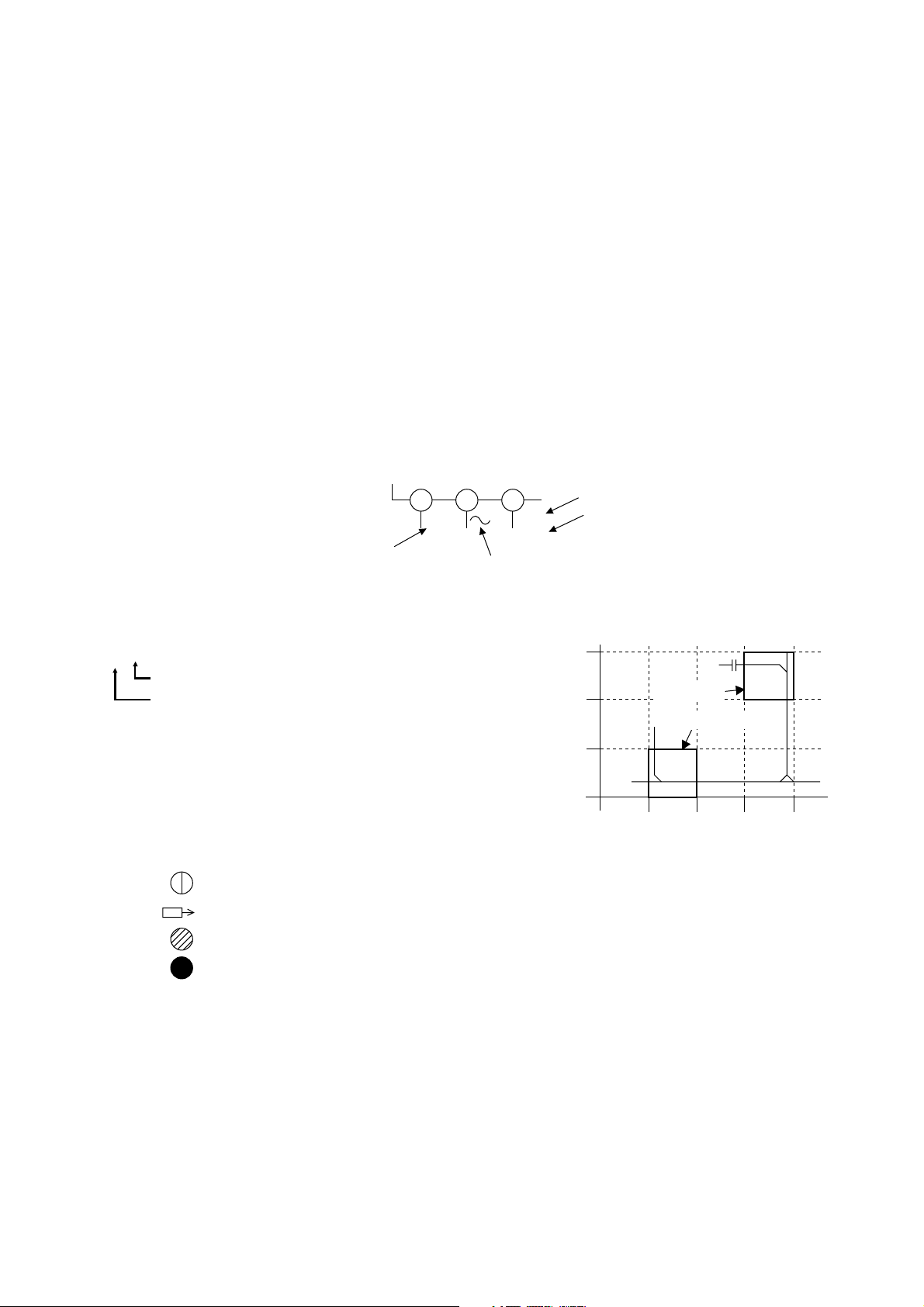
LIST OF CAUTION, NOTES, AND SYMBOLS USED IN THE SCHEMATIC DIAGRAMS ON
THE FOLLOWING PAGES:
1. CAUTION:
FOR CONTINUED PROTECTION AGAINST FIRE HAZARD, REPLACE ONLY WITH THE SAME TYPE
FUSE.
2. CAUTION:
Fixed Voltage (or Auto voltage selectable) power supply circuit is used in this unit.
If Main Fuse (F601) is blown, first check to see that all components in the power supply circuit are not
defective before you connect the AC plug to the AC power supply. Otherwise it may cause some components
in the power supply circuit to fail.
3. Note:
1. Do not use the part number shown on the drawings for ordering. The correct part number is shown in the
parts list, and may be slightly different or amended since the drawings were prepared.
2. To maintain original function and reliability of repaired units, use only original replacement parts which are
listed with their part numbers in the parts list section of the service manual.
4. Mode: SP/REC
5. Voltage indications for PLAY and REC modes on the schematics are as shown below:
Unit: Volts
The same voltage for
both PLAY & REC modes
6. How to read converged lines
1-D3
Distinction Area
Line Number
(1 to 3 digits)
Examples:
1. "1-D3" means that line number "1" goes to the line number
"1" of the area "D3".
2. "1-B1" means that line number "1" goes to the line number
"1" of the area "B1".
7. Test Point Information
: Indicates a test point with a jumper wire across a hole in the PCB.
: Used to indicate a test point with a component lead on foil side.
: Used to indicate a test point with no test pin.
5.0
231
5.0
(2.5)
Indicates that the voltage
is not consistent here.
PLAY mode
REC mode
3
2
1
AREA D3
1-B1
AREA B1
1-D3
ABCD
: Used to indicate a test point with a test pin.
1-10-2 Z13P_SC
Page 38
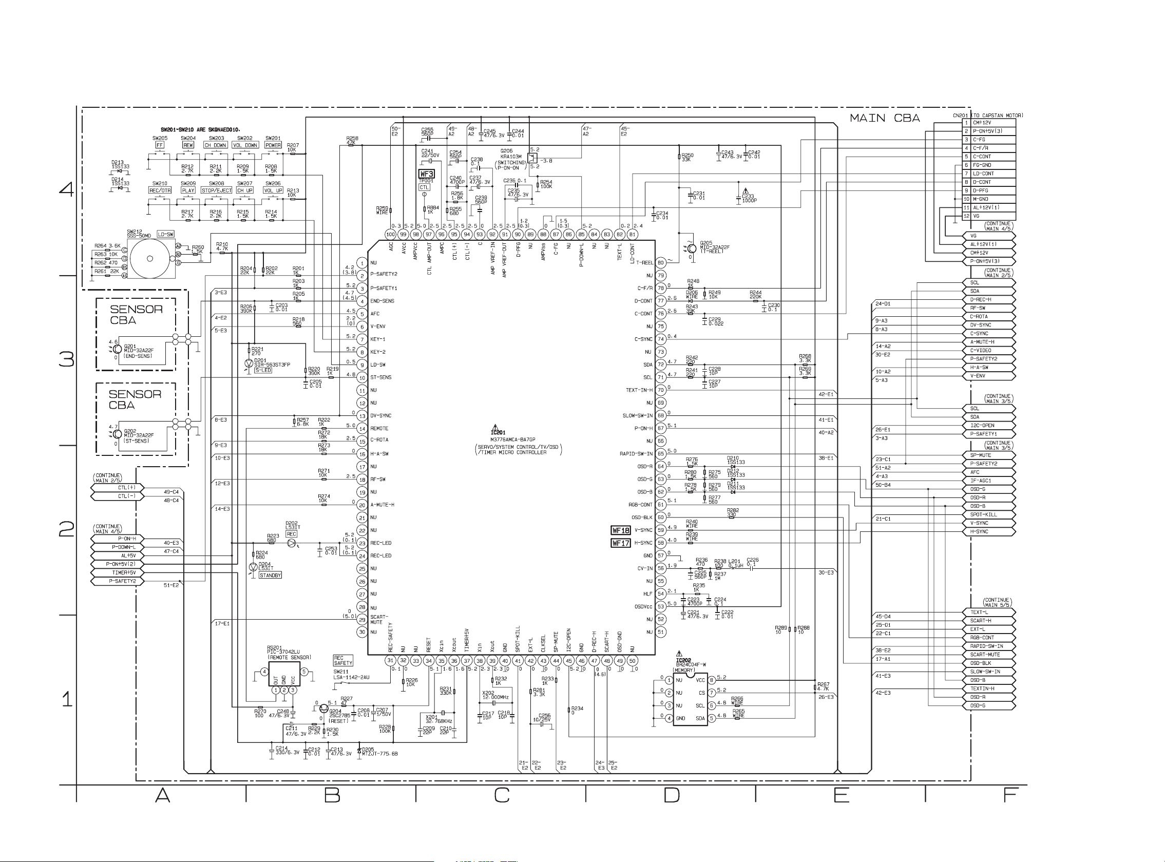
Main 1/5 & Sensor Schematic Diagram
1-10-3
T6609SCM1
Page 39
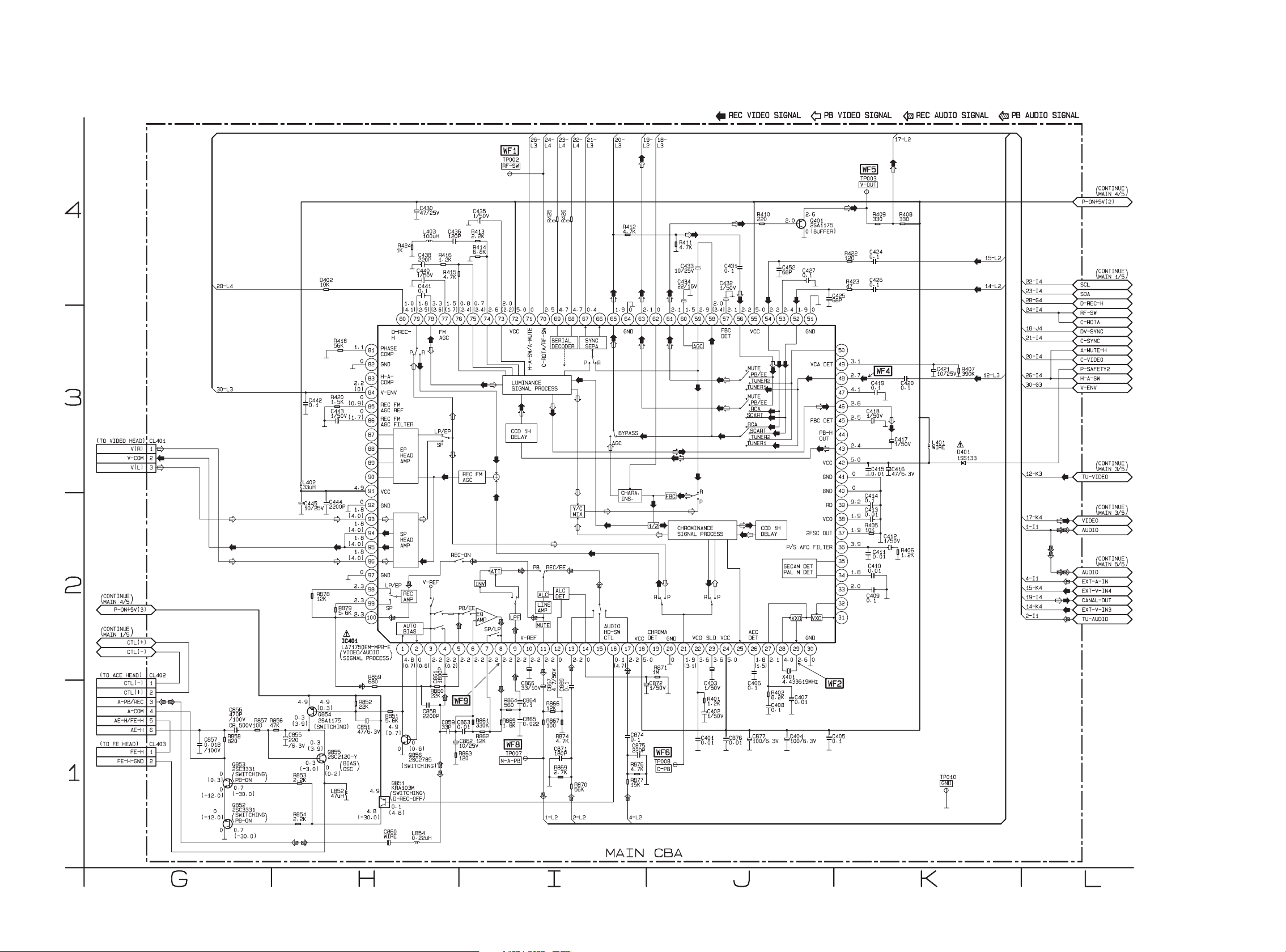
Main 2/5 Schematic Diagram
1-10-4
T6609SCM2
Page 40
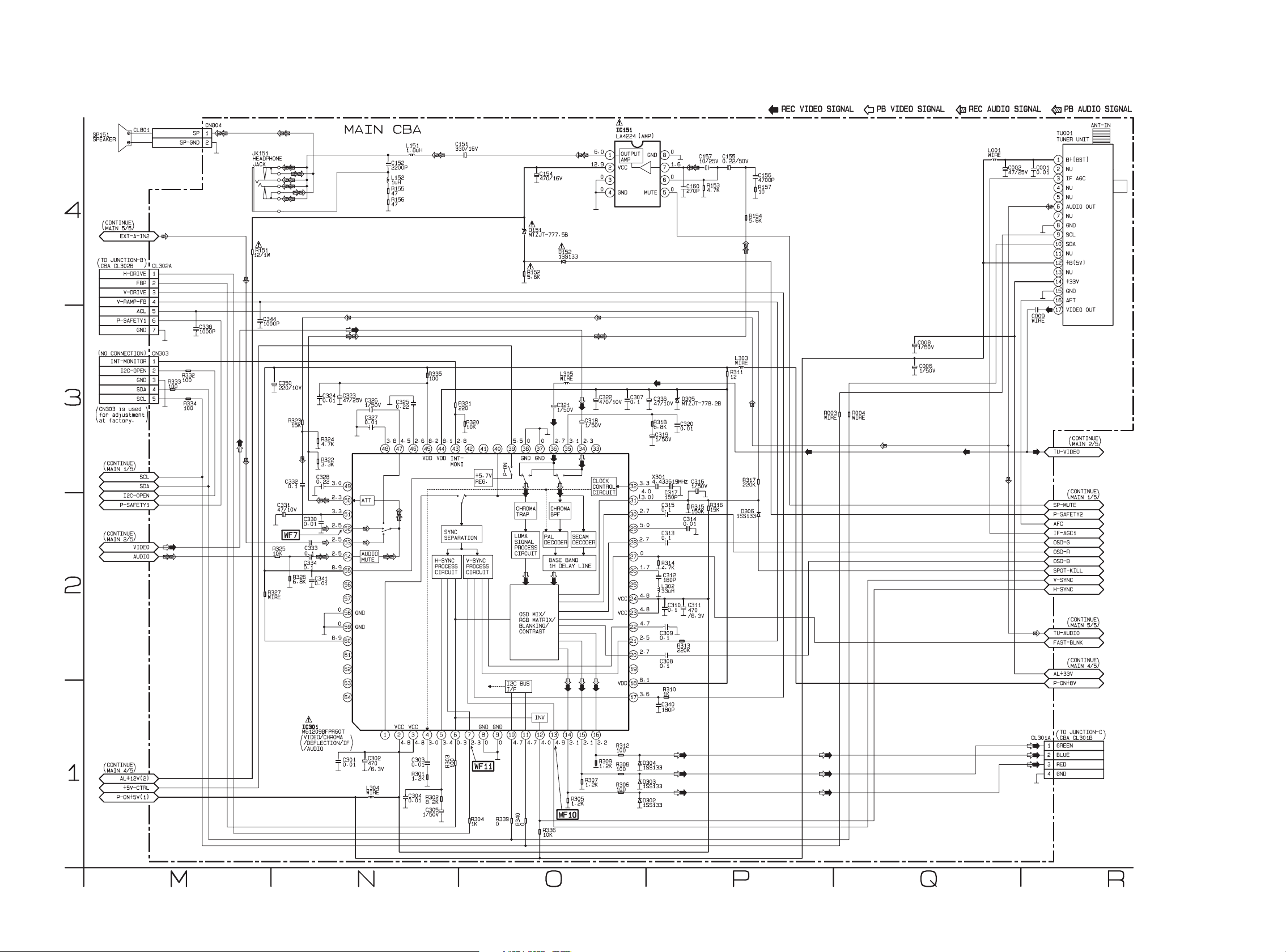
Main 3/5 Schematic Diagram
1-10-5 T6609SCM3
Page 41
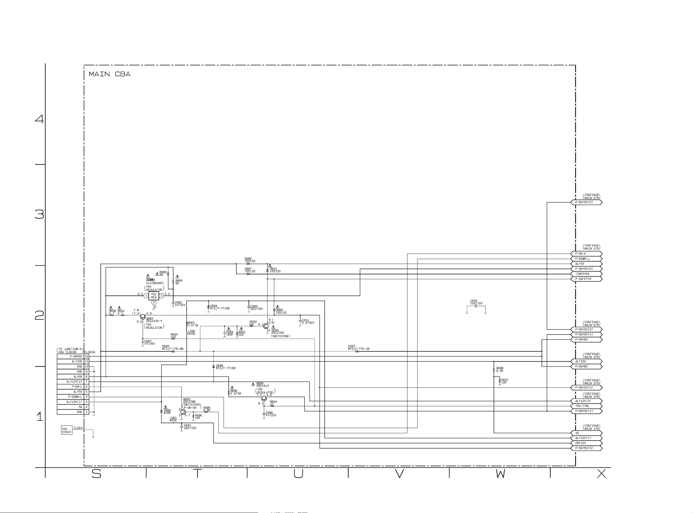
Main 4/5 Schematic Diagram
1-10-6
T6609SCM4
Page 42
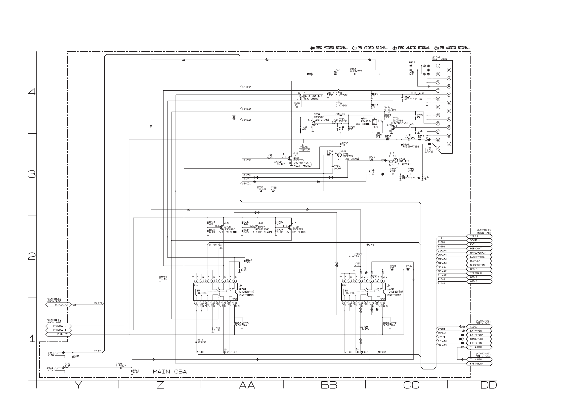
Main 5/5 Schematic Diagram
1-10-7
T6609SCM5
Page 43
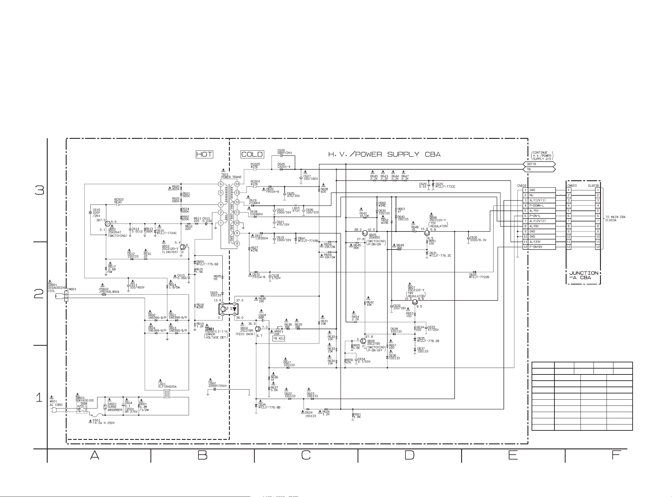
H.V./Power Supply 1/2 & Junction-A Schematic Diagram
Because a hot chassis ground is present in the power
supply circuit, an isolation transformer must be used.
Also, in order to have the ability to increase the input
slowly,when troubleshooting this type power supply
circuit, a variable isolation transformer is required.
NOTE:
The voltage for parts in hot circuit is measured using
hot GND as a common terminal.
Ref. No.
IC601
Ref. No.
Q602
Ref. No.
Q603
Q604
Q605
Q606
Q607
Q608
SDG
1.80304.0
ECB
00.21.8
6.7
10.3
5.9
1.2
12.0
10.3
9.7
9.6
6.5
7.3
1.2
0
5.5
0.1 0. 7
1234
13.1 12.1 0.2 1.6
CAUTION !
Fixed voltage (or Auto voltage selectable) power supply circuit is used in this unit.
If Main Fuse (F601) is blown , check to see that all components in the power supply
circuit are not defective before you connect the AC plug to the AC power supply.
Otherwise it may cause some components in the power supply circuit to fail.
CAUTION !
For continued protection against fire hazard,
replace only with the same type fuse.
VOLTAGE CHART (Power off mode)
1-10-8 T6609SCP1
Page 44
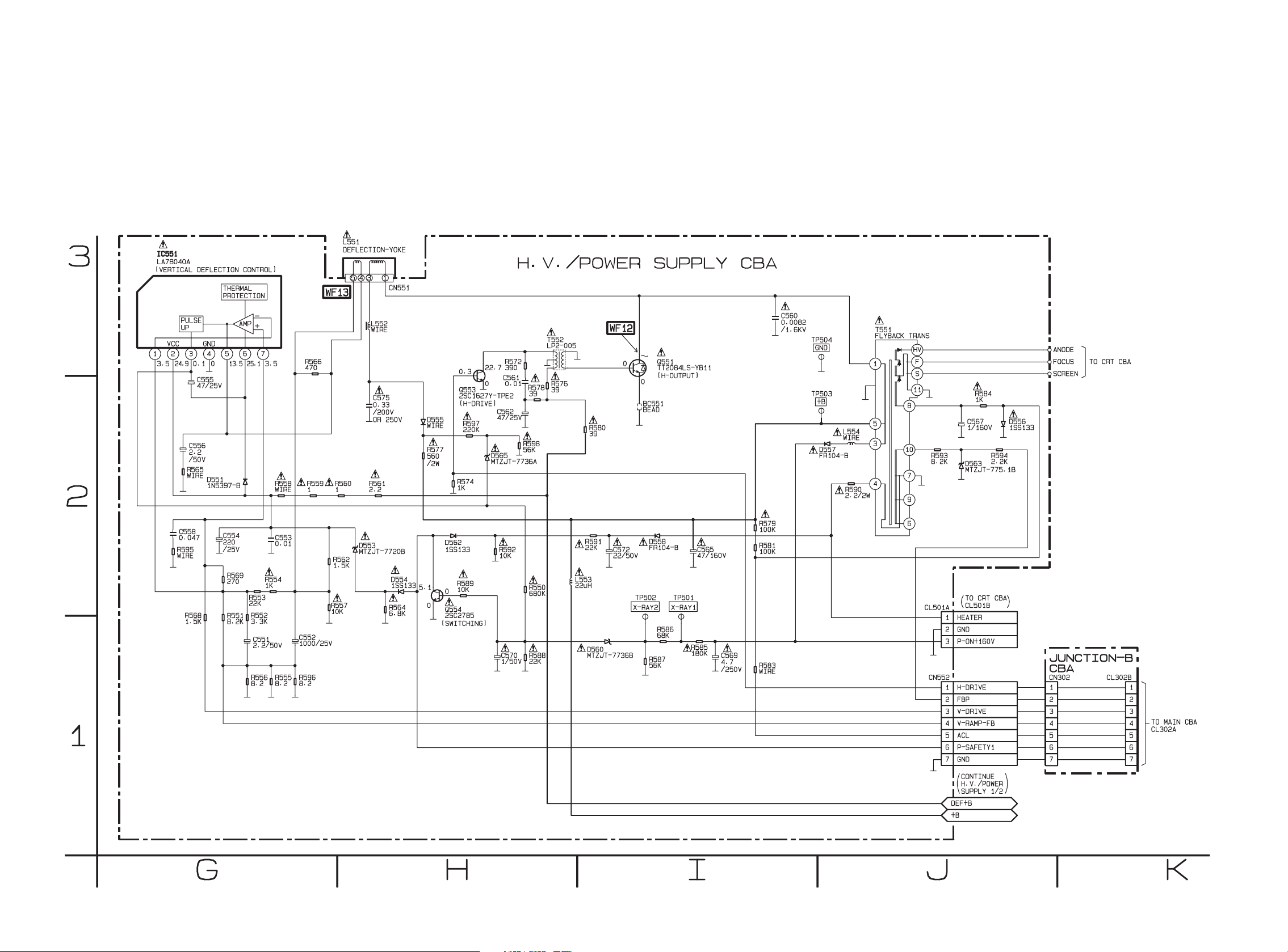
H.V./Power Supply 2/2 & Junction-B Schematic Diagram
1-10-9
T6609SCP2
Page 45
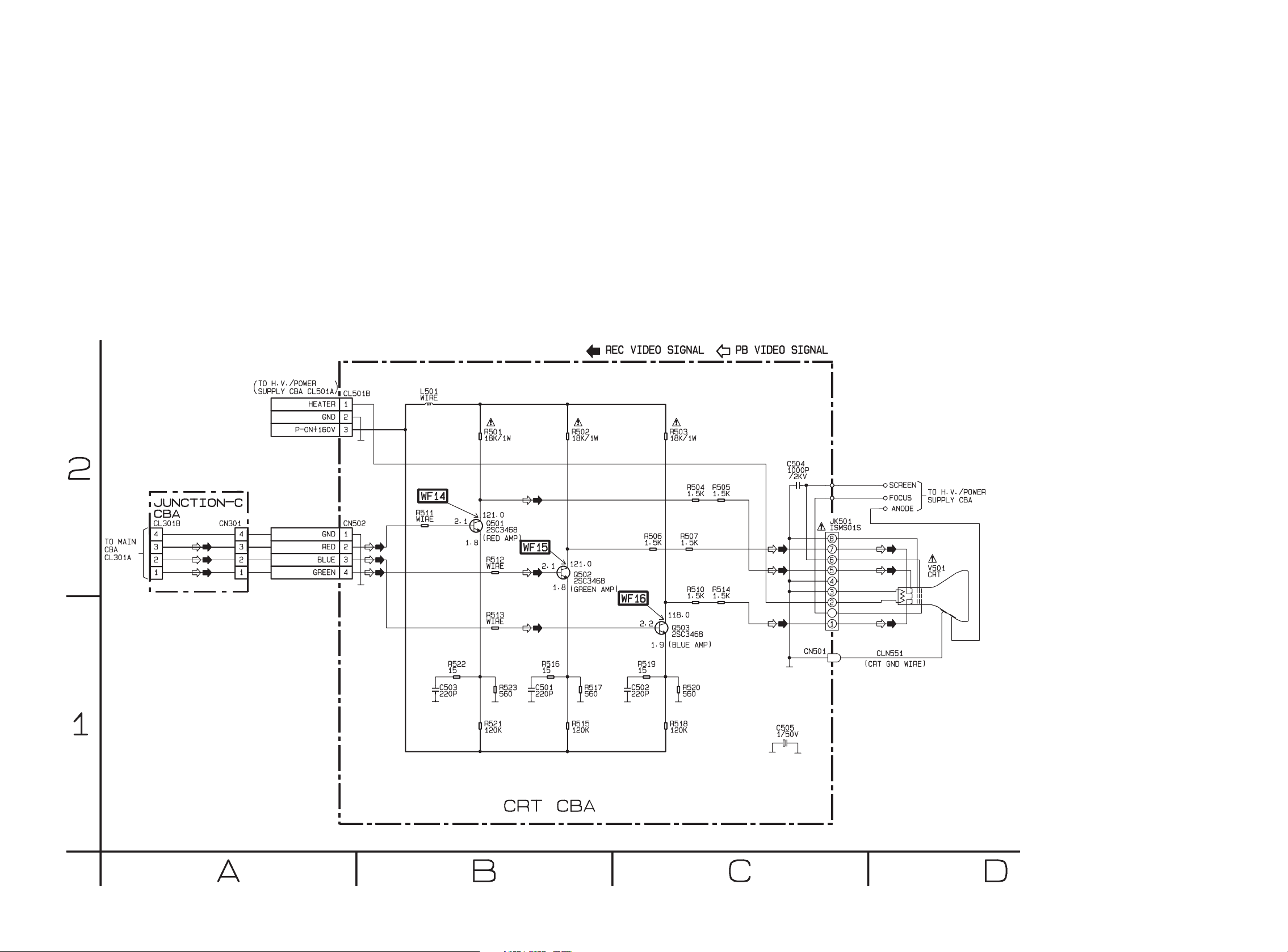
CRT & Junction-C Schematic Diagram
1-10-10
T6609SCCRT
Page 46
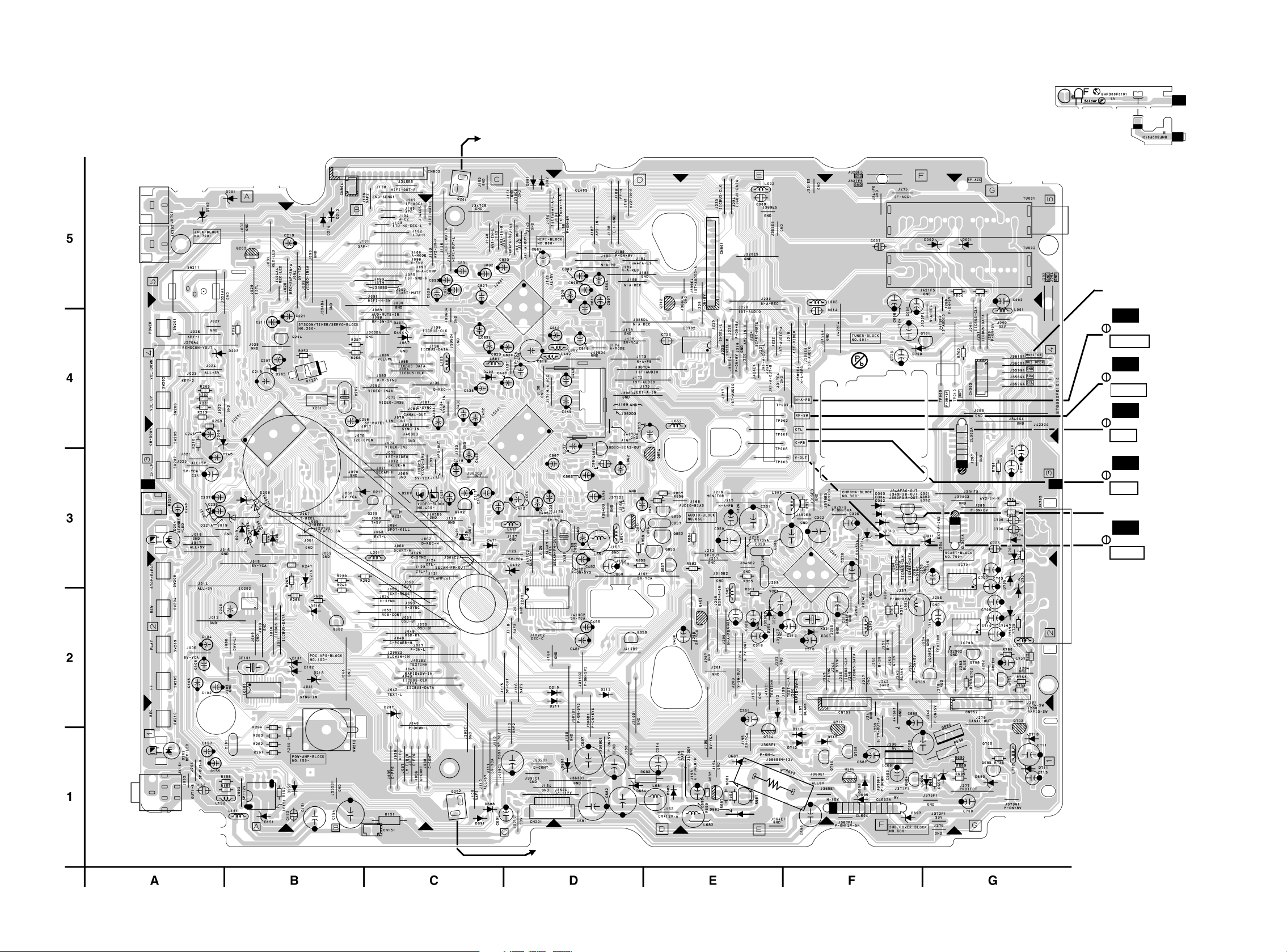
Main CBA Top View
TO SENSOR CBA
(END-SENSOR)
Sensor CBA Top View
BHF300F01011-A
BHF300F01011-B
J361G4
(SECAM Black Level
Adjustment)
WF8
TP007
N-A-PB
WF1
TP002
RF-SW
WF3
TP001
CTL
WF6
TP008
C-PB
J349F3
(C-Trap Adjustment)
WF5
TP003
V-OUT
TO SENSOR CBA
(START-SENSOR)
1-10-11
BT6600F01014
Page 47
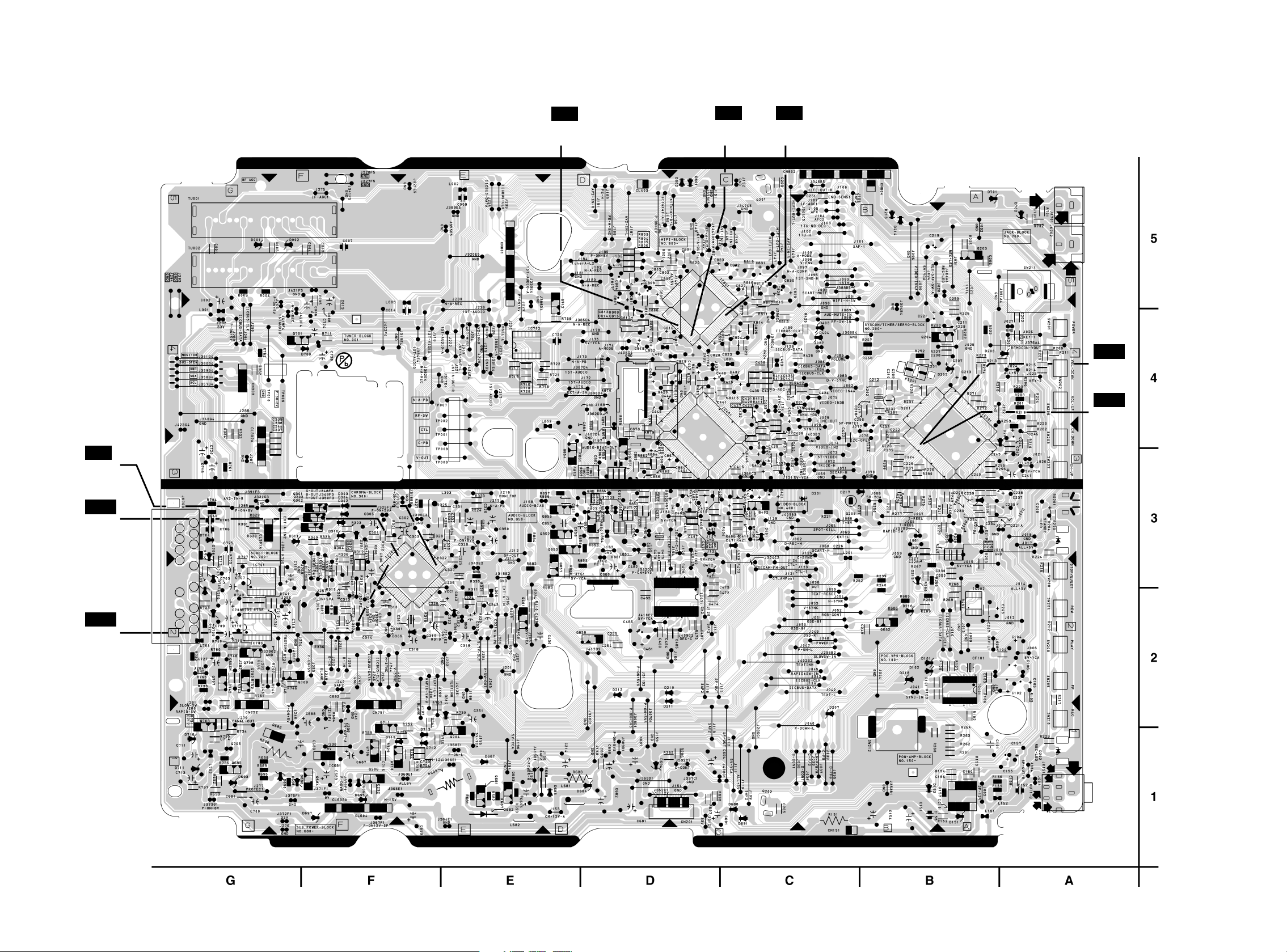
Main CBA Bottom View
WF9
PIN 8
OF IC401
WF2
PIN 29
OF IC401
WF4
PIN 48
OF IC401
WF17
PIN 58
OF IC201
WF18
PIN 59
OF IC201
WF7
PIN 52
OF IC301
WF11
PIN 7
OF IC301
WF10
PIN 13
OF IC301
1-10-12
BT6600F01014
Page 48
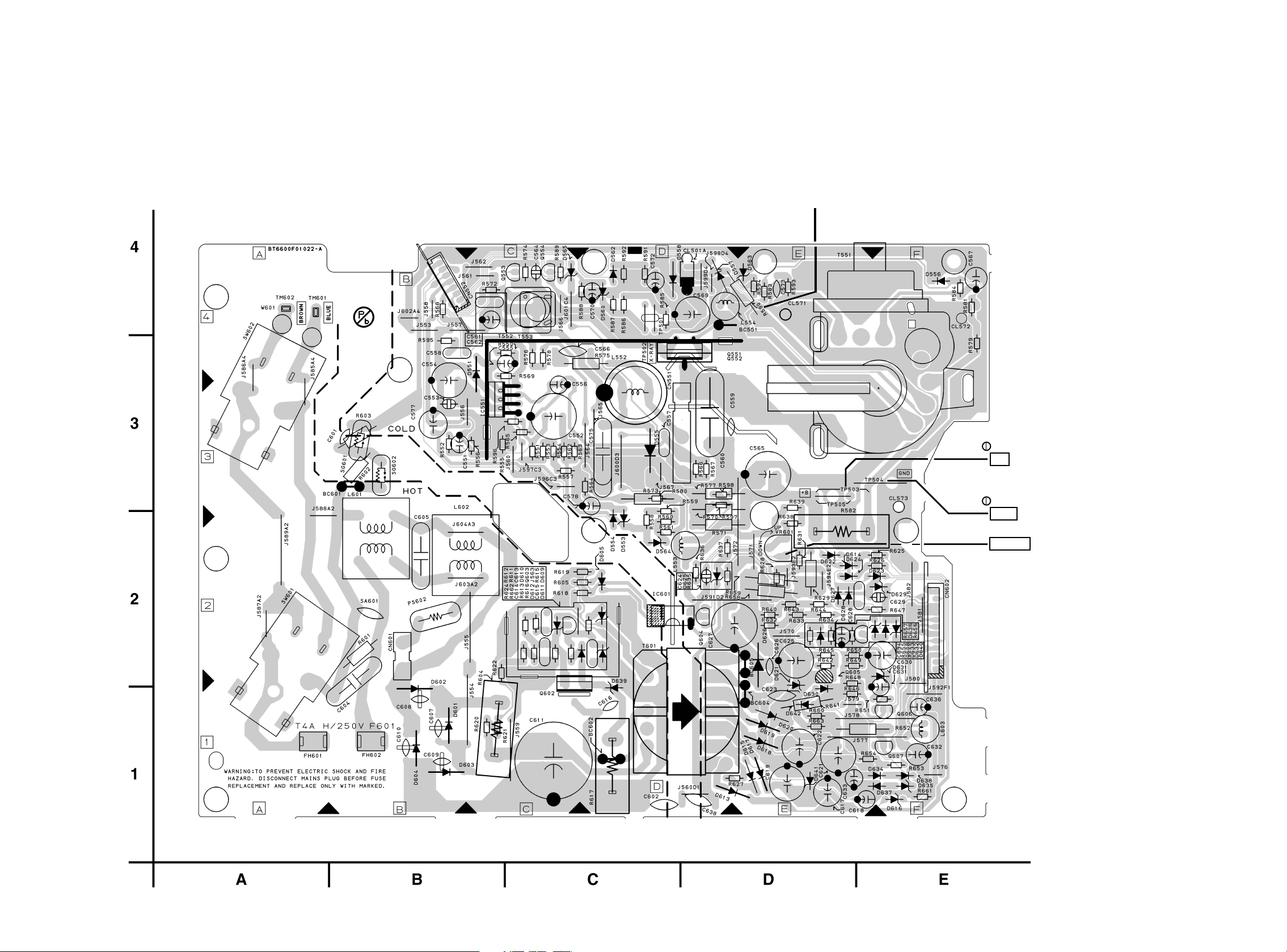
H.V./Power Supply CBA Top View
CAUTION !
Fixed voltage (or Auto voltage selectable) power supply circuit is used in this unit.
If Main Fuse (F601) is blown , check to see that all components in the power supply
circuit are not defective before you connect the AC plug to the AC power supply.
Otherwise it may cause some components in the power supply circuit to fail.
CAUTION !
For continued protection against fire hazard,
replace only with the same type fuse.
NOTE:
The voltage for parts in hot circuit is measured using
hot GND as a common terminal.
Because a hot chassis ground is present in the power
supply circuit, an isolation transformer must be used.
Also, in order to have the ability to increase the input
slowly,when troubleshooting this type power supply
circuit, a variable isolation transformer is required.
R590
(H Adjustment)
TP503
+B
TP504
GND
VR601
+B ADJ
1-10-13
BT6600F01022-A
Page 49
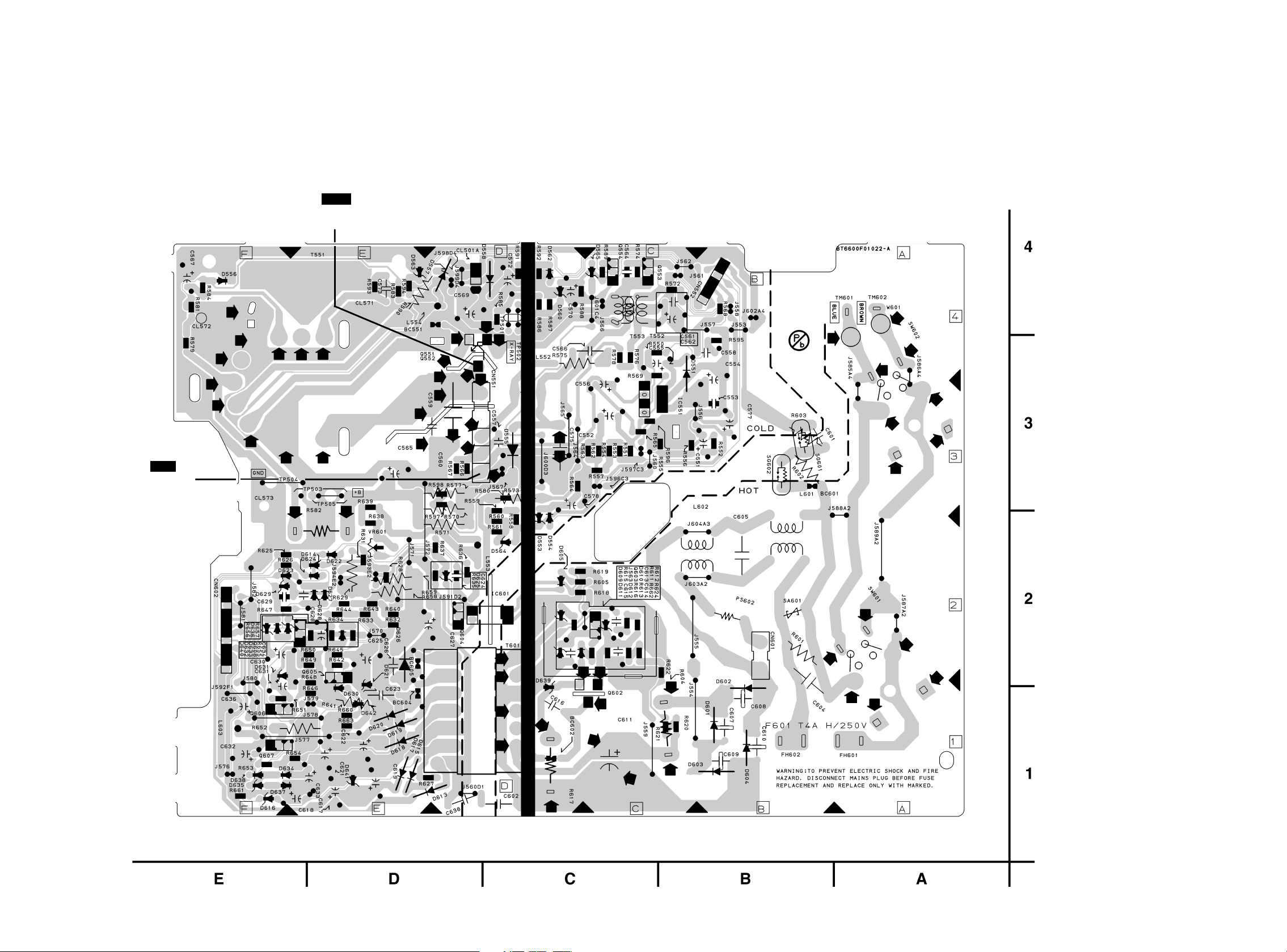
H.V./Power Supply CBA Bottom View
Because a hot chassis ground is present in the power
supply circuit, an isolation transformer must be used.
Also, in order to have the ability to increase the input
slowly,when troubleshooting this type power supply
circuit, a variable isolation transformer is required.
CAUTION !
Fixed voltage (or Auto voltage selectable) power supply circuit is used in this unit.
If Main Fuse (F601) is blown , check to see that all components in the power supply
circuit are not defective before you connect the AC plug to the AC power supply.
Otherwise it may cause some components in the power supply circuit to fail.
WF12
Q551
Collector
CAUTION !
For continued protection against fire hazard,
replace only with the same type fuse.
NOTE:
The voltage for parts in hot circuit is measured using
hot GND as a common terminal.
WF13
PIN 5
OF CN551
1-10-14
BT6600F01022-A
Page 50
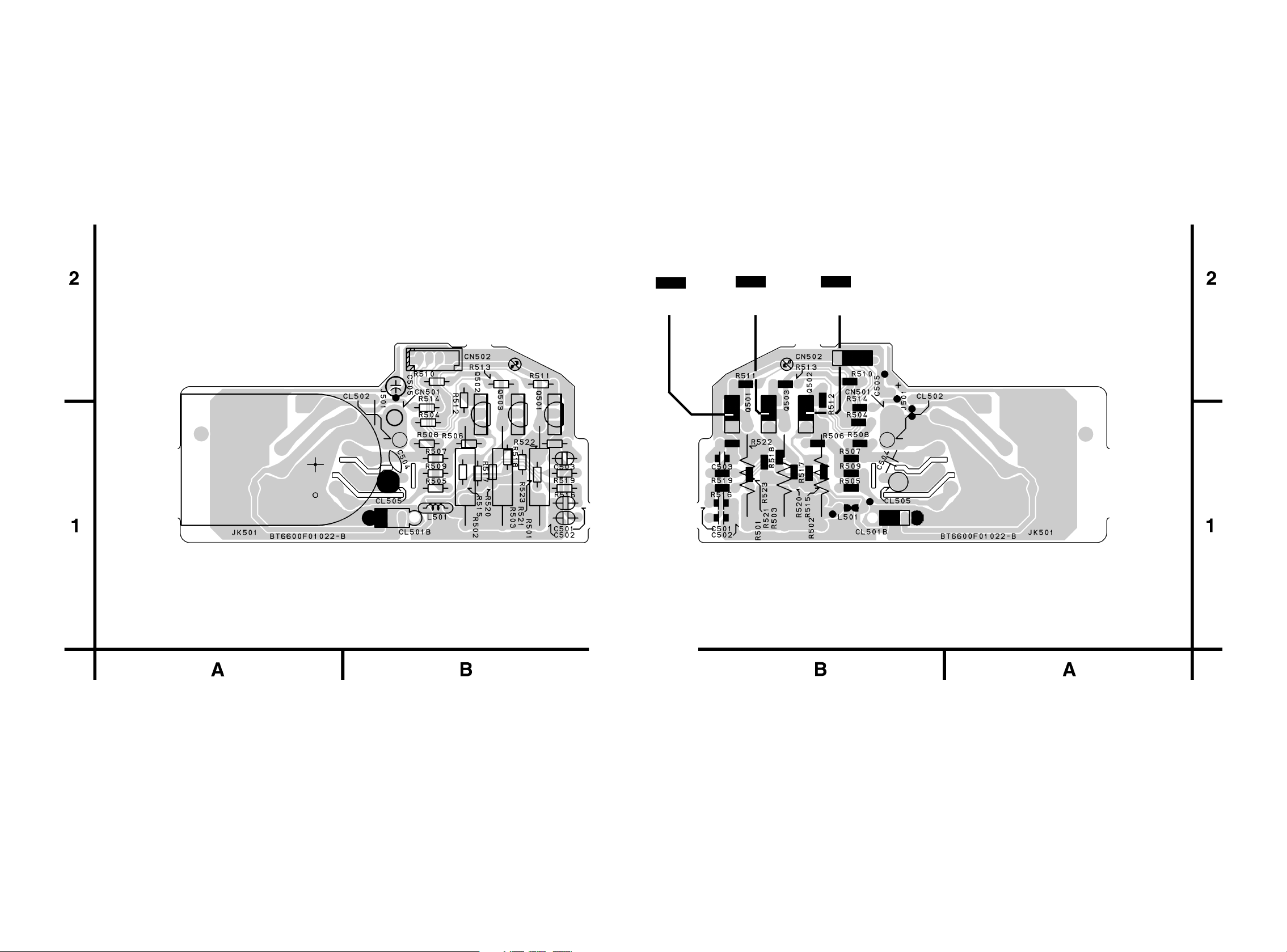
CRT CBA Top View CRT CBA Bottom View
WF14
Q501
Collector
WF16
Q503
Collector
WF15
Q502
Collector
1-10-15
BT6600F01022-B
Page 51
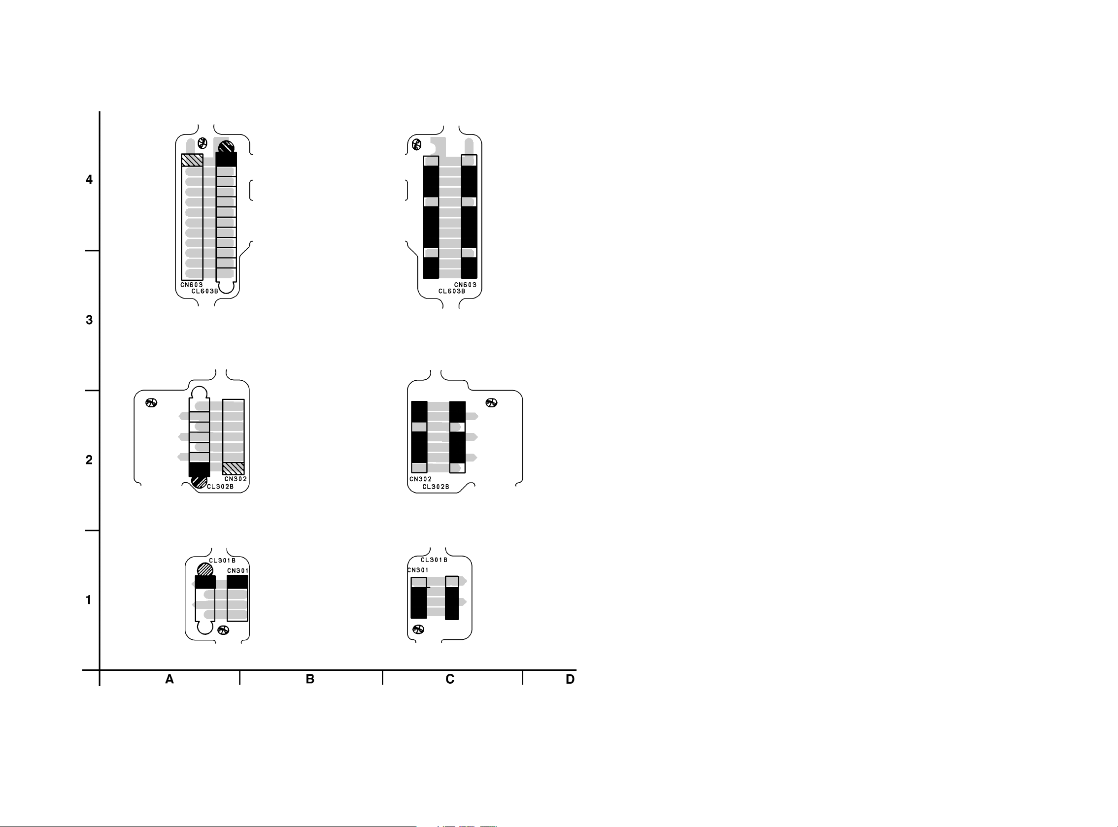
Junction-A CBA Top View
Junction-A CBA Bottom View
Junction-B CBA Top View Junction-B CBA Bottom View
Junction-C CBA Top View Junction-C CBA Bottom View
BT6600F01014
1-10-16
Page 52
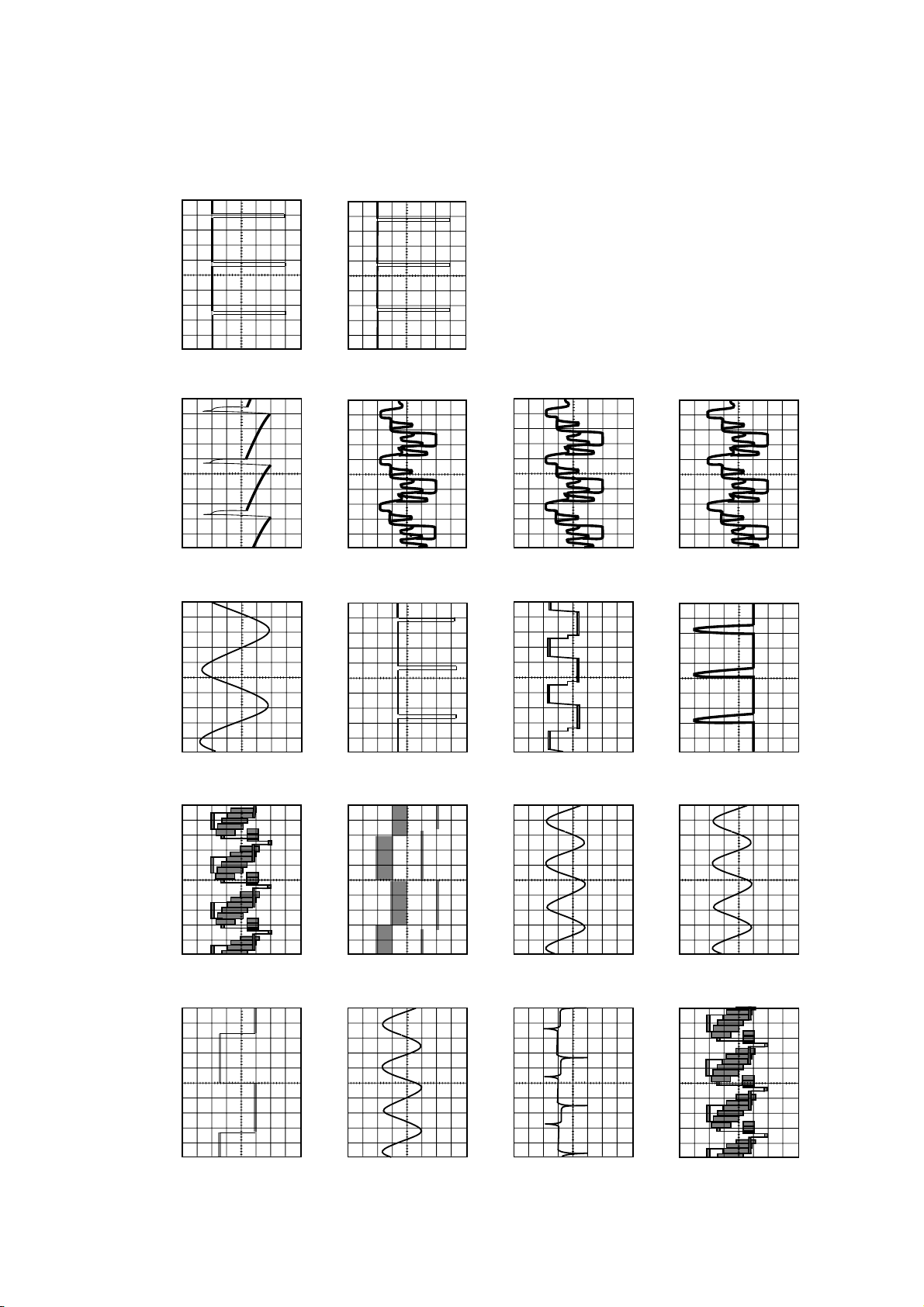
µs
1DIV: 1V 20
IC201 PIN 58
WAVEFORMS
1DIV: 1V 5ms
IC201 PIN 59
WAVEFORM NOTES
INPUT: COLOR BAR SIGNAL
OTHER CONTROLS: CENTER POSITION
VOLTAGES SHOWN ARE RANGE OF
OSCILLOSCOPE SETTING
WF17
1DIV: 10V 5ms
CN551 PIN 5
WF13
1DIV: 0.5V 0.5ms
IC401 PIN 8
WF9
WF18
µs
1DIV: 20V 20
Q501 COLLECTOR
WF14
1DIV: 2V 5ms
IC301 PIN 13
WF10
µs
1DIV: 20V 20
Q502 COLLECTOR
WF15
µs
1DIV: 1V 20
IC301 PIN7
WF11
µs
1DIV: 20V 20
Q503 COLLECTOR
WF16
µs
1DIV: 200V 20
Q551 COLLECTOR
WF12
µs
1DIV: 0.5V 20
TP003 V-OUT
WF5
1DIV: 2V 5ms
TP002 RF-SW
WF1
1DIV: 0.2V 2DIV: 5V 5ms
Upper: WF6 Lower: WF1
µs
1DIV: 0.2V 0.1
IC401 PIN 29
WF2
1-11-1
TP008 C-PB
1DIV: 0.2V 0.5ms
IC301 PIN 52
WF7
1DIV: 1V 10ms
TP001 CTL
WF3
1DIV: 0.5V 0.5ms
TP007 N-A-PB
WF8
µs
1DIV: 0.25V 20
IC401 PIN 48
WF4
Z13PWF
Page 53
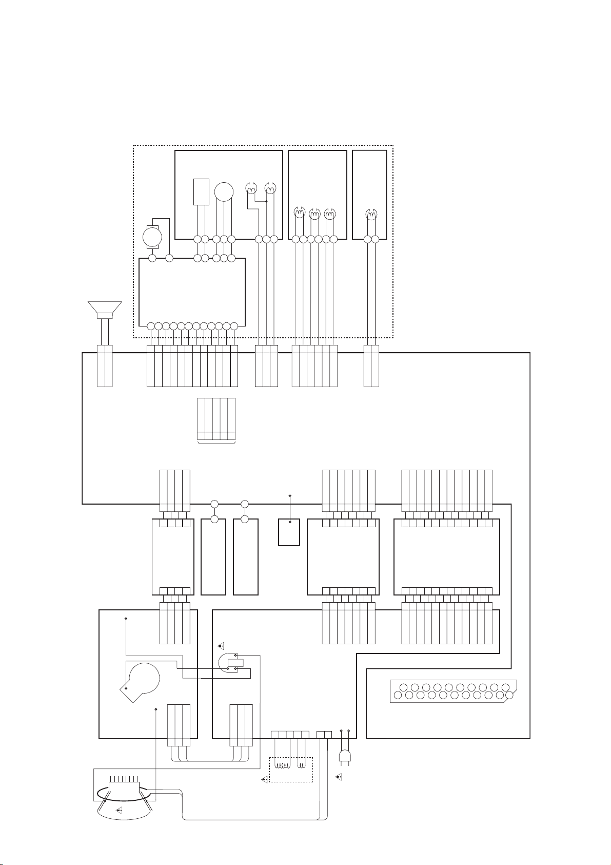
SP151
CL801
2
LOADING
MOTOR
CYLINDER ASSEMBLY
M
SPEAKER
CAPSTAN MOTOR
WIRING DIAGRAM FOR DECK MECHANISM SECTION
1
3
1
2
7
6
4
5
WIRING DIAGRAM
DRUM
MOTOR
VIDEO
(R)
HEAD
VIDEO
(L)
HEAD
M
PG
SENSOR
9
8
3
2
10
11
1
12
CONTROL HEAD
AUDIO HEAD
AUDIO ERASE
HEAD
ACE HEAD ASSEMBLY
FULL ERASE HEAD
FE HEAD
CN804
SP
SP-GND
CN201
SCREEN
P-ON+5V(3)
CM+12V
CL301A
GREEN1
123
CL301B
CN301
123
CN502
GREEN 4
C-FG
BLUE2
BLUE 3
C-F/R
RED3
JUNCTION-C CBA
RED 2
C-CONT
FG-GND
GND4
4
4
GND 1
LD-CONT
CN303
VG
D-PFG
D-CONT
AL+12V(1)
M-GND
C-OPEN2
2
INT.MONITOR1I
GND3
SDA4
SCL5
(NO CONNECTION)
CN303 IS USED FOR
ADJUSTMENT AT
FACTORY
SENSOR CBA
(END-SENSOR)
T551
FBT
CL401
V-COM
V(R)
SENSOR CBA
(ST-SENSOR)
V(L)
CL402
CL604
TOP
COVER
CL403
CTL(-) 1
CTL(+) 2
A-PB/REC 3
A-COM 4
AE-H/FE-H 5
AE-H 6
FE-H 1
FE-H-GND 2
MAIN CBA
CL302A
H-DRIVE1
FBP2
12345
CL302BCN302
12345
CN552
H-DRIVE 1
FBP 2
V-DRIVE3
V-RAMP-FB4
ACL5
P-SAFETY16
6
JUNCTION-B CBA
6
V-DRIVE 3
V-RAMP-FB 4
ACL 5
P-SAFETY1 6
CL603A
GND1
NU2
AL+12V(1)3
P-DOWN-L4
AL+5V5
P-ON-L6
AL+12V(2)7
AL+9V8
GND9
GND10
AL+33V11
P-ON+8V12
77 GND7GND 7
123456789
CL603B
CN603
123456789
CN602
GND 1
NU 2
AL+12V(1) 3
P-DOWN-L 4
AL+5V 5
P-ON-L 6
101112
JUNCTION-A CBA
101112
AL+12V(2) 7
AL+9V 8
GND 9
GND 10
AL+33V 11
P-ON+8V 12
ANODE
FOCUS
123456789
CRT CBA
CN551
D.Y.
H.V. / POWER SUPPLY CBA
1
CN601
2
5
1
3
HD
2
4
VD
W601
CN501
CL501B
HEATER1
GND2P-ON+160V3
GND
CRT
CL501A
HEATER1
GND2P-ON+160V3
JK703
1-12-1
1011121314151617181920
21
T6609WI
Page 54
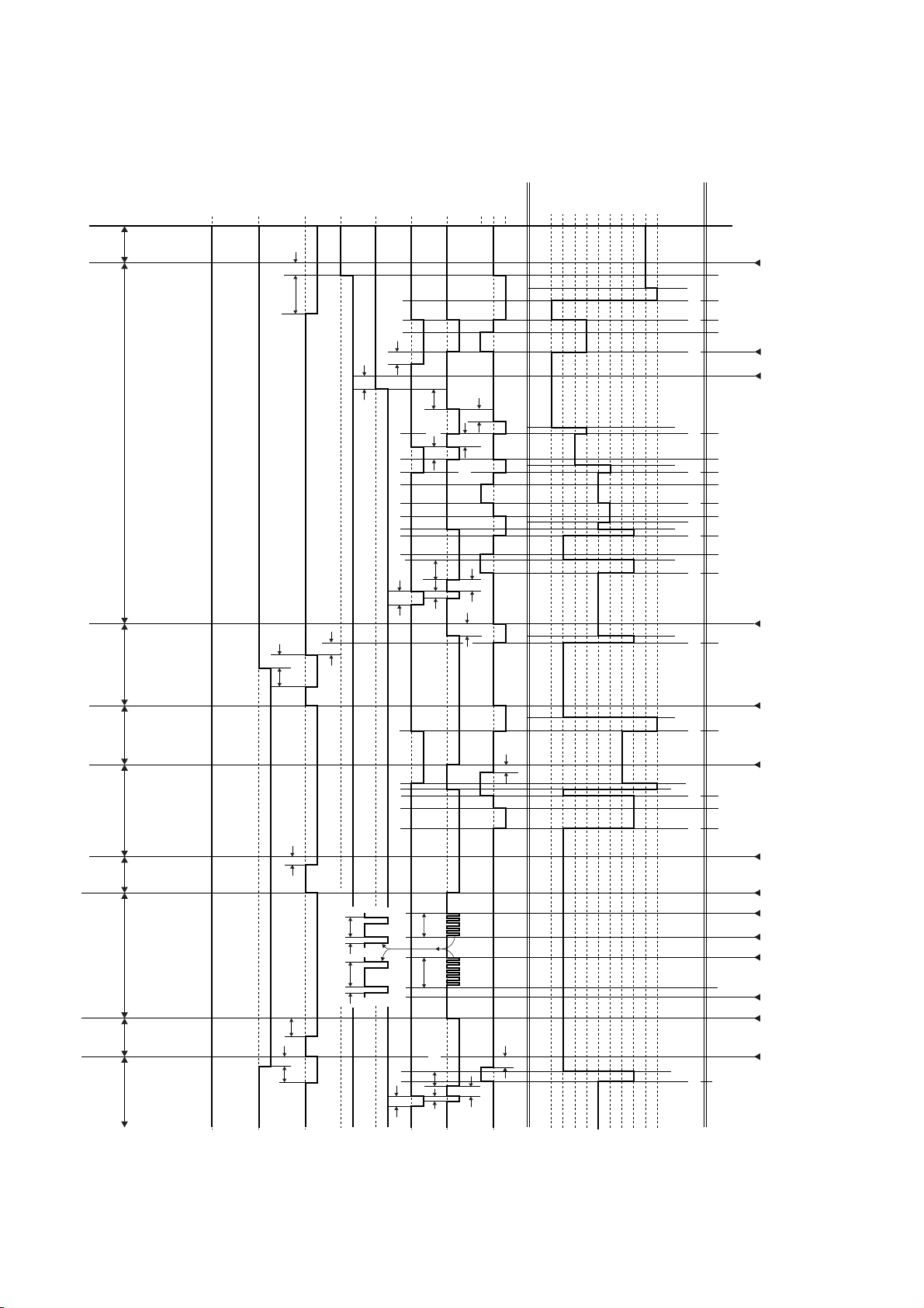
Chart 1
DISPLAY
SYSTEM CONTROL TIMING CHARTS
LD-CONT
44
D-REC-H
D-PB-H
65
A-MUTE-H
31
P-ON
ROTATION
DRUM
66
C-F/R
C-DRIVE
82
CL/SS
EJ
AU
RS
SF
SM
TL
FB
AL
SB
1
LD-SW
PIN NO.
1. EJECT (POWER OFF) -> CASSETTE IN (POWER ON) -> STOP(B) -> STOP(A) -> PLAY -> RS -> FS -> PLAY -> STILL(N-CANCEL) -> PLAY -> STOP(A)
-OFF
POWER
STOP
PLAY RS
0.2S
after channel setting
+620mS(PAL)
+100mS(NTSC)
0.2S
0.3S
0.8S
ON
0.2S
ON
0.2S
40mS
1.2S
0.2S
0.4S
20mS
"Z"
0.2S
0.2S
0.2S
0.2S
TL
SF
AU
AU
AU
CLEJ
SB
TL SB
FB
SM
SM
SMSF AL AL RS AU AL SM
EJECT
CASS.LOAD
LD-FWD
0.2S
LD-REV
STOP(B)
LD-FWD
0.4S
LD-FWD
0.2S
LD-REV
0.2S
LD-FWD
0.5S
LD-REV
STOP(A)
LD-FWD
PLAY
ST-S
"OFF"
REC
SFT-SW
POWER
PLAY
SS
LD-FWD
0.3S
FS
1.0S
PLAY STILL STOPPLAY
SP MODE
>5.0S 5.0S
6mS 6mS240mS80mSNTSC
6mS 6mS160mS80mSPA L
1.0S
0.12S
0.8S
LP/SLP MODE
40mS
20mS0.4S
0.3S
0.2S
RS1(RS2)
SS
LD-REV
AL AU
0.2S
LD-FWD
FS1(FS2)
PLAY
STILL
NOISE
CANCEL
STILL
NOISE
CANCEL
STILL
PLAY
LD-REV
STOP(A)
REW
FF
PLAY
PAUSE
PAUSE
ON
PAUSE
OFF
PAUSE
ON
PAUSE
OFF
PLAY
STOP
/EJECT
1-13-1 Z13P2HTI
Page 55
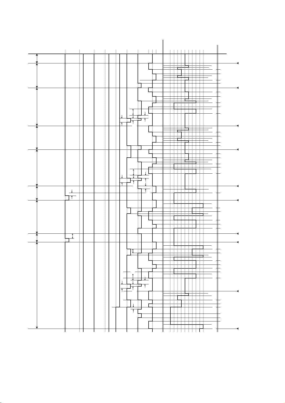
Chart 2
DISPLAY
44
D-REC-H
D-PB-H
31
65
P-ON
A-MUTE-H
ROTATION
DRUM
66
C-F/R
C-DRIVE
LD-CONT
82
SB
PIN NO.
1
EJ
AU
RS
SF
SM
TL
FB
AL
CL/SS
LD-SW
2. STOP(A) -> FF -> STOP(A) -> REW -> STOP(A) -> REC -> PAUSE -> PAUSE or REC -> STOP(A) -> EJECT
STOP
STOPFF
REW STOP
REC
RECREC PAUSE STOP
1.0S
1.2S
ON
ON
40mS
40mS
40mS
0.4S
20mS
0.4S
20mS
1.5S(NTSC)
1.0S(PAL)
0.4S
"Z"
0.2S
0.2S
0.2S
SM SF FB SM AU AU SS
FB SF AU AUFB SF
TL TL SMSM SF SFAL AL SM AL AL ALAU AU SM TL SB EJRS RSSM
SF FB SM
AU
SS SS SF
AL AL AUSS FB CL
STOP(A)
LD-REV
0.2S
LD-FWD
0.2S
FF
REV
1.0S
LD-FWD
0.5S
LD-REV
STOP(A)
LD-REV
0.2S
LD-FWD
0.2S
REW
LD-REV
1.0S
LD-FWD
0.5S
LD-REV
STOP(A)
LD-FWD
REC
LD-FWD
2.5S Short REV
LD-REV
0.2S
LD-FWD
REC PAUSE
REC
LD-FWD
1.5S
LD-REV
0.2S
LD-FWD
0.5S
LD-REV
FF
STOP
/EJECT
REW
STOP
/EJECT
REC
PAUSE
REC or
PAUSE
STOP
/EJECT
20mS
0.1S
0.2S
STOP(A)
LD-REV
0.2S
LD-REV
0.5S
0.2S
0.5S
CASS. UNLD
EJECT
STOP
/EJECT
ST-S
"ON"
1-13-2 Z13P2HTI
Page 56
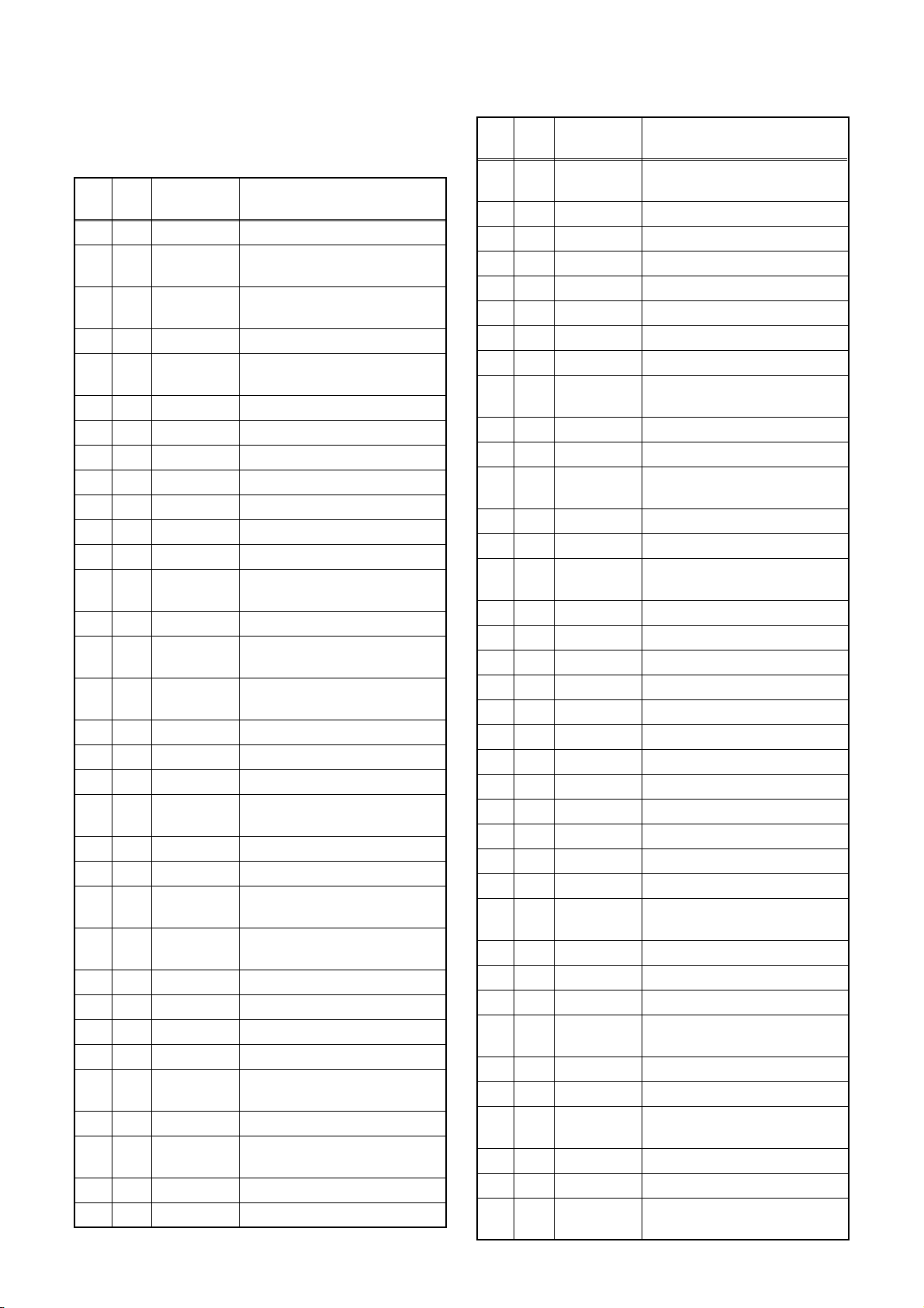
IC PIN FUNCTION DESCRIPTIONS
IC201 (TV/VCR Micro Controller IC)
“H” ≥ 4.5 V, “L” ≤ 1.0 V
Pin
IN/
No.
OUT
1 - NU Not Used
2IN
3IN
4 IN END-SENS End-Sensor
5INAFC
6 IN V-ENV Video Envelope Input
7 IN KEY-1 Key 1 Input
8 IN KEY-2 Key 2 Input
9 IN LD-SW Loading Switch Input
10 IN ST-SENS Start-Sensor
11 - NU Not Used
12 - NU Not Used
IN/
13
OUT
14 IN REMOTE Remote Signal Input
15 OUT C-ROTA
16 OUT H-A-SW
17 - NU Not Used
18 OUT RF-SW Video Head Switching Pulse
19 - NU Not Used
20 OUT A-MUTE-H
21 - NU Not Used
22 - NU Not Used
IN/
23
OUT
IN/
24
OUT
25 - NU Not Used
26 - NU Not Used
27 - NU Not Used
28 - NU Not Used
29 OUT
30 - NU Not Used
31 IN
32 - NU Not Used
33 - NU Not Used
Signal
Name
P-SAFETY 2Power Supply Failure
Detection 2
P-SAFETY 1Power Supply Failure
Detection 1
Automatic Frequency Control
Signal
DV SYNC Artificial V-Sync Output
Color Phase Rotary
Changeover SIgnal
Video Head Amp Switching
Pulse
Audio Mute Control Signal
(Mute = “H”)
REC-LED
REC-LED
SCARTMUTE
RECSAFETY
Recording LED Control
Signal
Recording LED Control
Signal
RAPID-Switch Input Signal
from Scart Jack
Record Protection Tab
Detection
Function
Pin
IN/
No.
OUT
34 IN RESET
35 IN XCIN Sub Clock 32 kHz
36 OUT XCOUT Sub Clock 32 kHz
37 - TIMER+5V Vcc
38 IN XIN Main Clock Input
39 OUT XOUT Main Clock Output
40 - GND GND
41 OUT SPOT-KILL Counter-measure for Spot
42 OUT EXT-L
43 IN CLKSEL Clock Select (GND)
44 OUT SP-MUTE Speaker Mute Signal
IN/
45
OUT
46 - GND GND
47 OUT D-REC-H Delayed Record Signal
48 OUT SCART-H
49 - OSD-GND OSD GND
50 - NU Not Used
51 - NU Not Used
52 - NU Not Used
53 - OSDVcc OSDVcc
54 - HLF HLF
55 - NU Not Used
56 IN CV-IN Video Signal Input
57 - GND GND
58 IN H-SYNC H-SYNC Input
59 IN V-SYNC V-SYNC Input
60 OUT OSD-BLK Output for Picture Cut off
61 OUT
62 OUT OSD-B Blue Output
63 OUT OSD-G Green Output
64 OUT OSD-R Red Output
65 IN
66 - NU Not Used
67 OUT P-ON-H Power On Signal at High
68 IN
69 - NU Not Used
70 OUT TEXT-IN-H Tele Text Input Signal at High
71 OUT SCL
Signal
Name
I2C-OPEN
RGBCONT
RAPIT-SWIN
SLOW-SWIN
Function
System Reset Signal (Reset
= “L”)
External Input or Playback =
Output
White Balance Adjust Mode
Judgment
Switching Signal of Scart
Jack and RCA Jack
RGB Control Signal
RAPID-Switch Input Signal
Slow Switch Input Signal
E2PROM/CHROMA IC Tuner
Communication Clock
1-14-1 T6609PIN
Page 57
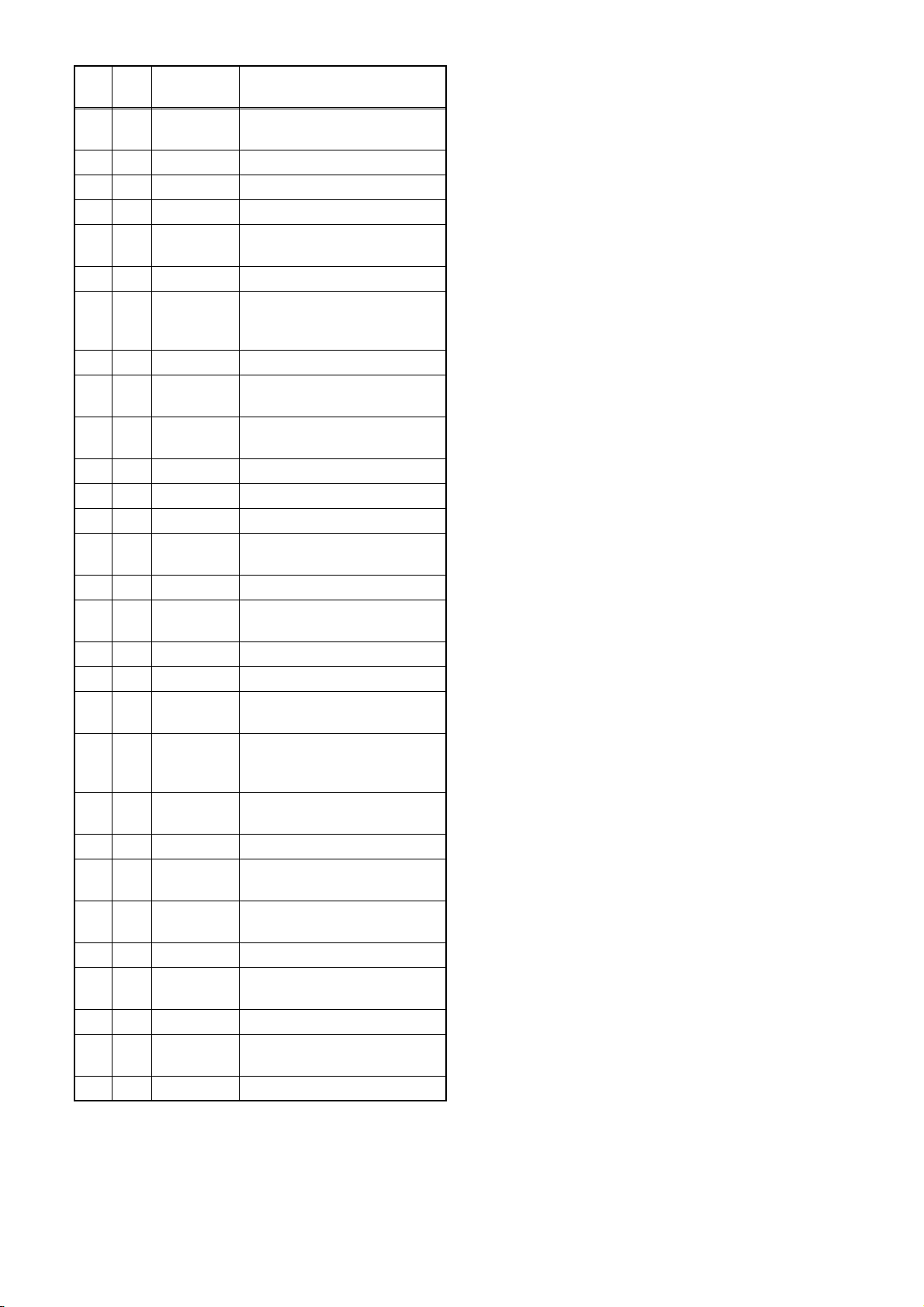
Pin
IN/
No.
OUT
IN/
72
OUT
73 - NU Not Used
74 IN C-SYNC C-Sync Input
75 - NU Not Used
76 OUT C-CONT
77 OUT D-CONT Drum Motor Control Signal
78 OUT C-F/R
79 - NU Not Used
IN/
80
OUT
IN/
81
OUT
82 OUT TEXT-L Teletext Control Signal
83 - NU Not Used
84 - NU Not Used
85 IN P-DOWN-L
86 - NU Not Used
87 IN C-FG
88 - AMPVss AMPVss (GND)
89 - NU Not Used
90 IN D-PFG
91 OUT
92 IN
93 - C C Terminal
IN/
94
OUT
IN/
95
OUT
96 - AMPC AMPC
97 OUT
98 - AMPVcc AMPVcc
99 - AVcc
100 IN AGC Tuner IF Output Signal
Signal
Name
SDA
T- R E E L
LD-CONT Loading Motor Control Signal
AMP
VREFOUT
AMP
VREF- IN
CTL (-) CTL (-)
CTL (+) CTL (+)
CTL AMPOUT
E2PROM/CHROMA IC Tuner
Communication Data
Capstan Motor Control
Signal
Capstan Motor FWD/REV
Control Signal (FWD = “L”/
REV = “H”)
Take Up Reel Rotation
Signal
Power Voltage Down
Detector Signal at Low
Capstan Motor Rotation
Detection Pulse
Drum Motor Phase/
Frequency Generator
Standard Voltage Output
Standard Voltage Input
Control Amp Output
A/D Converter Power Input/
Standard Voltage Input
Function
1-14-2 T6609PIN
Page 58
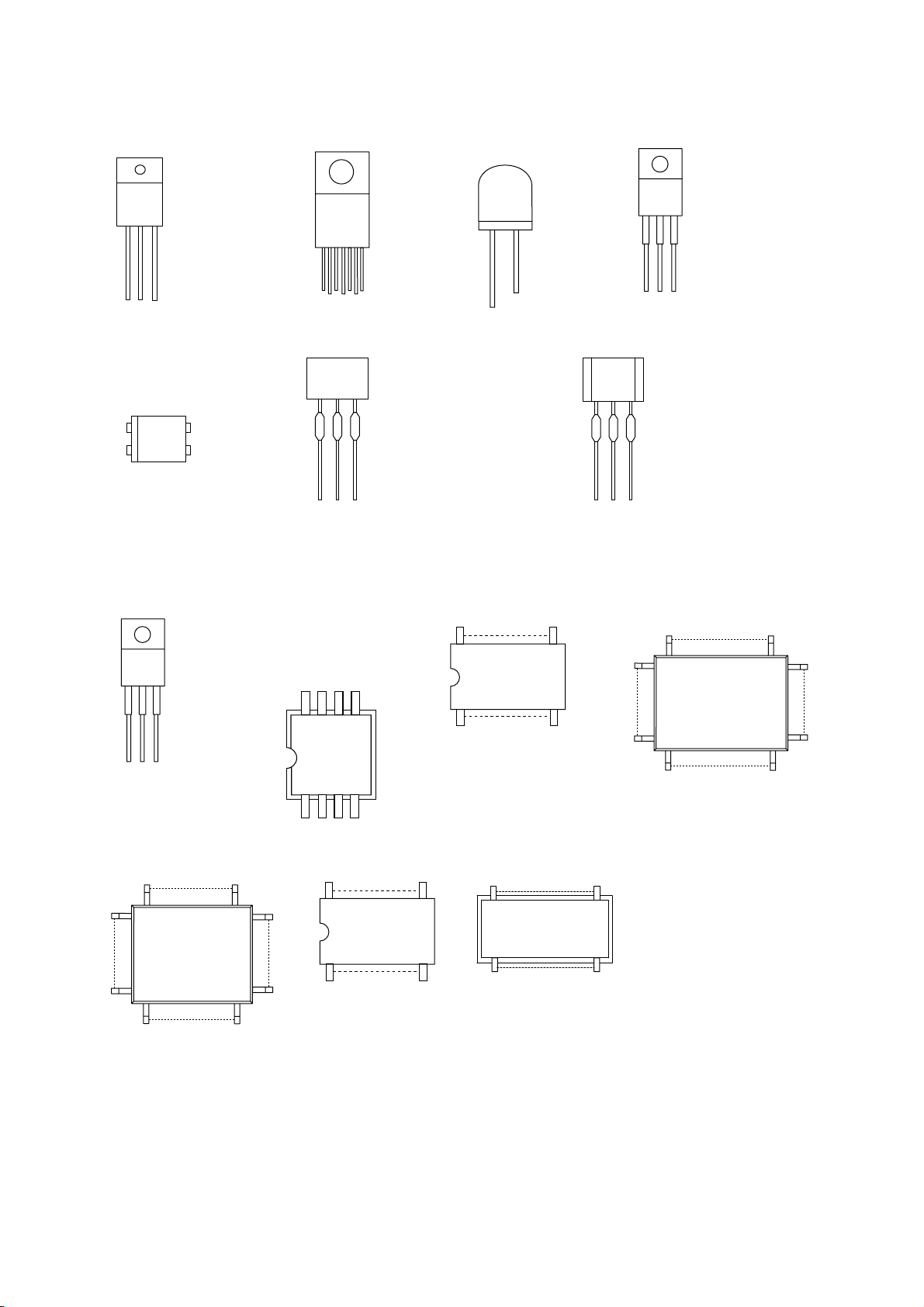
LEAD IDENTIFICATIONS
2SK2647
S: Souce
D: Drain
G: Gate
S D G
PS2561L1-1-VL
PS2561L1-1-VW
1
2
KA7805A
KIA7805API
UA7805CKCE3
LA78040A
MID-32A22F
PT204-6B-12
2SC5884000RF
2SD1913(R)
KTC2026Y
TT2084LS-YB11
TT2138LS-YB11
E C B
B C E
2SA1015-GR(TE2 F T)
2SA1175(F)
2SA950(Y,O)
2SC1627Y-TPE2
2SC2482 TPE6
2SC2785(F,H,J)
2SC3468(D,E)-AE
BN1F4M-T
KTA1267-GR-AT/P
KTA1271(Y)
KTC3198-GR-AT/P
KTC3199-GR-AT/P
LA71750EM-MPB-E
M3776AMCA-BA7GP
80
51
IN G OUT
C
E
2SA1346
2SC1815-GR(TE2 F T)
2SC2120-O(TE2 F T)
1: A
4
2: K
3
3: E
4: C
E C B
AT24C04N-10SC
BR24C04F
BR24C04F-W
BR24L04F-WE2
CAT24WC04JI
2SC2120-Y(TE2 F T)
2SC3331(T,U)
KRA103M-AT/P
KTA-1266-GR-AT/P
KTC3203-Y-AT/P
KTC3207
CD4053BCSJX
CD4053BNSR
TC4053BF(N)
16
9
M24C04-MN6
M24C04-WMN6P
M24C04-WMN6TP
81
50
123
M61209BFP R60T
48
49
64
1
1: IN
2: GND
3: OUT
33
16
17
32
52
5
4
SAA5265
27
1
8
100
1
31
30
LA4224
8
5
8
1
1
26
1
4
1-15-1 T6609LE
Page 59
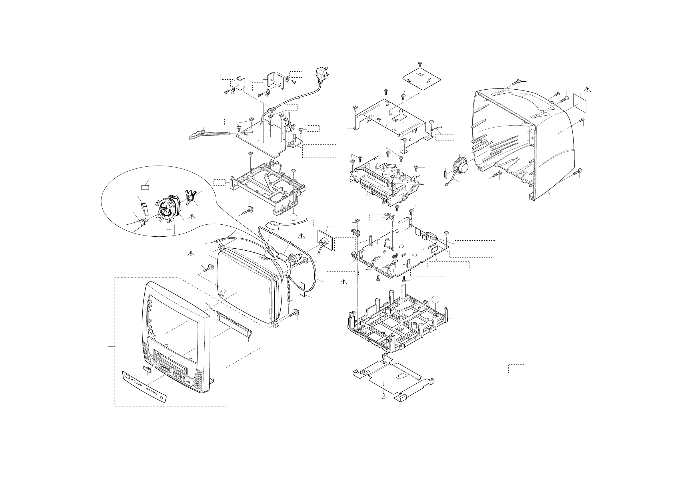
Cabinet
EXPLODED VIEWS
L9
Details for L551
and surrounding parts
V501-2
SHINWHA
TAPE SGT-730
(WHITE)
SHINWHA
TAPE SGT-730
(BLACK)
V501-3
A12
V501-1
L551
CLN551
V501
B2
PL2
PB1
PB5
PL1
L8
B2
PB4
PL2
PL2
PL1
A
L551
PL1
H.V./Power
Supply CBA
L8
CRT CBA
B2
DG601
TL1
TB2
TL1
TL1
TB10
Sensor
CBA
Main CBA
1B1
TB3
TB21
TB7
TL14
Scotch Tape
TL1
TL1
TL1
TL1
TL1
Sensor CBA
TL18
B3
TL1
CL604
SP151
B10
TL1
TL1
TL1
Junction B CBA
Junction C CBA
Junction A CBA
CL801
L1
L1
A2
L2
L1
A3
L2
L1
A1X
A1-2
A1-3
A1-1
A1-5
A1-4
B1
B2
Scotch
Tape #880
TL14
A
TB23
TB1
See Electrical Parts List
for parts with this mark.
Some Ref. Numbers are
not in sequence.
1-16-1 T6609CEX
Page 60
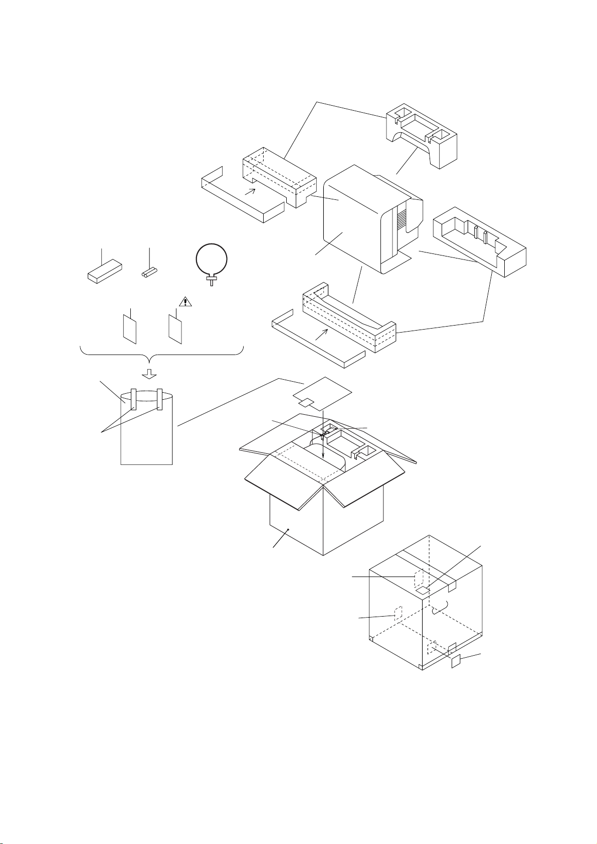
Packing
S2
X1
TAPE
X3
X4
Loop Antenna
S6
X2X24
S3
TAPE
S12
(IC Tag Label)
S1
(Shipping Label)
FRONT
S5
S4
1-16-2 T6609PEX
Page 61
MECHANICAL PARTS LIST
PRODUCT SAFETY NOTE: Products marked with a
! have special characteristics important to safety.
Before replacing any of these components, read carefully the product safety notice in this service manual.
Don't degrade the safety of the product through
improper servicing.
NOTE:
Parts that are not assigned part numbers (---------) are
not available.
Ref. No. Description Part No.
A1X FRONT CABINET ASSEMBLY T6609BK 1EM120133
A2 REAR CABINET T6600EA 0EM000864
A3! RATING LABEL T6609BK 1EM420776
A12 POWER BUTTON T6600EA 0EM302029
A1-1 FRONT CABINET T6605VF 0EM000936
A1-2 CONTROL PLATE T6605VF 0EM201851
A1-3 BRAND BADGE T6609BK 1EM420733
A1-4 CASSETTE DOOR T6600EA 0EM408804
A1-5 SPRING DOOR(Z10) T5200UA 0EM406687
1B1 DECK ASSEMBLY CZD013/VM2326 or N2326FT
DECK ASSEMBLY CZD014/VM2526 N2526FT
B1 SPRING TENSION B0080B0 EM40808 26WH006
B2 M5 CRT SCREW(B) B4000UA 0VM403923
B3 SHIELD PLATE (PAL 14V) T6600EA 0EM408803
B10 CLOTH(10X30XT0.5) B5900UA 0EM404486
CL801 WIRE ASSEMBLY (SPEAKER) 2P/200 WX1T6300-002
CLN551 CRT GND WIRE WX1L7720-001
DG601!DEGAUSSING COIL F-056 LLBH00ZTM056
Ref. No. Description Part No.
DRY BATTERY(SUNRISE) R6SSE/2S or XB0M451MS002
DRY BATTERY R6P/2S XB0M451T0001
X24 QUICK USERS GUIDE T6609BK 1EMN20245
L1 SCREW P-TIGHT 4X18 BIND HEAD + GBMP4180
L2 SCREW P-TIGHT M4X12 BIND HEAD+ GBUP4120
L8 FLAT HEAD SCREW T4000UA 0EM404793
L9 SCREW S-TIGHT 3X4 BIND HEAD+ GBMS3040
L551! DEFLECTION YOKE LLBY00ZSY005 or LLBY00ZSY005
! DEFLECTION YOKE KDY3GDA82X LLBY00ZMS011
SP151 SPEAKER S08F02B or DSD0808XQ010
SPEAKER J-F097-C5 DSD0808DCP01
TB1 TRAY CHASSIS T6400RA 0EM000697
TB2 TOP COVER T6300RA 0EM101155
TB10 RCA HOLDER T6400RA 0EM407753
TB23 BOTTOM PLATE T6300RA 0EM101156
TL1 SCREW P-TIGHT 3X12 WASHER HEAD+ GCMP3120
TL18 SCREW P-TIGHT M3X8 BIND HEAD+ GBCP3080
TL14 SCREW B-TIGHT D3X8 BIND HEAD+ GBMB3080
V501! CRT A34AGT13X TCRT190CP036
V501-1 C.P.MAGNET JH225-FN-00 XM04000BV003
V501-2 WEDGE FT-00110W or XV10000T4001
WEDGE DB25SR XV10000D9001
V501-3 RUBBER MAGNET 20X10X1.2 XM05000BV001
PACKING
S1 CARTON T6609BK 1EM420774
S2 STYROFOAM TOP ASSEMBLY T6600EA 0EM409185
S3 STYROFOAM BOTTOM ASSEMBLY T6600EA 0EM409186
S4 SERIAL NO. LABEL T6609BK 1EM420775
S5 TUC LABEL T6609BK 1EM421439
S6 SET SHEET B5506UG 800X1500 0EM402369
S12 AC CORD SHEET 0EM407920
ACCESSORIES
X1 BAG POLYETHYLENE 235X365XT0.03 0EM408420
X2! OWNERS MANUAL T6609BK~EN~ 1EMN20244
X3 REMOTE CONTROL 512/ERC001/NE602RD NE602RD
X4 DRY BATTERY R6P UM3 or XB0M451GH001
DRY BATTERY R6P(AR)2PX or XB0M451HU002
DRY BATTERY R6P(AR)2P X ICI or XB0M451HU003
20050601 1-17-1 T6609CA
Page 62
ELECTRICAL PARTS LIST
PRODUCT SAFETY NOTE: Products marked with a
! have special characteristics important to safety.
Before replacing any of these components, read carefully the product safety notice in this service manual.
Don't degrade the safety of the product through
improper servicing.
NOTES:
1. Parts that are not assigned part numbers (---------)
are not available.
2. Tolerance of Capacitors and Resistors are noted
with the following symbols.
C.....±0.25% D.....±0.5% F.....±1%
G.....±2% J......±5% K.....±10%
M.....±20% N.....±30% Z.....+80/-20%
MMA CBA
Ref. No. Description Part No.
MMA CBA
Consists of the following:
MAIN CBA
JUNCTION A CBA
JUNCTION B CBA
JUNCTION C CBA
SENSOR CBA
MAIN CBA
Ref. No. Description Part No.
MAIN CBA
Consists of the following:
CAPACITORS
C001 CHIP CERAMIC CAP.(MELF) F Z 0.01µF/16V or CZM1CZ30F103
CHIP CERAMIC CAP.(MELF) F Z 0.01µF/16V CZM1CZB0F103
C002 ELECTROLYTIC CAP. 47µF/25V M or CE1EMASDL470
ELECTROLYTIC CAP. 47µF/25V M CE1EMASTL470
C006 ELECTROLYTIC CAP. 1µF/50V M or CE1JMASDL010
ELECTROLYTIC CAP. 1µF/50V M or CE1JMASDL1R0
ELECTROLYTIC CAP. 1µF/50V M CE1JMASTL1R0
C008 ELECTROLYTIC CAP. 1µF/50V M or CE1JMASDL010
ELECTROLYTIC CAP. 1µF/50V M or CE1JMASDL1R0
ELECTROLYTIC CAP. 1µF/50V M CE1JMASTL1R0
C009 PCB JUMPER D0.6-P5.0 JW5.0T
C151 ELECTROLYTIC CAP. 330µF/16V M or CE1CMASDL331
ELECTROLYTIC CAP. 330µF/16V M CE1CMASTL331
C152 CERAMIC CAP.(AX) X M 2200pF/16V CCA1CMT0X222
C154 ELECTROLYTIC CAP. 470µF/16V M or CE1CMASDL471
ELECTROLYTIC CAP. 470µF/16V M CE1CMASTL471
C155 ELECTROLYTIC CAP. 0.22µF/50V M H7 CE1JMAVSLR22
C156 CHIP CERAMIC CAP.(1608) B K 4700pF/50V or CHD1JK30B472
CHIP CERAMIC CAP. B K 4700pF/50V CHD1JKB0B472
C157 ELECTROLYTIC CAP. 10µF/25V M H7 CE1EMAVSL100
C160 CHIP CERAMIC CAP.(1608) CH J 270pF/50V or CHD1JJ3CH271
CHIP CERAMIC CAP. CH J 270pF/50V CHD1JJBCH271
C203 CHIP CERAMIC CAP.(MELF) F Z 0.01µF/16V or CZM1CZ30F103
CHIP CERAMIC CAP.(MELF) F Z 0.01µF/16V CZM1CZB0F103
C205 CHIP CERAMIC CAP.(MELF) F Z 0.01µF/16V or CZM1CZ30F103
CHIP CERAMIC CAP.(MELF) F Z 0.01µF/16V CZM1CZB0F103
C207 ELECTROLYTIC CAP. 1µF/50V M H7 CE1JMAVSL1R0
C208 CHIP CERAMIC CAP.(MELF) F Z 0.01µF/16V or CZM1CZ30F103
CHIP CERAMIC CAP.(MELF) F Z 0.01µF/16V CZM1CZB0F103
C209 CHIP CERAMIC CAP.(1608) CH J 22pF/50V or CHD1JJ3CH220
CHIP CERAMIC CAP. CH J 22pF/50V CHD1JJBCH220
0ESA06014
----------
----------
----------
---------0ESA06133
----------
Ref. No. Description Part No.
C210 CHIP CERAMIC CAP.(1608) CH J 22pF/50V or CHD1JJ3CH220
CHIP CERAMIC CAP. CH J 22pF/50V CHD1JJBCH220
C211 ELECTROLYTIC CAP. 47µF/6.3V M H7 CE0KMAVSL470
C212 CHIP CERAMIC CAP.(MELF) F Z 0.01µF/16V or CZM1CZ30F103
CHIP CERAMIC CAP.(MELF) F Z 0.01µF/16V CZM1CZB0F103
C213 ELECTROLYTIC CAP. 47µF/6.3V M H7 CE0KMAVSL470
C214 ELECTROLYTIC CAP. 330µF/6.3V M or CE0KMASDL331
ELECTROLYTIC CAP. 330µF/6.3V M CE0KMASTL331
C217 CHIP CERAMIC CAP.(1608) CH D 10pF/50V or CHD1JD3CH100
CHIP CERAMIC CAP. CH D 10pF/50V CHD1JDBCH100
C218 CHIP CERAMIC CAP.(1608) CH D 10pF/50V or CHD1JD3CH100
CHIP CERAMIC CAP. CH D 10pF/50V CHD1JDBCH100
C221 ELECTROLYTIC CAP. 47µF/6.3V M H7 CE0KMAVSL470
C222 CHIP CERAMIC CAP.(MELF) F Z 0.01µF/16V or CZM1CZ30F103
CHIP CERAMIC CAP.(MELF) F Z 0.01µF/16V CZM1CZB0F103
C223 CHIP CERAMIC CAP.(MELF) Y K 4700pF/16V or CZM1CK30Y472
CHIP CERAMIC CAP.(MELF) Y K 4700pF/16V CZM1CKB0Y472
C224 CHIP CERAMIC CAP.(1608) F Z 0.1µF/50V or CHD1JZ30F104
CHIP CERAMIC CAP.(1608) F Z 0.1µF/25V or CHD1EZ30F104
CHIP CERAMIC CAP. F Z 0.1µF/50V or CHD1JZB0F104
CHIP CERAMIC CAP. F Z 0.1µF/25V CHD1EZB0F104
C225 CHIP CERAMIC CAP. CH J 560pF/50V or CHD1JJ3CH561
CHIP CERAMIC CAP. CH J 560pF/50V CHD1JJBCH561
C226 CHIP CERAMIC CAP.(1608) F Z 0.1µF/50V or CHD1JZ30F104
CHIP CERAMIC CAP.(1608) F Z 0.1µF/25V or CHD1EZ30F104
CHIP CERAMIC CAP. F Z 0.1µF/50V or CHD1JZB0F104
CHIP CERAMIC CAP. F Z 0.1µF/25V CHD1EZB0F104
C227 CHIP CERAMIC CAP.(1608) CH D 10pF/50V or CHD1JD3CH100
CHIP CERAMIC CAP. CH D 10pF/50V CHD1JDBCH100
C228 CHIP CERAMIC CAP.(1608) CH D 10pF/50V or CHD1JD3CH100
CHIP CERAMIC CAP. CH D 10pF/50V CHD1JDBCH100
C229 CHIP CERAMIC CAP.(1608) B K 0.022µF/50V or CHD1JK30B223
CHIP CERAMIC CAP.(1608) B K 0.022µF/25V or CHD1EK30B223
CHIP CERAMIC CAP. B K 0.022µF/50V or CHD1JKB0B223
CHIP CERAMIC CAP. B K 0.022µF/25V CHD1EKB0B223
C230 CHIP CERAMIC CAP.(1608) F Z 0.1µF/50V or CHD1JZ30F104
CHIP CERAMIC CAP.(1608) F Z 0.1µF/25V or CHD1EZ30F104
CHIP CERAMIC CAP. F Z 0.1µF/50V or CHD1JZB0F104
CHIP CERAMIC CAP. F Z 0.1µF/25V CHD1EZB0F104
C231 CHIP CERAMIC CAP.(MELF) F Z 0.01µF/16V or CZM1CZ30F103
CHIP CERAMIC CAP.(MELF) F Z 0.01µF/16V CZM1CZB0F103
C233! CHIP CERAMIC CAP.(MELF) Y K 1000pF/35V or CZM1GK30Y102
! CHIP CERAMIC CAP.(MELF) Y K 1000pF/35V CZM1GKB0Y102
C234 CHIP CERAMIC CAP.(1608) B K 0.01µF/50V or CHD1JK30B103
CHIP CERAMIC CAP. B K 0.01µF/50V CHD1JKB0B103
C235 ELECTROLYTIC CAP. 47µF/6.3V M H7 CE0KMAVSL470
C236 CHIP CERAMIC CAP.(1608) F Z 0.1µF/50V or CHD1JZ30F104
CHIP CERAMIC CAP.(1608) F Z 0.1µF/25V or CHD1EZ30F104
CHIP CERAMIC CAP. F Z 0.1µF/50V or CHD1JZB0F104
CHIP CERAMIC CAP. F Z 0.1µF/25V CHD1EZB0F104
C237 ELECTROLYTIC CAP. 47µF/6.3V M H7 CE0KMAVSL470
C238 CHIP CERAMIC CAP.(1608) F Z 0.1µF/50V or CHD1JZ30F104
CHIP CERAMIC CAP.(1608) F Z 0.1µF/25V or CHD1EZ30F104
CHIP CERAMIC CAP. F Z 0.1µF/50V or CHD1JZB0F104
CHIP CERAMIC CAP. F Z 0.1µF/25V CHD1EZB0F104
C239 CHIP CERAMIC CAP. CH J 560pF/50V or CHD1JJ3CH561
CHIP CERAMIC CAP. CH J 560pF/50V CHD1JJBCH561
C240 CHIP CERAMIC CAP.(MELF) Y K 4700pF/16V or CZM1CK30Y472
CHIP CERAMIC CAP.(MELF) Y K 4700pF/16V CZM1CKB0Y472
C241 ELECTROLYTIC CAP. 22µF/50V M or CE1JMASDL220
ELECTROLYTIC CAP. 22µF/50V M CE1JMASTL220
C242 CHIP CERAMIC CAP.(MELF) F Z 0.01µF/16V or CZM1CZ30F103
CHIP CERAMIC CAP.(MELF) F Z 0.01µF/16V CZM1CZB0F103
20050601 1-18-1 T6609EL
Page 63
Ref. No. Description Part No.
C243 ELECTROLYTIC CAP. 47µF/6.3V M H7 CE0KMAVSL470
C244 CHIP CERAMIC CAP.(MELF) F Z 0.01µF/16V or CZM1CZ30F103
CHIP CERAMIC CAP.(MELF) F Z 0.01µF/16V CZM1CZB0F103
C245 ELECTROLYTIC CAP. 47µF/6.3V M H7 CE0KMAVSL470
C248 ELECTROLYTIC CAP. 47µF/6.3V M H7 CE0KMAVSL470
C253 CHIP CERAMIC CAP.(1608) B K 0.01µF/50V or CHD1JK30B103
CHIP CERAMIC CAP. B K 0.01µF/50V CHD1JKB0B103
C254 CHIP CERAMIC CAP. CH J 560pF/50V or CHD1JJ3CH561
CHIP CERAMIC CAP. CH J 560pF/50V CHD1JJBCH561
C255 CHIP CERAMIC CAP. CH J 560pF/50V or CHD1JJ3CH561
CHIP CERAMIC CAP. CH J 560pF/50V CHD1JJBCH561
C256 ELECTROLYTIC CAP. 10µF/25V M H7 CE1EMAVSL100
C301 CHIP CERAMIC CAP.(MELF) F Z 0.01µF/16V or CZM1CZ30F103
CHIP CERAMIC CAP.(MELF) F Z 0.01µF/16V CZM1CZB0F103
C302 ELECTROLYTIC CAP. 470µF/6.3V M or CE0KMASDL471
ELECTROLYTIC CAP. 470µF/6.3V M CE0KMASTL471
C303 CHIP CERAMIC CAP.(1608) B K 0.01µF/50V or CHD1JK30B103
CHIP CERAMIC CAP. B K 0.01µF/50V CHD1JKB0B103
C304 CHIP CERAMIC CAP.(1608) B K 0.01µF/50V or CHD1JK30B103
CHIP CERAMIC CAP. B K 0.01µF/50V CHD1JKB0B103
C305 ELECTROLYTIC CAP. 1µF/50V M or CE1JMASDL010
ELECTROLYTIC CAP. 1µF/50V M or CE1JMASDL1R0
ELECTROLYTIC CAP. 1µF/50V M CE1JMASTL1R0
C307 CHIP CERAMIC CAP.(1608) F Z 0.1µF/50V or CHD1JZ30F104
CHIP CERAMIC CAP.(1608) F Z 0.1µF/25V or CHD1EZ30F104
CHIP CERAMIC CAP. F Z 0.1µF/50V or CHD1JZB0F104
CHIP CERAMIC CAP. F Z 0.1µF/25V CHD1EZB0F104
C308 CHIP CERAMIC CAP.(1608) F Z 0.1µF/50V or CHD1JZ30F104
CHIP CERAMIC CAP.(1608) F Z 0.1µF/25V or CHD1EZ30F104
CHIP CERAMIC CAP. F Z 0.1µF/50V or CHD1JZB0F104
CHIP CERAMIC CAP. F Z 0.1µF/25V CHD1EZB0F104
C309 FILM CAP.(P) 0.1µF/50V J or CMA1JJS00104
FILM CAP.(P) 0.1µF/50V J CA1J104MS029
C310 CHIP CERAMIC CAP.(1608) F Z 0.1µF/50V or CHD1JZ30F104
CHIP CERAMIC CAP.(1608) F Z 0.1µF/25V or CHD1EZ30F104
CHIP CERAMIC CAP. F Z 0.1µF/50V or CHD1JZB0F104
CHIP CERAMIC CAP. F Z 0.1µF/25V CHD1EZB0F104
C311 ELECTROLYTIC CAP. 470µF/6.3V M or CE0KMASDL471
ELECTROLYTIC CAP. 470µF/6.3V M CE0KMASTL471
C312 CHIP CERAMIC CAP.(MELF) B K 180pF/50V or CZM1JK30B181
CHIP CERAMIC CAP.(MELF) B K 180pF/50V CZM1JKB0B181
C313 CHIP CERAMIC CAP.(1608) F Z 0.1µF/50V or CHD1JZ30F104
CHIP CERAMIC CAP.(1608) F Z 0.1µF/25V or CHD1EZ30F104
CHIP CERAMIC CAP. F Z 0.1µF/50V or CHD1JZB0F104
CHIP CERAMIC CAP. F Z 0.1µF/25V CHD1EZB0F104
C314 CHIP CERAMIC CAP.(1608) B K 0.01µF/50V or CHD1JK30B103
CHIP CERAMIC CAP. B K 0.01µF/50V CHD1JKB0B103
C315 CHIP CERAMIC CAP.(1608) F Z 0.1µF/50V or CHD1JZ30F104
CHIP CERAMIC CAP.(1608) F Z 0.1µF/25V or CHD1EZ30F104
CHIP CERAMIC CAP. F Z 0.1µF/50V or CHD1JZB0F104
CHIP CERAMIC CAP. F Z 0.1µF/25V CHD1EZB0F104
C316 ELECTROLYTIC CAP. 1µF/50V M or CE1JMASDL010
ELECTROLYTIC CAP. 1µF/50V M or CE1JMASDL1R0
ELECTROLYTIC CAP. 1µF/50V M CE1JMASTL1R0
C317 CHIP CERAMIC CAP. CH J 150pF/50V or CHD1JJ3CH151
CHIP CERAMIC CAP. CH J 150pF/50V CHD1JJBCH151
C318 ELECTROLYTIC CAP. 1µF/50V M or CE1JMASDL010
ELECTROLYTIC CAP. 1µF/50V M or CE1JMASDL1R0
ELECTROLYTIC CAP. 1µF/50V M CE1JMASTL1R0
C319 ELECTROLYTIC CAP. 1µF/50V M or CE1JMASDL010
ELECTROLYTIC CAP. 1µF/50V M or CE1JMASDL1R0
ELECTROLYTIC CAP. 1µF/50V M CE1JMASTL1R0
C320 CHIP CERAMIC CAP.(1608) B K 0.01µF/50V or CHD1JK30B103
CHIP CERAMIC CAP. B K 0.01µF/50V CHD1JKB0B103
C321 ELECTROLYTIC CAP. 1µF/50V M or CE1JMASDL010
ELECTROLYTIC CAP. 1µF/50V M or CE1JMASDL1R0
Ref. No. Description Part No.
ELECTROLYTIC CAP. 1µF/50V M CE1JMASTL1R0
C322 ELECTROLYTIC CAP. 470µF/10V M or CE1AMASDL471
ELECTROLYTIC CAP. 470µF/10V M CE1AMASTL471
C323 ELECTROLYTIC CAP. 47µF/25V M or CE1EMASDL470
ELECTROLYTIC CAP. 47µF/25V M CE1EMASTL470
C324 CHIP CERAMIC CAP.(MELF) F Z 0.01µF/16V or CZM1CZ30F103
CHIP CERAMIC CAP.(MELF) F Z 0.01µF/16V CZM1CZB0F103
C325 MYLAR CAP. 0.22µF/50V J or CMA1JJS00224
FILM CAP.(P) 0.22µF/50V J or CA1J224MS029
TF CAP. 0.22µF/50V J CT1J224MS045
C326 ELECTROLYTIC CAP. 1µF/50V M or CE1JMASDL010
ELECTROLYTIC CAP. 1µF/50V M or CE1JMASDL1R0
ELECTROLYTIC CAP. 1µF/50V M CE1JMASTL1R0
C327 CHIP CERAMIC CAP.(1608) B K 0.01µF/50V or CHD1JK30B103
CHIP CERAMIC CAP. B K 0.01µF/50V CHD1JKB0B103
C328 MYLAR CAP. 0.22µF/50V J or CMA1JJS00224
FILM CAP.(P) 0.22µF/50V J or CA1J224MS029
TF CAP. 0.22µF/50V J CT1J224MS045
C330 CHIP CERAMIC CAP.(MELF) F Z 0.01µF/16V or CZM1CZ30F103
CHIP CERAMIC CAP.(MELF) F Z 0.01µF/16V CZM1CZB0F103
C331 ELECTROLYTIC CAP. 47µF/10V M or CE1AMASDL470
ELECTROLYTIC CAP. 47µF/10V M CE1AMASTL470
C332 CHIP CERAMIC CAP.(1608) F Z 0.1µF/50V or CHD1JZ30F104
CHIP CERAMIC CAP.(1608) F Z 0.1µF/25V or CHD1EZ30F104
CHIP CERAMIC CAP. F Z 0.1µF/50V or CHD1JZB0F104
CHIP CERAMIC CAP. F Z 0.1µF/25V CHD1EZB0F104
C333 CHIP CERAMIC CAP.(1608) F Z 0.1µF/50V or CHD1JZ30F104
CHIP CERAMIC CAP.(1608) F Z 0.1µF/25V or CHD1EZ30F104
CHIP CERAMIC CAP. F Z 0.1µF/50V or CHD1JZB0F104
CHIP CERAMIC CAP. F Z 0.1µF/25V CHD1EZB0F104
C334 CHIP CERAMIC CAP.(1608) F Z 0.1µF/50V or CHD1JZ30F104
CHIP CERAMIC CAP.(1608) F Z 0.1µF/25V or CHD1EZ30F104
CHIP CERAMIC CAP. F Z 0.1µF/50V or CHD1JZB0F104
CHIP CERAMIC CAP. F Z 0.1µF/25V CHD1EZB0F104
C336 ELECTROLYTIC CAP. 47µF/10V M or CE1AMASDL470
ELECTROLYTIC CAP. 47µF/10V M CE1AMASTL470
C338 CHIP CERAMIC CAP.(MELF) Y K 1000pF/35V or CZM1GK30Y102
CHIP CERAMIC CAP.(MELF) Y K 1000pF/35V CZM1GKB0Y102
C340 CHIP CERAMIC CAP.(MELF) B K 180pF/50V or CZM1JK30B181
CHIP CERAMIC CAP.(MELF) B K 180pF/50V CZM1JKB0B181
C341 CHIP CERAMIC CAP.(MELF) F Z 0.01µF/16V or CZM1CZ30F103
CHIP CERAMIC CAP.(MELF) F Z 0.01µF/16V CZM1CZB0F103
C344 CHIP CERAMIC CAP.(MELF) Y K 1000pF/35V or CZM1GK30Y102
CHIP CERAMIC CAP.(MELF) Y K 1000pF/35V CZM1GKB0Y102
C350 ELECTROLYTIC CAP. 220µF/10V M or CE1AMASDL221
ELECTROLYTIC CAP. 220µF/10V M CE1AMASTL221
C401 CHIP CERAMIC CAP.(1608) B K 0.01µF/50V or CHD1JK30B103
CHIP CERAMIC CAP. B K 0.01µF/50V CHD1JKB0B103
C402 ELECTROLYTIC CAP. 1µF/50V M H7 CE1JMAVSL1R0
C403 ELECTROLYTIC CAP. 1µF/50V M H7 CE1JMAVSL1R0
C404 ELECTROLYTIC CAP. 100µF/6.3V H7 CE0KMAVSL101
C405 CHIP CERAMIC CAP.(1608) F Z 0.1µF/50V or CHD1JZ30F104
CHIP CERAMIC CAP.(1608) F Z 0.1µF/25V or CHD1EZ30F104
CHIP CERAMIC CAP. F Z 0.1µF/50V or CHD1JZB0F104
CHIP CERAMIC CAP. F Z 0.1µF/25V CHD1EZB0F104
C406 CHIP CERAMIC CAP.(1608) F Z 0.1µF/50V or CHD1JZ30F104
CHIP CERAMIC CAP.(1608) F Z 0.1µF/25V or CHD1EZ30F104
CHIP CERAMIC CAP. F Z 0.1µF/50V or CHD1JZB0F104
CHIP CERAMIC CAP. F Z 0.1µF/25V CHD1EZB0F104
C407 CHIP CERAMIC CAP.(1608) B K 0.01µF/50V or CHD1JK30B103
CHIP CERAMIC CAP. B K 0.01µF/50V CHD1JKB0B103
C408 CHIP CERAMIC CAP.(1608) F Z 0.1µF/50V or CHD1JZ30F104
CHIP CERAMIC CAP.(1608) F Z 0.1µF/25V or CHD1EZ30F104
CHIP CERAMIC CAP. F Z 0.1µF/50V or CHD1JZB0F104
CHIP CERAMIC CAP. F Z 0.1µF/25V CHD1EZB0F104
C409 CHIP CERAMIC CAP.(1608) F Z 0.1µF/50V or CHD1JZ30F104
20050601 1-18-2 T6609EL
Page 64
Ref. No. Description Part No.
CHIP CERAMIC CAP.(1608) F Z 0.1µF/25V or CHD1EZ30F104
CHIP CERAMIC CAP. F Z 0.1µF/50V or CHD1JZB0F104
CHIP CERAMIC CAP. F Z 0.1µF/25V CHD1EZB0F104
C410 CHIP CERAMIC CAP.(1608) B K 0.01µF/50V or CHD1JK30B103
CHIP CERAMIC CAP. B K 0.01µF/50V CHD1JKB0B103
C411 CHIP CERAMIC CAP.(1608) B K 0.01µF/50V or CHD1JK30B103
CHIP CERAMIC CAP. B K 0.01µF/50V CHD1JKB0B103
C412 ELECTROLYTIC CAP. 1µF/50V M H7 CE1JMAVSL1R0
C413 CHIP CERAMIC CAP.(1608) B K 0.01µF/50V or CHD1JK30B103
CHIP CERAMIC CAP. B K 0.01µF/50V CHD1JKB0B103
C414 CHIP CERAMIC CAP.(1608) F Z 0.1µF/50V or CHD1JZ30F104
CHIP CERAMIC CAP.(1608) F Z 0.1µF/25V or CHD1EZ30F104
CHIP CERAMIC CAP. F Z 0.1µF/50V or CHD1JZB0F104
CHIP CERAMIC CAP. F Z 0.1µF/25V CHD1EZB0F104
C415 CHIP CERAMIC CAP.(1608) B K 0.01µF/50V or CHD1JK30B103
CHIP CERAMIC CAP. B K 0.01µF/50V CHD1JKB0B103
C416 ELECTROLYTIC CAP. 47µF/6.3V M H7 CE0KMAVSL470
C417 ELECTROLYTIC CAP. 1µF/50V M H7 CE1JMAVSL1R0
C418 ELECTROLYTIC CAP. 1µF/50V M H7 CE1JMAVSL1R0
C419 CHIP CERAMIC CAP.(1608) F Z 0.1µF/50V or CHD1JZ30F104
CHIP CERAMIC CAP.(1608) F Z 0.1µF/25V or CHD1EZ30F104
CHIP CERAMIC CAP. F Z 0.1µF/50V or CHD1JZB0F104
CHIP CERAMIC CAP. F Z 0.1µF/25V CHD1EZB0F104
C420 CHIP CERAMIC CAP.(1608) F Z 0.1µF/50V or CHD1JZ30F104
CHIP CERAMIC CAP.(1608) F Z 0.1µF/25V or CHD1EZ30F104
CHIP CERAMIC CAP. F Z 0.1µF/50V or CHD1JZB0F104
CHIP CERAMIC CAP. F Z 0.1µF/25V CHD1EZB0F104
C421 ELECTROLYTIC CAP. 10µF/25V M H7 CE1EMAVSL100
C424 CHIP CERAMIC CAP.(1608) F Z 0.1µF/50V or CHD1JZ30F104
CHIP CERAMIC CAP.(1608) F Z 0.1µF/25V or CHD1EZ30F104
CHIP CERAMIC CAP. F Z 0.1µF/50V or CHD1JZB0F104
CHIP CERAMIC CAP. F Z 0.1µF/25V CHD1EZB0F104
C425 CHIP CERAMIC CAP.(1608) CH J 68pF/50V or CHD1JJ3CH680
CHIP CERAMIC CAP. CH J 68pF/50V CHD1JJBCH680
C426 CHIP CERAMIC CAP.(1608) F Z 0.1µF/50V or CHD1JZ30F104
CHIP CERAMIC CAP.(1608) F Z 0.1µF/25V or CHD1EZ30F104
CHIP CERAMIC CAP. F Z 0.1µF/50V or CHD1JZB0F104
CHIP CERAMIC CAP. F Z 0.1µF/25V CHD1EZB0F104
C427 CHIP CERAMIC CAP.(1608) F Z 0.1µF/50V or CHD1JZ30F104
CHIP CERAMIC CAP.(1608) F Z 0.1µF/25V or CHD1EZ30F104
CHIP CERAMIC CAP. F Z 0.1µF/50V or CHD1JZB0F104
CHIP CERAMIC CAP. F Z 0.1µF/25V CHD1EZB0F104
C430 ELECTROLYTIC CAP. 47µF/25V M or CE1EMASDL470
ELECTROLYTIC CAP. 47µF/25V M CE1EMASTL470
C431 CHIP CERAMIC CAP.(1608) F Z 0.1µF/50V or CHD1JZ30F104
CHIP CERAMIC CAP.(1608) F Z 0.1µF/25V or CHD1EZ30F104
CHIP CERAMIC CAP. F Z 0.1µF/50V or CHD1JZB0F104
CHIP CERAMIC CAP. F Z 0.1µF/25V CHD1EZB0F104
C432 ELECTROLYTIC CAP. 1µF/50V M H7 CE1JMAVSL1R0
C433 ELECTROLYTIC CAP. 10µF/25V M H7 CE1EMAVSL100
C434 ELECTROLYTIC CAP. 22µF/16V M H7 CE1CMAVSL220
C435 ELECTROLYTIC CAP. 1µF/50V M H7 CE1JMAVSL1R0
C436 CHIP CERAMIC CAP. CH J 120pF/50V or CHD1JJ3CH121
CHIP CERAMIC CAP. CH J 120pF/50V CHD1JJBCH121
C438 CHIP CERAMIC CAP. CH J 220pF/50V or CHD1JJ3CH221
CHIP CERAMIC CAP. CH J 220pF/50V CHD1JJBCH221
C440 ELECTROLYTIC CAP. 1µF/50V M H7 CE1JMAVSL1R0
C441 CHIP CERAMIC CAP.(1608) F Z 0.1µF/50V or CHD1JZ30F104
CHIP CERAMIC CAP.(1608) F Z 0.1µF/25V or CHD1EZ30F104
CHIP CERAMIC CAP. F Z 0.1µF/50V or CHD1JZB0F104
CHIP CERAMIC CAP. F Z 0.1µF/25V CHD1EZB0F104
C442 CHIP CERAMIC CAP.(1608) F Z 0.1µF/50V or CHD1JZ30F104
CHIP CERAMIC CAP.(1608) F Z 0.1µF/25V or CHD1EZ30F104
CHIP CERAMIC CAP. F Z 0.1µF/50V or CHD1JZB0F104
CHIP CERAMIC CAP. F Z 0.1µF/25V CHD1EZB0F104
C443 ELECTROLYTIC CAP. 1µF/50V M H7 CE1JMAVSL1R0
Ref. No. Description Part No.
C444 CHIP CERAMIC CAP. B K 2200pF/50V or CHD1JK30B222
CHIP CERAMIC CAP. B K 2200pF/50V CHD1JKB0B222
C445 ELECTROLYTIC CAP. 10µF/25V M H7 CE1EMAVSL100
C452 CHIP CERAMIC CAP.(1608) CH J 68pF/50V or CHD1JJ3CH680
CHIP CERAMIC CAP. CH J 68pF/50V CHD1JJBCH680
C681 ELECTROLYTIC CAP. 220µF/16V M or CE1CMASDL221
ELECTROLYTIC CAP. 220µF/16V M CE1CMASTL221
C682 ELECTROLYTIC CAP. 220µF/16V M or CE1CMASDL221
ELECTROLYTIC CAP. 220µF/16V M CE1CMASTL221
C683 ELECTROLYTIC CAP. 10µF/50V M or CE1JMASDL100
ELECTROLYTIC CAP. 10µF/50V M CE1JMASTL100
C684! CHIP CERAMIC CAP.(MELF) B K 180pF/50V or CZM1JK30B181
! CHIP CERAMIC CAP.(MELF) B K 180pF/50V CZM1JKB0B181
C687 ELECTROLYTIC CAP. 47µF/25V M or CE1EMASDL470
ELECTROLYTIC CAP. 47µF/25V M CE1EMASTL470
C688 ELECTROLYTIC CAP. 47µF/25V M or CE1EMASDL470
ELECTROLYTIC CAP. 47µF/25V M CE1EMASTL470
C691 ELECTROLYTIC CAP. 2.2µF/50V M or CE1JMASDL2R2
ELECTROLYTIC CAP. 2.2µF/50V M CE1JMASTL2R2
C694 ELECTROLYTIC CAP. 100µF/10V M or CE1AMASDL101
ELECTROLYTIC CAP. 100µF/10V M CE1AMASTL101
C703 ELECTROLYTIC CAP. 4.7µF/50V M or CE1JMASDL4R7
ELECTROLYTIC CAP. 4.7µF/50V M CE1JMASTL4R7
C707 ELECTROLYTIC CAP. 0.22µF/50V M or CE1JMASDLR22
ELECTROLYTIC CAP. 0.22µF/50V M CE1JMASTLR22
C708 ELECTROLYTIC CAP. 0.47µF/50V M or CE1JMASDLR47
ELECTROLYTIC CAP. 0.47µF/50V M CE1JMASTLR47
C709 ELECTROLYTIC CAP. 0.47µF/50V M or CE1JMASDLR47
ELECTROLYTIC CAP. 0.47µF/50V M CE1JMASTLR47
C710 ELECTROLYTIC CAP. 0.47µF/50V M or CE1JMASDLR47
ELECTROLYTIC CAP. 0.47µF/50V M CE1JMASTLR47
C711 ELECTROLYTIC CAP. 470µF/10V M or CE1AMASDL471
ELECTROLYTIC CAP. 470µF/10V M CE1AMASTL471
C713 PCB JUMPER D0.6-P5.0 JW5.0T
C715 ELECTROLYTIC CAP. 4.7µF/50V M or CE1JMASDL4R7
ELECTROLYTIC CAP. 4.7µF/50V M CE1JMASTL4R7
C716 CHIP CERAMIC CAP.(1608) F Z 0.1µF/50V or CHD1JZ30F104
CHIP CERAMIC CAP.(1608) F Z 0.1µF/25V or CHD1EZ30F104
CHIP CERAMIC CAP. F Z 0.1µF/50V or CHD1JZB0F104
CHIP CERAMIC CAP. F Z 0.1µF/25V CHD1EZB0F104
C719 ELECTROLYTIC CAP. 1µF/50V M or CE1JMASDL010
ELECTROLYTIC CAP. 1µF/50V M or CE1JMASDL1R0
ELECTROLYTIC CAP. 1µF/50V M CE1JMASTL1R0
C723 CHIP CERAMIC CAP.(MELF) Y K 1000pF/35V or CZM1GK30Y102
CHIP CERAMIC CAP.(MELF) Y K 1000pF/35V CZM1GKB0Y102
C724 ELECTROLYTIC CAP. 47µF/10V M or CE1AMASDL470
ELECTROLYTIC CAP. 47µF/10V M CE1AMASTL470
C851 ELECTROLYTIC CAP. 47µF/6.3V M H7 CE0KMAVSL470
C855 ELECTROLYTIC CAP. 220µF/6.3V M H7 CE0KMAVSL221
C856 CERAMIC CAP. B K 470pF/100V or CCD2AKS0B471
CERAMIC CAP. B K 470pF/500V CCD2JKS0B471
C857 FILM CAP.(P) 0.018µF/100V J or CMA2AJS00183
FILM CAP.(P) 0.018µF/50V J CA1J183MS029
C858 CHIP CERAMIC CAP. B K 2200pF/50V or CHD1JK30B222
CHIP CERAMIC CAP. B K 2200pF/50V CHD1JKB0B222
C859 CHIP CERAMIC CAP.(MELF) SL J 33pF/50V or CZM1JJ3SL330
CHIP CERAMIC CAP.(MELF) SL J 33pF/50V CZM1JJBSL330
C860 PCB JUMPER D0.6-P5.0 JW5.0T
C861 CERAMIC CAP.(AX) X M 1800pF/16V CCA1CMT0X182
C862 ELECTROLYTIC CAP. 10µF/25V M H7 CE1EMAVSL100
C863 CHIP CERAMIC CAP.(1608) B K 0.01µF/50V or CHD1JK30B103
CHIP CERAMIC CAP. B K 0.01µF/50V CHD1JKB0B103
C864 CHIP CERAMIC CAP.(1608) F Z 0.1µF/50V or CHD1JZ30F104
CHIP CERAMIC CAP.(1608) F Z 0.1µF/25V or CHD1EZ30F104
CHIP CERAMIC CAP. F Z 0.1µF/50V or CHD1JZB0F104
CHIP CERAMIC CAP. F Z 0.1µF/25V CHD1EZB0F104
20050601 1-18-3 T6609EL
Page 65
Ref. No. Description Part No.
C865 CHIP CERAMIC CAP.(1608) B K 0.022µF/50V or CHD1JK30B223
CHIP CERAMIC CAP.(1608) B K 0.022µF/25V or CHD1EK30B223
CHIP CERAMIC CAP. B K 0.022µF/50V or CHD1JKB0B223
CHIP CERAMIC CAP. B K 0.022µF/25V CHD1EKB0B223
C866 ELECTROLYTIC CAP. 33µF/10V H7 CE1AMAVSL330
C867 ELECTROLYTIC CAP. 4.7µF/50V M H7 CE1JMAVSL4R7
C869 CHIP CERAMIC CAP.(1608) F Z 0.1µF/50V or CHD1JZ30F104
CHIP CERAMIC CAP.(1608) F Z 0.1µF/25V or CHD1EZ30F104
CHIP CERAMIC CAP. F Z 0.1µF/50V or CHD1JZB0F104
CHIP CERAMIC CAP. F Z 0.1µF/25V CHD1EZB0F104
C871 CHIP CERAMIC CAP.(MELF) B K 180pF/50V or CZM1JK30B181
CHIP CERAMIC CAP.(MELF) B K 180pF/50V CZM1JKB0B181
C872 ELECTROLYTIC CAP. 1µF/50V M H7 CE1JMAVSL1R0
C874 CHIP CERAMIC CAP.(1608) F Z 0.1µF/50V or CHD1JZ30F104
CHIP CERAMIC CAP.(1608) F Z 0.1µF/25V or CHD1EZ30F104
CHIP CERAMIC CAP. F Z 0.1µF/50V or CHD1JZB0F104
CHIP CERAMIC CAP. F Z 0.1µF/25V CHD1EZB0F104
C875 CHIP CERAMIC CAP. CH J 220pF/50V or CHD1JJ3CH221
CHIP CERAMIC CAP. CH J 220pF/50V CHD1JJBCH221
C876 CHIP CERAMIC CAP.(1608) B K 0.01µF/50V or CHD1JK30B103
CHIP CERAMIC CAP. B K 0.01µF/50V CHD1JKB0B103
C877 ELECTROLYTIC CAP. 100µF/6.3V H7 CE0KMAVSL101
CONNECTORS
CN201 FFC/FPC CONNECTOR 12P 04 6232 112 103
CN303 242 SERIES CONNECTOR 224202105W1 J322C05TG001
CN804 STRAIGHT CONNECTOR BASE 00 8283 0212
800
00 000 or
STRAIGHT PIN HEADER 2P 173981-2 1770258
JC62D12TM003
J383C02UG002
DIODES
D151! ZENER DIODE MTZJT-777.5B or QDTB0MTZJ7R5
! ZENER DIODE DZ-7.5BSBT265 NDTB0DZ7R5BS
D152! SWITCHING DIODE 1SS133(T-77) or QDTZ001SS133
! SWITCHING DIODE 1N4148 NDTZ001N4148
D201 LED SIR-563ST3F P or QPQPS1R563ST
LED SIR-563ST3F Q QPQQS1R563ST
D202 LED(RED) L53IT NP4Z000L531T
D204 LED(RED) L53IT NP4Z000L531T
D205 ZENER DIODE MTZJT-775.6B or QDTB0MTZJ5R6
ZENER DIODE DZ-5.6BSBT265 NDTB0DZ5R6BS
D206 PCB JUMPER D0.6-P5.0 JW5.0T
D210 SWITCHING DIODE 1SS133(T-77) or QDTZ001SS133
SWITCHING DIODE 1N4148 NDTZ001N4148
D211 SWITCHING DIODE 1SS133(T-77) or QDTZ001SS133
SWITCHING DIODE 1N4148 NDTZ001N4148
D212 SWITCHING DIODE 1SS133(T-77) or QDTZ001SS133
SWITCHING DIODE 1N4148 NDTZ001N4148
D213 SWITCHING DIODE 1SS133(T-77) or QDTZ001SS133
SWITCHING DIODE 1N4148 NDTZ001N4148
D214 SWITCHING DIODE 1SS133(T-77) or QDTZ001SS133
SWITCHING DIODE 1N4148 NDTZ001N4148
D302 SWITCHING DIODE 1SS133(T-77) or QDTZ001SS133
SWITCHING DIODE 1N4148 NDTZ001N4148
D303 SWITCHING DIODE 1SS133(T-77) or QDTZ001SS133
SWITCHING DIODE 1N4148 NDTZ001N4148
D304 SWITCHING DIODE 1SS133(T-77) or QDTZ001SS133
SWITCHING DIODE 1N4148 NDTZ001N4148
D305 ZENER DIODE MTZJT-778.2B or QDTB0MTZJ8R2
ZENER DIODE DZ-8.2BSBT265 NDTB0DZ8R2BS
D306 SWITCHING DIODE 1SS133(T-77) or QDTZ001SS133
SWITCHING DIODE 1N4148 NDTZ001N4148
D401! SWITCHING DIODE 1SS133(T-77) or QDTZ001SS133
! SWITCHING DIODE 1N4148 NDTZ001N4148
D402 CARBON RES. 1/4W J 10k Ω RCX4JATZ0103
D682! PCB JUMPER D0.6-P10.0 JW10.0T
D686 SWITCHING DIODE 1SS133(T-77) or QDTZ001SS133
Ref. No. Description Part No.
SWITCHING DIODE 1N4148 NDTZ001N4148
D687 SWITCHING DIODE 1SS133(T-77) or QDTZ001SS133
SWITCHING DIODE 1N4148 NDTZ001N4148
D688! SWITCHING DIODE 1SS133(T-77) or QDTZ001SS133
! SWITCHING DIODE 1N4148 NDTZ001N4148
D691! SWITCHING DIODE 1SS133(T-77) or QDTZ001SS133
! SWITCHING DIODE 1N4148 NDTZ001N4148
D694 ZENER DIODE MTZJT-7715B or QDTB00MTZJ15
ZENER DIODE DZ-15BSBT265 NDTB00DZ15BS
D695 ZENER DIODE MTZJT-776.8B or QDTB0MTZJ6R8
ZENER DIODE DZ-6.8BSBT265 NDTB0DZ6R8BS
D696 ZENER DIODE MTZJT-7718B or QDTB00MTZJ18
ZENER DIODE DZ-18BSBT265 NDTB00DZ18BS
D697 ZENER DIODE MTZJT-779.1B or QDTB0MTZJ9R1
ZENER DIODE DZ-9.1BSBT265 NDTB0DZ9R1BS
D706 ZENER DIODE MTZJT-775.1B or QDTB0MTZJ5R1
ZENER DIODE DZ-5.1BSBT265 NDTB0DZ5R1BS
D711 ZENER DIODE MTZJT-775.6B or QDTB0MTZJ5R6
ZENER DIODE DZ-5.6BSBT265 NDTB0DZ5R6BS
D712 SWITCHING DIODE 1SS133(T-77) or QDTZ001SS133
SWITCHING DIODE 1N4148 NDTZ001N4148
D713 SWITCHING DIODE 1SS133(T-77) or QDTZ001SS133
SWITCHING DIODE 1N4148 NDTZ001N4148
D715 SWITCHING DIODE 1SS133(T-77) or QDTZ001SS133
SWITCHING DIODE 1N4148 NDTZ001N4148
D716 ZENER DIODE MTZJT-7715B or QDTB00MTZJ15
ZENER DIODE DZ-15BSBT265 NDTB00DZ15BS
ICS
IC151! AUDIO AMP LA4224 QSZAA0SSY005
IC201! MICRO COMPUTER M3776AMCA-BA7GP QSZAB0RHT016
IC202! IC MEMORY BR24C04F-W or QSMBA0SRM004
! IC MEMORY AT24C04N-10SC or NSMMA0SAZ013
! IC(EEPROM) M24C04-MN6 or NSMMA0SSS029
! IC MEMORY BR24C04F or QSMMA0SRM004
! IC(EEP-ROM) M24C04-WMN6P or NSZAA0SSS015
! IC(EEP-ROM) M24C04-WMN6TP or NSZAA0TSS015
! IC EEPROM CAT24WC04JI or NSZBA0SBG002
! IC EEPROM(4K) BR24L04F-WE2 QSZBA0TRM066
IC301! IC CHROMA/IF 1 CHIP M61209BFP R60T QSZBB0RMB017
IC401! IC Y/C/A LA71750EM-MPB-E QSZBA0RSY020
IC681! VOLTAGE REGULATOR KIA7805API or NSBBA0SJY011
! VOLTAGE REGULATOR KA7805A or NSZBA0SF3052
! 3-TERMINAL REGULATORS UA7805CKCE3 NSZBB0STY177
IC701! IC SWITCH TC4053BF(N) or QSMBA0STS002
! IC ANALOG MULTIPLEXERS CD4053BCSJX or NSZBA0TF3071
! IC ANALOG MULTIPLEXER CD4053BNSR NSZBA0TTY093
IC703! IC SWITCH TC4053BF(N) or QSMBA0STS002
! IC ANALOG MULTIPLEXERS CD4053BCSJX or NSZBA0TF3071
! IC ANALOG MULTIPLEXER CD4053BNSR NSZBA0TTY093
COILS
L001 PCB JUMPER D0.6-P5.0 JW5.0T
L151 INDUCTOR 1.8µH-J-26T or LLAXJATTU1R8
INDUCTOR 1.8µH-K-26T LLAXKDTKA1R8
L152 INDUCTOR 1.0µH-J-26T or LLAXJATTU010
INDUCTOR 1.0µH-K-26T LLAXKDTKA1R0
L201 INDUCTOR 0.10µH-K-26T or LLAXKATTUR10
INDUCTOR 0.1µH-M-26T LLAXMDTKAR10
L302 INDUCTOR 33µH-J-26T or LLAXJATTU330
INDUCTOR 33µH-K-26T LLAXKDTKA330
L303 PCB JUMPER D0.6-P7.5 JW7.5T
L304 PCB JUMPER D0.6-P7.5 JW7.5T
L305 PCB JUMPER D0.6-P5.0 JW5.0T
L401 PCB JUMPER D0.6-P5.0 JW5.0T
L402 INDUCTOR 33µH-J-26T or LLAXJATTU330
INDUCTOR 33µH-K-26T LLAXKDTKA330
L403 INDUCTOR 100µH-J-26T or LLAXJATTU101
20050601 1-18-4 T6609EL
Page 66
Ref. No. Description Part No.
INDUCTOR 100µH-K-26T LLAXKDTKA101
L681 PCB JUMPER D0.6-P7.5 JW7.5T
L682 PCB JUMPER D0.6-P7.5 JW7.5T
L701 INDUCTOR 12µH-J-26T or LLAXJATTU120
INDUCTOR 12µH-K-26T LLAXKDTKA120
L702 PCB JUMPER D0.6-P5.0 JW5.0T
L852 INDUCTOR 47µH-K-5FT or LLARKBSTU470
INDUCTOR 47µH-K-5FT LLARKDSKA470
L854 INDUCTOR 0.22µH-K-26T or LLAXKATTUR22
INDUCTOR 0.22µH-M-26T LLAXMDTKAR22
TRANSISTORS
Q201 PHOTO TRANSISTOR MID-32A22F or NPWZ1D32A22F
PHOTO TRANSISTOR PT204-6B-12 NPWZT2046B12
Q202 PHOTO TRANSISTOR MID-32A22F or NPWZ1D32A22F
PHOTO TRANSISTOR PT204-6B-12 NPWZT2046B12
Q204 TRANSISTOR 2SC2785(F) or QQSF02SC2785
TRANSISTOR 2SC2785(H) or QQSH02SC2785
TRANSISTOR 2SC2785(J) or QQSJ02SC2785
TRANSISTOR KTC3199-GR-AT/P or NQS4KTC3199P
TRANSISTOR KTC3198-GR-AT/P or NQS4KTC3198P
TRANSISTOR 2SC1815-GR(TE2 F T) QQS12SC1815F
Q205 PHOTO TRANSISTOR MID-32A22F or NPWZ1D32A22F
PHOTO TRANSISTOR PT204-6B-12 NPWZT2046B12
Q206 RES. BUILT-IN TRANSISTOR KRA103M-AT/P or NQSZ0KRA103M
RES. BUILT-IN TRANSISTOR 2SA1346 or 2SA1346Z
RES. BUILT-IN TRANSISTOR BN1F4M-T QQSZ00BN1F4M
Q401 TRANSISTOR 2SA1175(F) or QQSF02SA1175
TRANSISTOR KTA1267-GR-AT/P or NQS1KTA1267P
TRANSISTOR KTA-1266-GR-AT/P or NQS4KTA1266P
TRANSISTOR 2SA1015-GR(TE2 F T) QQS12SA1015F
Q682 TRANSISTOR 2SC2785(F) or QQSF02SC2785
TRANSISTOR 2SC2785(H) or QQSH02SC2785
TRANSISTOR 2SC2785(J) or QQSJ02SC2785
TRANSISTOR KTC3199-GR-AT/P or NQS4KTC3199P
TRANSISTOR KTC3198-GR-AT/P or NQS4KTC3198P
TRANSISTOR 2SC1815-GR(TE2 F T) QQS12SC1815F
Q684 TRANSISTOR 2SC2120-Y(TE2 F T) or QQSY2SC2120F
TRANSISTOR 2SC2120-O(TE2 F T) or QQS02SC2120F
TRANSISTOR KTC3203-Y-AT/P NQSYKTC3203P
Q685! TRANSISTOR 2SC2785(F) or QQSF02SC2785
! TRANSISTOR 2SC2785(H) or QQSH02SC2785
! TRANSISTOR 2SC2785(J) or QQSJ02SC2785
! TRANSISTOR KTC3199-GR-AT/P or NQS4KTC3199P
! TRANSISTOR KTC3198-GR-AT/P or NQS4KTC3198P
! TRANSISTOR 2SC1815-GR(TE2 F T) QQS12SC1815F
Q686! TRANSISTOR 2SD1913(R) or Q2SD1913R***
! TRANSISTOR KTC2026Y NQWY0KTC2026
Q701 TRANSISTOR 2SC2785(F) or QQSF02SC2785
TRANSISTOR 2SC2785(H) or QQSH02SC2785
TRANSISTOR 2SC2785(J) or QQSJ02SC2785
TRANSISTOR KTC3199-GR-AT/P or NQS4KTC3199P
TRANSISTOR KTC3198-GR-AT/P or NQS4KTC3198P
TRANSISTOR 2SC1815-GR(TE2 F T) QQS12SC1815F
Q702 TRANSISTOR 2SC2785(F) or QQSF02SC2785
TRANSISTOR 2SC2785(H) or QQSH02SC2785
TRANSISTOR 2SC2785(J) or QQSJ02SC2785
TRANSISTOR KTC3199-GR-AT/P or NQS4KTC3199P
TRANSISTOR KTC3198-GR-AT/P or NQS4KTC3198P
TRANSISTOR 2SC1815-GR(TE2 F T) QQS12SC1815F
Q703 TRANSISTOR 2SA1175(F) or QQSF02SA1175
TRANSISTOR KTA1267-GR-AT/P or NQS1KTA1267P
TRANSISTOR KTA-1266-GR-AT/P or NQS4KTA1266P
TRANSISTOR 2SA1015-GR(TE2 F T) QQS12SA1015F
Q704 RES. BUILT-IN TRANSISTOR KRA103M-AT/P or NQSZ0KRA103M
RES. BUILT-IN TRANSISTOR 2SA1346 or 2SA1346Z
RES. BUILT-IN TRANSISTOR BN1F4M-T QQSZ00BN1F4M
Ref. No. Description Part No.
Q705 PCB JUMPER D0.6-P5.0 JW5.0T
Q706 TRANSISTOR 2SC2785(F) or QQSF02SC2785
TRANSISTOR 2SC2785(H) or QQSH02SC2785
TRANSISTOR 2SC2785(J) or QQSJ02SC2785
TRANSISTOR KTC3199-GR-AT/P or NQS4KTC3199P
TRANSISTOR KTC3198-GR-AT/P or NQS4KTC3198P
TRANSISTOR 2SC1815-GR(TE2 F T) QQS12SC1815F
Q707 TRANSISTOR 2SC2785(F) or QQSF02SC2785
TRANSISTOR 2SC2785(H) or QQSH02SC2785
TRANSISTOR 2SC2785(J) or QQSJ02SC2785
TRANSISTOR KTC3199-GR-AT/P or NQS4KTC3199P
TRANSISTOR KTC3198-GR-AT/P or NQS4KTC3198P
TRANSISTOR 2SC1815-GR(TE2 F T) QQS12SC1815F
Q708 TRANSISTOR 2SC2785(F) or QQSF02SC2785
TRANSISTOR 2SC2785(H) or QQSH02SC2785
TRANSISTOR 2SC2785(J) or QQSJ02SC2785
TRANSISTOR KTC3199-GR-AT/P or NQS4KTC3199P
TRANSISTOR KTC3198-GR-AT/P or NQS4KTC3198P
TRANSISTOR 2SC1815-GR(TE2 F T) QQS12SC1815F
Q709 TRANSISTOR 2SC2785(F) or QQSF02SC2785
TRANSISTOR 2SC2785(H) or QQSH02SC2785
TRANSISTOR 2SC2785(J) or QQSJ02SC2785
TRANSISTOR KTC3199-GR-AT/P or NQS4KTC3199P
TRANSISTOR KTC3198-GR-AT/P or NQS4KTC3198P
TRANSISTOR 2SC1815-GR(TE2 F T) QQS12SC1815F
Q710 TRANSISTOR 2SC2785(F) or QQSF02SC2785
TRANSISTOR 2SC2785(H) or QQSH02SC2785
TRANSISTOR 2SC2785(J) or QQSJ02SC2785
TRANSISTOR KTC3199-GR-AT/P or NQS4KTC3199P
TRANSISTOR KTC3198-GR-AT/P or NQS4KTC3198P
TRANSISTOR 2SC1815-GR(TE2 F T) QQS12SC1815F
Q711 TRANSISTOR 2SA1175(F) or QQSF02SA1175
TRANSISTOR KTA1267-GR-AT/P or NQS1KTA1267P
TRANSISTOR KTA-1266-GR-AT/P or NQS4KTA1266P
TRANSISTOR 2SA1015-GR(TE2 F T) QQS12SA1015F
Q851 RES. BUILT-IN TRANSISTOR KRA103M-AT/P or NQSZ0KRA103M
RES. BUILT-IN TRANSISTOR 2SA1346 or 2SA1346Z
RES. BUILT-IN TRANSISTOR BN1F4M-T QQSZ00BN1F4M
Q852 TRANSISTOR 2SC3331(T) or QSC3331TNPAA
TRANSISTOR 2SC3331(U) or QSC3331UNPAA
TRANSISTOR 2SC1815-GR(TE2 F T) QQS12SC1815F
Q853 TRANSISTOR 2SC3331(T) or QSC3331TNPAA
TRANSISTOR 2SC3331(U) or QSC3331UNPAA
TRANSISTOR 2SC1815-GR(TE2 F T) QQS12SC1815F
Q854 TRANSISTOR 2SA1175(F) or QQSF02SA1175
TRANSISTOR KTA1267-GR-AT/P or NQS1KTA1267P
TRANSISTOR KTA-1266-GR-AT/P or NQS4KTA1266P
TRANSISTOR 2SA1015-GR(TE2 F T) QQS12SA1015F
Q855 TRANSISTOR 2SC2120-Y(TE2 F T) or QQSY2SC2120F
TRANSISTOR 2SC2120-O(TE2 F T) or QQS02SC2120F
TRANSISTOR KTC3203-Y-AT/P NQSYKTC3203P
Q856 TRANSISTOR 2SC2785(F) or QQSF02SC2785
TRANSISTOR 2SC2785(H) or QQSH02SC2785
TRANSISTOR 2SC2785(J) or QQSJ02SC2785
TRANSISTOR KTC3199-GR-AT/P or NQS4KTC3199P
TRANSISTOR KTC3198-GR-AT/P or NQS4KTC3198P
TRANSISTOR 2SC1815-GR(TE2 F T) QQS12SC1815F
RESISTORS
R003 PCB JUMPER D0.6-P5.0 JW5.0T
R004 PCB JUMPER D0.6-P5.0 JW5.0T
R151! METAL OXIDE FILM RES. 1W J 12 Ω or RN01JZLZ0120
! FIXED METAL OXIDE FILM RE S. 1W J 12 Ω RN01JZPZ0120
R152! CHIP RES.(1608) 1/10W J 5.6k Ω or RRXAJR5Z0562
! CHIP RES.(1608) 1/10W J 5.6k Ω RRXAJB5Z0562
R153 CHIP RES.(1608) 1/10W J 4.7k Ω or RRXAJR5Z0472
CHIP RES.(1608) 1/10W J 4.7k Ω RRXAJB5Z0472
20050601 1-18-5 T6609EL
Page 67
Ref. No. Description Part No.
R154 CHIP RES.(1608) 1/10W J 5.6k Ω or RRXAJR5Z0562
CHIP RES.(1608) 1/10W J 5.6k Ω RRXAJB5Z0562
R155 CARBON RES. 1/4W J 47 Ω RCX4JATZ0470
R156 CARBON RES. 1/4W J 47 Ω RCX4JATZ0470
R157 CARBON RES. 1/4W J 10 Ω RCX4JATZ0100
R201 CARBON RES. 1/4W J 1k Ω RCX4JATZ0102
R202 CHIP RES.(1608) 1/10W J 22k Ω or RRXAJR5Z0223
CHIP RES.(1608) 1/10W J 22k Ω RRXAJB5Z0223
R203 CARBON RES. 1/4W J 1k Ω RCX4JATZ0102
R204 CHIP RES.(1608) 1/10W J 22k Ω or RRXAJR5Z0223
CHIP RES.(1608) 1/10W J 22k Ω RRXAJB5Z0223
R205 CARBON RES. 1/4W J 1k Ω RCX4JATZ0102
R206 CHIP RES.(1608) 1/10W J 390k Ω or RRXAJR5Z0394
CHIP RES.(1608) 1/10W J 390k Ω RRXAJB5Z0394
R207 CHIP RES.(1608) 1/10W J 10k Ω or RRXAJR5Z0103
CHIP RES.(1608) 1/10W J 10k Ω RRXAJB5Z0103
R208 CHIP RES.(1608) 1/10W J 1.5k Ω or RRXAJR5Z0152
CHIP RES.(1608) 1/10W J 1.5k Ω RRXAJB5Z0152
R209 CHIP RES.(1608) 1/10W J 1.5k Ω or RRXAJR5Z0152
CHIP RES.(1608) 1/10W J 1.5k Ω RRXAJB5Z0152
R210 CARBON RES. 1/4W G 4.7k Ω or RCX4GATZ0472
CARBON RES. 1/6W G 4.7k Ω RCX6GATZ0472
R211 CHIP RES.(1608) 1/10W J 2.2k Ω or RRXAJR5Z0222
CHIP RES.(1608) 1/10W J 2.2k Ω RRXAJB5Z0222
R212 CHIP RES.(1608) 1/10W J 2.7k Ω or RRXAJR5Z0272
CHIP RES.(1608) 1/10W J 2.7k Ω RRXAJB5Z0272
R213 CHIP RES.(1608) 1/10W J 10k Ω or RRXAJR5Z0103
CHIP RES.(1608) 1/10W J 10k Ω RRXAJB5Z0103
R214 CHIP RES.(1608) 1/10W J 1.5k Ω or RRXAJR5Z0152
CHIP RES.(1608) 1/10W J 1.5k Ω RRXAJB5Z0152
R215 CHIP RES.(1608) 1/10W J 1.5k Ω or RRXAJR5Z0152
CHIP RES.(1608) 1/10W J 1.5k Ω RRXAJB5Z0152
R216 CHIP RES.(1608) 1/10W J 2.2k Ω or RRXAJR5Z0222
CHIP RES.(1608) 1/10W J 2.2k Ω RRXAJB5Z0222
R217 CHIP RES.(1608) 1/10W J 2.7k Ω or RRXAJR5Z0272
CHIP RES.(1608) 1/10W J 2.7k Ω RRXAJB5Z0272
R218 CHIP RES.(1608) 1/10W J 560 Ω or RRXAJR5Z0561
CHIP RES.(1608) 1/10W J 560 Ω RRXAJB5Z0561
R219 CARBON RES. 1/4W J 1k Ω RCX4JATZ0102
R220 CHIP RES.(1608) 1/10W J 390k Ω or RRXAJR5Z0394
CHIP RES.(1608) 1/10W J 390k Ω RRXAJB5Z0394
R221 CARBON RES. 1/4W J 270 Ω RCX4JATZ0271
R222 CARBON RES. 1/4W J 1k Ω RCX4JATZ0102
R223 CHIP RES.(1608) 1/10W J 680 Ω or RRXAJR5Z0681
CHIP RES.(1608) 1/10W J 680 Ω RRXAJB5Z0681
R224 CHIP RES.(1608) 1/10W J 680 Ω or RRXAJR5Z0681
CHIP RES.(1608) 1/10W J 680 Ω RRXAJB5Z0681
R226 CHIP RES.(1608) 1/10W J 10k Ω or RRXAJR5Z0103
CHIP RES.(1608) 1/10W J 10k Ω RRXAJB5Z0103
R227 CHIP RES.(1608) 1/10W J 47 Ω or RRXAJR5Z0470
CHIP RES.(1608) 1/10W J 47 Ω RRXAJB5Z0470
R228 CHIP RES.(1608) 1/10W J 100k Ω or RRXAJR5Z0104
CHIP RES.(1608) 1/10W J 100k Ω RRXAJB5Z0104
R229 CHIP RES.(1608) 1/10W J 2.2k Ω or RRXAJR5Z0222
CHIP RES.(1608) 1/10W J 2.2k Ω RRXAJB5Z0222
R230 CHIP RES.(1608) 1/10W J 1.5k Ω or RRXAJR5Z0152
CHIP RES.(1608) 1/10W J 1.5k Ω RRXAJB5Z0152
R231 CHIP RES.(1608) 1/10W J 330k Ω or RRXAJR5Z0334
CHIP RES.(1608) 1/10W J 330k Ω RRXAJB5Z0334
R232 CHIP RES.(1608) 1/10W J 1k Ω or RRXAJR5Z0102
CHIP RES.(1608) 1/10W J 1k Ω RRXAJB5Z0102
R233 CHIP RES.(1608) 1/10W J 1k Ω or RRXAJR5Z0102
CHIP RES.(1608) 1/10W J 1k Ω RRXAJB5Z0102
R234 CHIP RES.(1608) 1/10W 0 Ω or RRXAZR5Z0000
CHIP RES.(1608) 1/10W 0 Ω RRXAZB5Z0000
R235 CHIP RES.(1608) 1/10W J 1k Ω or RRXAJR5Z0102
Ref. No. Description Part No.
CHIP RES.(1608) 1/10W J 1k Ω RRXAJB5Z0102
R236 CHIP RES.(1608) 1/10W J 470 Ω or RRXAJR5Z0471
CHIP RES.(1608) 1/10W J 470 Ω RRXAJB5Z0471
R237 CHIP RES.(1608) 1/10W J 1M Ω or RRXAJR5Z0105
CHIP RES.(1608) 1/10W J 1M Ω RRXAJB5Z0105
R238 CHIP RES.(1608) 1/10W J 100 Ω or RRXAJR5Z0101
CHIP RES.(1608) 1/10W J 100 Ω RRXAJB5Z0101
R239 PCB JUMPER D0.6-P5.0 JW5.0T
R240 PCB JUMPER D0.6-P5.0 JW5.0T
R241 CHIP RES.(1608) 1/10W J 220 Ω or RRXAJR5Z0221
CHIP RES.(1608) 1/10W J 220 Ω RRXAJB5Z0221
R242 CHIP RES.(1608) 1/10W J 220 Ω or RRXAJR5Z0221
CHIP RES.(1608) 1/10W J 220 Ω RRXAJB5Z0221
R243 CHIP RES.(1608) 1/10W J 39k Ω or RRXAJR5Z0393
CHIP RES.(1608) 1/10W J 39k Ω RRXAJB5Z0393
R244 CHIP RES.(1608) 1/10W J 220k Ω or RRXAJR5Z0224
CHIP RES.(1608) 1/10W J 220k Ω RRXAJB5Z0224
R248 CARBON RES. 1/4W J 1k Ω RCX4JATZ0102
R249 CHIP RES.(1608) 1/10W J 10k Ω or RRXAJR5Z0103
CHIP RES.(1608) 1/10W J 10k Ω RRXAJB5Z0103
R250 CHIP RES.(1608) 1/10W J 33k Ω or RRXAJR5Z0333
CHIP RES.(1608) 1/10W J 33k Ω RRXAJB5Z0333
R254 CHIP RES.(1608) 1/10W J 100k Ω or RRXAJR5Z0104
CHIP RES.(1608) 1/10W J 100k Ω RRXAJB5Z0104
R255 CHIP RES.(1608) 1/10W J 680 Ω or RRXAJR5Z0681
CHIP RES.(1608) 1/10W J 680 Ω RRXAJB5Z0681
R256 CHIP RES.(1608) 1/10W J 1.8k Ω or RRXAJR5Z0182
CHIP RES.(1608) 1/10W J 1.8k Ω RRXAJB5Z0182
R257 CARBON RES. 1/4W J 6.8k Ω RCX4JATZ0682
R258 CARBON RES. 1/4W J 47k Ω RCX4JATZ0473
R259 PCB JUMPER D0.6-P5.0 JW5.0T
R260 CARBON RES. 1/4W G 1.5k Ω or RCX4GATZ0152
CARBON RES. 1/6W G 1.5k Ω RCX6GATZ0152
R261 CARBON RES. 1/4W G 22k Ω or RCX4GATZ0223
CARBON RES. 1/6W G 22k Ω RCX6GATZ0223
R262 CARBON RES. 1/4W G 470 Ω or RCX4GATZ0471
CARBON RES. 1/6W G 470 Ω RCX6GATZ0471
R263 CARBON RES. 1/4W G 10k Ω or RCX4GATZ0103
CARBON RES. 1/6W G 10k Ω RCX6GATZ0103
R264 CARBON RES. 1/4W G 3.6k Ω or RCX4GATZ0362
CARBON RES. 1/6W G 3.6k Ω RCX6GATZ0362
R265 PCB JUMPER D0.6-P5.0 JW5.0T
R266 PCB JUMPER D0.6-P5.0 JW5.0T
R267 CHIP RES.(1608) 1/10W J 4.7k Ω or RRXAJR5Z0472
CHIP RES.(1608) 1/10W J 4.7k Ω RRXAJB5Z0472
R268 CHIP RES.(1608) 1/10W J 3.3k Ω or RRXAJR5Z0332
CHIP RES.(1608) 1/10W J 3.3k Ω RRXAJB5Z0332
R269 CHIP RES.(1608) 1/10W J 3.3k Ω or RRXAJR5Z0332
CHIP RES.(1608) 1/10W J 3.3k Ω RRXAJB5Z0332
R270 CHIP RES.(1608) 1/10W J 100 Ω or RRXAJR5Z0101
CHIP RES.(1608) 1/10W J 100 Ω RRXAJB5Z0101
R271 CHIP RES.(1608) 1/10W J 10k Ω or RRXAJR5Z0103
CHIP RES.(1608) 1/10W J 10k Ω RRXAJB5Z0103
R272 CHIP RES.(1608) 1/10W J 18k Ω or RRXAJR5Z0183
CHIP RES.(1608) 1/10W J 18k Ω RRXAJB5Z0183
R273 CHIP RES.(1608) 1/10W J 18k Ω or RRXAJR5Z0183
CHIP RES.(1608) 1/10W J 18k Ω RRXAJB5Z0183
R274 CHIP RES.(1608) 1/10W J 10k Ω or RRXAJR5Z0103
CHIP RES.(1608) 1/10W J 10k Ω RRXAJB5Z0103
R275 CHIP RES.(1608) 1/10W J 560 Ω or RRXAJR5Z0561
CHIP RES.(1608) 1/10W J 560 Ω RRXAJB5Z0561
R276 CHIP RES.(1608) 1/10W J 1.5k Ω or RRXAJR5Z0152
CHIP RES.(1608) 1/10W J 1.5k Ω RRXAJB5Z0152
R277 CHIP RES.(1608) 1/10W J 560 Ω or RRXAJR5Z0561
CHIP RES.(1608) 1/10W J 560 Ω RRXAJB5Z0561
R278 CHIP RES.(1608) 1/10W J 1.5k Ω or RRXAJR5Z0152
20050601 1-18-6 T6609EL
Page 68
Ref. No. Description Part No.
CHIP RES.(1608) 1/10W J 1.5k Ω RRXAJB5Z0152
R279 CHIP RES.(1608) 1/10W J 560 Ω or RRXAJR5Z0561
CHIP RES.(1608) 1/10W J 560 Ω RRXAJB5Z0561
R280 CHIP RES.(1608) 1/10W J 1.5k Ω or RRXAJR5Z0152
CHIP RES.(1608) 1/10W J 1.5k Ω RRXAJB5Z0152
R281 CHIP RES.(1608) 1/10W J 3.3k Ω or RRXAJR5Z0332
CHIP RES.(1608) 1/10W J 3.3k Ω RRXAJB5Z0332
R282 CARBON RES. 1/4W J 330 Ω RCX4JATZ0331
R288 CHIP RES.(1608) 1/10W J 10 Ω or RRXAJR5Z0100
CHIP RES.(1608) 1/10W J 10 Ω RRXAJB5Z0100
R289 CHIP RES.(1608) 1/10W J 10 Ω or RRXAJR5Z0100
CHIP RES.(1608) 1/10W J 10 Ω RRXAJB5Z0100
R301 CHIP RES.(1608) 1/10W J 1.2k Ω or RRXAJR5Z0122
CHIP RES.(1608) 1/10W J 1.2k Ω RRXAJB5Z0122
R302 CHIP RES.(1608) 1/10W J 8.2k Ω or RRXAJR5Z0822
CHIP RES.(1608) 1/10W J 8.2k Ω RRXAJB5Z0822
R303 CHIP RES.(1608) 1/10W J 100 Ω or RRXAJR5Z0101
CHIP RES.(1608) 1/10W J 100 Ω RRXAJB5Z0101
R304 CHIP RES.(1608) 1/10W J 1k Ω or RRXAJR5Z0102
CHIP RES.(1608) 1/10W J 1k Ω RRXAJB5Z0102
R305 CHIP RES.(1608) 1/10W J 1.2k Ω or RRXAJR5Z0122
CHIP RES.(1608) 1/10W J 1.2k Ω RRXAJB5Z0122
R306 CHIP RES.(1608) 1/10W J 100 Ω or RRXAJR5Z0101
CHIP RES.(1608) 1/10W J 100 Ω RRXAJB5Z0101
R307 CHIP RES.(1608) 1/10W J 1.2k Ω or RRXAJR5Z0122
CHIP RES.(1608) 1/10W J 1.2k Ω RRXAJB5Z0122
R308 CHIP RES.(1608) 1/10W J 100 Ω or RRXAJR5Z0101
CHIP RES.(1608) 1/10W J 100 Ω RRXAJB5Z0101
R309 CHIP RES.(1608) 1/10W J 1.2k Ω or RRXAJR5Z0122
CHIP RES.(1608) 1/10W J 1.2k Ω RRXAJB5Z0122
R310 CHIP RES.(1608) 1/10W J 1k Ω or RRXAJR5Z0102
CHIP RES.(1608) 1/10W J 1k Ω RRXAJB5Z0102
R311 CARBON RES. 1/4W J 12 Ω RCX4JATZ0120
R312 CHIP RES.(1608) 1/10W J 100 Ω or RRXAJR5Z0101
CHIP RES.(1608) 1/10W J 100 Ω RRXAJB5Z0101
R313 CHIP RES.(1608) 1/10W J 220k Ω or RRXAJR5Z0224
CHIP RES.(1608) 1/10W J 220k Ω RRXAJB5Z0224
R314 CHIP RES.(1608) 1/10W J 4.7k Ω or RRXAJR5Z0472
CHIP RES.(1608) 1/10W J 4.7k Ω RRXAJB5Z0472
R315 CHIP RES.(1608) 1/10W J 150k Ω or RRXAJR5Z0154
CHIP RES.(1608) 1/10W J 150k Ω RRXAJB5Z0154
R316 CARBON RES. 1/4W J 15k Ω RCX4JATZ0153
R317 CARBON RES. 1/4W J 220k Ω RCX4JATZ0224
R318 CHIP RES.(1608) 1/10W J 6.8k Ω or RRXAJR5Z0682
CHIP RES.(1608) 1/10W J 6.8k Ω RRXAJB5Z0682
R320 CHIP RES.(1608) 1/10W J 10k Ω or RRXAJR5Z0103
CHIP RES.(1608) 1/10W J 10k Ω RRXAJB5Z0103
R321 CHIP RES.(1608) 1/10W J 220 Ω or RRXAJR5Z0221
CHIP RES.(1608) 1/10W J 220 Ω RRXAJB5Z0221
R322 CHIP RES.(1608) 1/10W J 3.3k Ω or RRXAJR5Z0332
CHIP RES.(1608) 1/10W J 3.3k Ω RRXAJB5Z0332
R323 CHIP RES.(1608) 1/10W J 15k Ω or RRXAJR5Z0153
CHIP RES.(1608) 1/10W J 15k Ω RRXAJB5Z0153
R324 CHIP RES.(1608) 1/10W J 4.7k Ω or RRXAJR5Z0472
CHIP RES.(1608) 1/10W J 4.7k Ω RRXAJB5Z0472
R325 CHIP RES.(1608) 1/10W J 10k Ω or RRXAJR5Z0103
CHIP RES.(1608) 1/10W J 10k Ω RRXAJB5Z0103
R326 CHIP RES.(1608) 1/10W J 6.8k Ω or RRXAJR5Z0682
CHIP RES.(1608) 1/10W J 6.8k Ω RRXAJB5Z0682
R327 PCB JUMPER D0.6-P5.0 JW5.0T
R332 CHIP RES.(1608) 1/10W J 100 Ω or RRXAJR5Z0101
CHIP RES.(1608) 1/10W J 100 Ω RRXAJB5Z0101
R333 CHIP RES.(1608) 1/10W J 100 Ω or RRXAJR5Z0101
CHIP RES.(1608) 1/10W J 100 Ω RRXAJB5Z0101
R334 CHIP RES.(1608) 1/10W J 100 Ω or RRXAJR5Z0101
CHIP RES.(1608) 1/10W J 100 Ω RRXAJB5Z0101
Ref. No. Description Part No.
R335 CARBON RES. 1/4W J 100 Ω RCX4JATZ0101
R336 CHIP RES.(1608) 1/10W J 10k Ω or RRXAJR5Z0103
CHIP RES.(1608) 1/10W J 10k Ω RRXAJB5Z0103
R339 CHIP RES.(1608) 1/10W 0 Ω or RRXAZR5Z0000
CHIP RES.(1608) 1/10W 0 Ω RRXAZB5Z0000
R340 CHIP RES.(1608) 1/10W 0 Ω or RRXAZR5Z0000
CHIP RES.(1608) 1/10W 0 Ω RRXAZB5Z0000
R401 CHIP RES.(1608) 1/10W J 1.2k Ω or RRXAJR5Z0122
CHIP RES.(1608) 1/10W J 1.2k Ω RRXAJB5Z0122
R402 CHIP RES.(1608) 1/10W J 8.2k Ω or RRXAJR5Z0822
CHIP RES.(1608) 1/10W J 8.2k Ω RRXAJB5Z0822
R405 CHIP RES.(1608) 1/10W J 10k Ω or RRXAJR5Z0103
CHIP RES.(1608) 1/10W J 10k Ω RRXAJB5Z0103
R406 CHIP RES.(1608) 1/10W J 1.2k Ω or RRXAJR5Z0122
CHIP RES.(1608) 1/10W J 1.2k Ω RRXAJB5Z0122
R407 CHIP RES.(1608) 1/10W J 390k Ω or RRXAJR5Z0394
CHIP RES.(1608) 1/10W J 390k Ω RRXAJB5Z0394
R408 CHIP RES.(1608) 1/10W J 330 Ω or RRXAJR5Z0331
CHIP RES.(1608) 1/10W J 330 Ω RRXAJB5Z0331
R409 CHIP RES.(1608) 1/10W J 330 Ω or RRXAJR5Z0331
CHIP RES.(1608) 1/10W J 330 Ω RRXAJB5Z0331
R410 CHIP RES.(1608) 1/10W J 220 Ω or RRXAJR5Z0221
CHIP RES.(1608) 1/10W J 220 Ω RRXAJB5Z0221
R411 CHIP RES.(1608) 1/10W J 4.7k Ω or RRXAJR5Z0472
CHIP RES.(1608) 1/10W J 4.7k Ω RRXAJB5Z0472
R412 CHIP RES.(1608) 1/10W J 4.7k Ω or RRXAJR5Z0472
CHIP RES.(1608) 1/10W J 4.7k Ω RRXAJB5Z0472
R413 CHIP RES.(1608) 1/10W J 2.2k Ω or RRXAJR5Z0222
CHIP RES.(1608) 1/10W J 2.2k Ω RRXAJB5Z0222
R414 CHIP RES.(1608) 1/10W J 6.8k Ω or RRXAJR5Z0682
CHIP RES.(1608) 1/10W J 6.8k Ω RRXAJB5Z0682
R415 CHIP RES.(1608) 1/10W J 4.7k Ω or RRXAJR5Z0472
CHIP RES.(1608) 1/10W J 4.7k Ω RRXAJB5Z0472
R416 CHIP RES.(1608) 1/10W J 1.2k Ω or RRXAJR5Z0122
CHIP RES.(1608) 1/10W J 1.2k Ω RRXAJB5Z0122
R418 CHIP RES.(1608) 1/10W J 56k Ω or RRXAJR5Z0563
CHIP RES.(1608) 1/10W J 56k Ω RRXAJB5Z0563
R420 CHIP RES.(1608) 1/10W J 1.5k Ω or RRXAJR5Z0152
CHIP RES.(1608) 1/10W J 1.5k Ω RRXAJB5Z0152
R422 CHIP RES.(1608) 1/10W J 120 Ω or RRXAJR5Z0121
CHIP RES.(1608) 1/10W J 120 Ω RRXAJB5Z0121
R423 CHIP RES.(1608) 1/10W J 47 Ω or RRXAJR5Z0470
CHIP RES.(1608) 1/10W J 47 Ω RRXAJB5Z0470
R424 CHIP RES.(1608) 1/10W J 1k Ω or RRXAJR5Z0102
CHIP RES.(1608) 1/10W J 1k Ω RRXAJB5Z0102
R425 CHIP RES.(1608) 1/10W 0 Ω or RRXAZR5Z0000
CHIP RES.(1608) 1/10W 0 Ω RRXAZB5Z0000
R426 CHIP RES.(1608) 1/10W 0 Ω or RRXAZR5Z0000
CHIP RES.(1608) 1/10W 0 Ω RRXAZB5Z0000
R683 METAL OXIDE FILM RES. 1W J 2.2 Ω or RN012R2ZU001
METAL OXIDE FILM RES. 1W J 2.2 Ω RN012R2DP003
R684 CHIP RES.(1608) 1/10W J 10 Ω or RRXAJR5Z0100
CHIP RES.(1608) 1/10W J 10 Ω RRXAJB5Z0100
R685 CARBON RES. 1/4W J 6.8k Ω RCX4JATZ0682
R686 CHIP RES.(1608) 1/10W J 10k Ω or RRXAJR5Z0103
CHIP RES.(1608) 1/10W J 10k Ω RRXAJB5Z0103
R689! CARBON RES. 1/4W J 82 Ω RCX4JATZ0820
R690! CARBON RES. 1/4W J 82 Ω RCX4JATZ0820
R691! CARBON RES. 1/4W J 2.7 Ω RCX4JATZ02R7
R692 CHIP RES.(1608) 1/10W J 10k Ω or RRXAJR5Z0103
CHIP RES.(1608) 1/10W J 10k Ω RRXAJB5Z0103
R693! CHIP RES.(1608) 1/10W J 22k Ω or RRXAJR5Z0223
! CHIP RES.(1608) 1/10W J 22k Ω RRXAJB5Z0223
R694 CHIP RES.(1608) 1/10W J 100 Ω or RRXAJR5Z0101
CHIP RES.(1608) 1/10W J 100 Ω RRXAJB5Z0101
R695! CARBON RES. 1/4W J 2.7 Ω RCX4JATZ02R7
20050601 1-18-7 T6609EL
Page 69
Ref. No. Description Part No.
R696! METAL OXIDE FILM RES. 1W J 2.2 Ω RN012R2ZU001
R696 METAL OXIDE FILM RES. 1W J 2.2 Ω RN012R2DP003
R697 CHIP RES.(1608) 1/10W J 10k Ω or RRXAJR5Z0103
CHIP RES.(1608) 1/10W J 10k Ω RRXAJB5Z0103
R698 CHIP RES.(1608) 1/10W J 8.2k Ω or RRXAJR5Z0822
CHIP RES.(1608) 1/10W J 8.2k Ω RRXAJB5Z0822
R701 CHIP RES.(1608) 1/10W J 75 Ω or RRXAJR5Z0750
CHIP RES.(1608) 1/10W J 75 Ω RRXAJB5Z0750
R702 CHIP RES.(1608) 1/10W J 3.3k Ω or RRXAJR5Z0332
CHIP RES.(1608) 1/10W J 3.3k Ω RRXAJB5Z0332
R703 CARBON RES. 1/4W J 1k Ω RCX4JATZ0102
R704 CARBON RES. 1/4W J 3.3k Ω RCX4JATZ0332
R707 CHIP RES.(1608) 1/10W J 1k Ω or RRXAJR5Z0102
CHIP RES.(1608) 1/10W J 1k Ω RRXAJB5Z0102
R709 CHIP RES.(1608) 1/10W J 75 Ω or RRXAJR5Z0750
CHIP RES.(1608) 1/10W J 75 Ω RRXAJB5Z0750
R710 CHIP RES.(1608) 1/10W J 33k Ω or RRXAJR5Z0333
CHIP RES.(1608) 1/10W J 33k Ω RRXAJB5Z0333
R711 CHIP RES.(1608) 1/10W J 2.2k Ω or RRXAJR5Z0222
CHIP RES.(1608) 1/10W J 2.2k Ω RRXAJB5Z0222
R712 CARBON RES. 1/4W J 4.7k Ω RCX4JATZ0472
R714 CHIP RES.(1608) 1/10W J 75 Ω or RRXAJR5Z0750
CHIP RES.(1608) 1/10W J 75 Ω RRXAJB5Z0750
R723 CHIP RES.(1608) 1/10W J 75 Ω or RRXAJR5Z0750
CHIP RES.(1608) 1/10W J 75 Ω RRXAJB5Z0750
R724 CHIP RES.(1608) 1/10W J 33k Ω or RRXAJR5Z0333
CHIP RES.(1608) 1/10W J 33k Ω RRXAJB5Z0333
R725 CARBON RES. 1/4W J 75 Ω RCX4JATZ0750
R726 CHIP RES.(1608) 1/10W J 1k Ω or RRXAJR5Z0102
CHIP RES.(1608) 1/10W J 1k Ω RRXAJB5Z0102
R727 CHIP RES.(1608) 1/10W J 22k Ω or RRXAJR5Z0223
CHIP RES.(1608) 1/10W J 22k Ω RRXAJB5Z0223
R728 CHIP RES.(1608) 1/10W J 22k Ω or RRXAJR5Z0223
CHIP RES.(1608) 1/10W J 22k Ω RRXAJB5Z0223
R729 CHIP RES.(1608) 1/10W J 47k Ω or RRXAJR5Z0473
CHIP RES.(1608) 1/10W J 47k Ω RRXAJB5Z0473
R730 CHIP RES.(1608) 1/10W J 10k Ω or RRXAJR5Z0103
CHIP RES.(1608) 1/10W J 10k Ω RRXAJB5Z0103
R731 CHIP RES.(1608) 1/10W J 100 Ω or RRXAJR5Z0101
CHIP RES.(1608) 1/10W J 100 Ω RRXAJB5Z0101
R732 CARBON RES. 1/4W J 75 Ω RCX4JATZ0750
R733 CARBON RES. 1/4W J 390 Ω RCX4JATZ0391
R737 CHIP RES.(1608) 1/10W J 75 Ω or RRXAJR5Z0750
CHIP RES.(1608) 1/10W J 75 Ω RRXAJB5Z0750
R738 CHIP RES.(1608) 1/10W J 6.8k Ω or RRXAJR5Z0682
CHIP RES.(1608) 1/10W J 6.8k Ω RRXAJB5Z0682
R739 CHIP RES.(1608) 1/10W J 10k Ω or RRXAJR5Z0103
CHIP RES.(1608) 1/10W J 10k Ω RRXAJB5Z0103
R740 CHIP RES.(1608) 1/10W J 33k Ω or RRXAJR5Z0333
CHIP RES.(1608) 1/10W J 33k Ω RRXAJB5Z0333
R741 CHIP RES.(1608) 1/10W J 6.8k Ω or RRXAJR5Z0682
CHIP RES.(1608) 1/10W J 6.8k Ω RRXAJB5Z0682
R742 CHIP RES.(1608) 1/10W J 47k Ω or RRXAJR5Z0473
CHIP RES.(1608) 1/10W J 47k Ω RRXAJB5Z0473
R743 CHIP RES.(1608) 1/10W J 6.2k Ω or RRXAJR5Z0622
CHIP RES.(1608) 1/10W J 6.2k Ω RRXAJB5Z0622
R744 CHIP RES.(1608) 1/10W J 47k Ω or RRXAJR5Z0473
CHIP RES.(1608) 1/10W J 47k Ω RRXAJB5Z0473
R745 CHIP RES.(1608) 1/10W J 6.2k Ω or RRXAJR5Z0622
CHIP RES.(1608) 1/10W J 6.2k Ω RRXAJB5Z0622
R746 CHIP RES.(1608) 1/10W J 47k Ω or RRXAJR5Z0473
CHIP RES.(1608) 1/10W J 47k Ω RRXAJB5Z0473
R747 CHIP RES.(1608) 1/10W J 6.2k Ω or RRXAJR5Z0622
CHIP RES.(1608) 1/10W J 6.2k Ω RRXAJB5Z0622
R748 CHIP RES.(1608) 1/10W J 1.8k Ω or RRXAJR5Z0182
CHIP RES.(1608) 1/10W J 1.8k Ω RRXAJB5Z0182
Ref. No. Description Part No.
R749 CHIP RES.(1608) 1/10W J 10k Ω or RRXAJR5Z0103
CHIP RES.(1608) 1/10W J 10k Ω RRXAJB5Z0103
R751 CHIP RES.(1608) 1/10W J 1.8k Ω or RRXAJR5Z0182
CHIP RES.(1608) 1/10W J 1.8k Ω RRXAJB5Z0182
R752 CHIP RES.(1608) 1/10W J 1k Ω or RRXAJR5Z0102
CHIP RES.(1608) 1/10W J 1k Ω RRXAJB5Z0102
R753 CARBON RES. 1/4W J 1.8k Ω RCX4JATZ0182
R754 CHIP RES.(1608) 1/10W J 22k Ω or RRXAJR5Z0223
CHIP RES.(1608) 1/10W J 22k Ω RRXAJB5Z0223
R755 CHIP RES.(1608) 1/10W J 470 Ω or RRXAJR5Z0471
CHIP RES.(1608) 1/10W J 470 Ω RRXAJB5Z0471
R756 CHIP RES.(1608) 1/10W J 1k Ω or RRXAJR5Z0102
CHIP RES.(1608) 1/10W J 1k Ω RRXAJB5Z0102
R757 CHIP RES.(1608) 1/10W J 1M Ω or RRXAJR5Z0105
CHIP RES.(1608) 1/10W J 1M Ω RRXAJB5Z0105
R760 CARBON RES. 1/4W J 3.3k Ω RCX4JATZ0332
R761 CARBON RES. 1/4W J 3.3k Ω RCX4JATZ0332
R762 CARBON RES. 1/4W J 10k Ω RCX4JATZ0103
R763 CARBON RES. 1/4W J 10k Ω RCX4JATZ0103
R851 CHIP RES.(1608) 1/10W J 5.6k Ω or RRXAJR5Z0562
CHIP RES.(1608) 1/10W J 5.6k Ω RRXAJB5Z0562
R852 CHIP RES.(1608) 1/10W J 22k Ω or RRXAJR5Z0223
CHIP RES.(1608) 1/10W J 22k Ω RRXAJB5Z0223
R853 CHIP RES.(1608) 1/10W J 2.2k Ω or RRXAJR5Z0222
CHIP RES.(1608) 1/10W J 2.2k Ω RRXAJB5Z0222
R854 CHIP RES.(1608) 1/10W J 2.2k Ω or RRXAJR5Z0222
CHIP RES.(1608) 1/10W J 2.2k Ω RRXAJB5Z0222
R856 CARBON RES. 1/4W J 47k Ω RCX4JATZ0473
R857 CARBON RES. 1/4W J 100 Ω RCX4JATZ0101
R858 CARBON RES. 1/4W J 820 Ω RCX4JATZ0821
R859 CHIP RES.(1608) 1/10W J 680 Ω or RRXAJR5Z0681
CHIP RES.(1608) 1/10W J 680 Ω RRXAJB5Z0681
R860 CHIP RES.(1608) 1/10W J 22k Ω or RRXAJR5Z0223
CHIP RES.(1608) 1/10W J 22k Ω RRXAJB5Z0223
R861 CHIP RES.(1608) 1/10W J 330k Ω or RRXAJR5Z0334
CHIP RES.(1608) 1/10W J 330k Ω RRXAJB5Z0334
R862 CHIP RES.(1608) 1/10W J 12k Ω or RRXAJR5Z0123
CHIP RES.(1608) 1/10W J 12k Ω RRXAJB5Z0123
R863 CHIP RES.(1608) 1/10W J 120 Ω or RRXAJR5Z0121
CHIP RES.(1608) 1/10W J 120 Ω RRXAJB5Z0121
R864 CHIP RES.(1608) 1/10W J 560 Ω or RRXAJR5Z0561
CHIP RES.(1608) 1/10W J 560 Ω RRXAJB5Z0561
R865 CHIP RES.(1608) 1/10W J 1.8k Ω or RRXAJR5Z0182
CHIP RES.(1608) 1/10W J 1.8k Ω RRXAJB5Z0182
R866 CHIP RES.(1608) 1/10W J 12k Ω or RRXAJR5Z0123
CHIP RES.(1608) 1/10W J 12k Ω RRXAJB5Z0123
R867 CHIP RES.(1608) 1/10W J 100 Ω or RRXAJR5Z0101
CHIP RES.(1608) 1/10W J 100 Ω RRXAJB5Z0101
R869 CHIP RES.(1608) 1/10W J 2.7k Ω or RRXAJR5Z0272
CHIP RES.(1608) 1/10W J 2.7k Ω RRXAJB5Z0272
R870 CHIP RES.(1608) 1/10W J 56k Ω or RRXAJR5Z0563
CHIP RES.(1608) 1/10W J 56k Ω RRXAJB5Z0563
R871 CHIP RES.(1608) 1/10W J 1M Ω or RRXAJR5Z0105
CHIP RES.(1608) 1/10W J 1M Ω RRXAJB5Z0105
R874 CHIP RES.(1608) 1/10W J 4.7k Ω or RRXAJR5Z0472
CHIP RES.(1608) 1/10W J 4.7k Ω RRXAJB5Z0472
R876 CHIP RES.(1608) 1/10W J 4.7k Ω or RRXAJR5Z0472
CHIP RES.(1608) 1/10W J 4.7k Ω RRXAJB5Z0472
R877 CHIP RES.(1608) 1/10W J 15k Ω or RRXAJR5Z0153
CHIP RES.(1608) 1/10W J 15k Ω RRXAJB5Z0153
R878 CHIP RES.(1608) 1/10W J 12k Ω or RRXAJR5Z0123
CHIP RES.(1608) 1/10W J 12k Ω RRXAJB5Z0123
R879 CHIP RES.(1608) 1/10W J 5.6k Ω or RRXAJR5Z0562
CHIP RES.(1608) 1/10W J 5.6k Ω RRXAJB5Z0562
R884 CARBON RES. 1/4W J 1k Ω RCX4JATZ0102
20050601 1-18-8 T6609EL
Page 70
Ref. No. Description Part No.
SWITCHES
SW201 TACT SWITCH SKQNAED010 or SST0101AL055
TACTILE SWITCH KSHG612BT SST0101HH027
SW202 TACT SWITCH SKQNAED010 or SST0101AL055
TACTILE SWITCH KSHG612BT SST0101HH027
SW203 TACT SWITCH SKQNAED010 or SST0101AL055
TACTILE SWITCH KSHG612BT SST0101HH027
SW204 TACT SWITCH SKQNAED010 or SST0101AL055
TACTILE SWITCH KSHG612BT SST0101HH027
SW205 TACT SWITCH SKQNAED010 or SST0101AL055
TACTILE SWITCH KSHG612BT SST0101HH027
SW206 TACT SWITCH SKQNAED010 or SST0101AL055
TACTILE SWITCH KSHG612BT SST0101HH027
SW207 TACT SWITCH SKQNAED010 or SST0101AL055
TACTILE SWITCH KSHG612BT SST0101HH027
SW208 TACT SWITCH SKQNAED010 or SST0101AL055
TACTILE SWITCH KSHG612BT SST0101HH027
SW209 TACT SWITCH SKQNAED010 or SST0101AL055
TACTILE SWITCH KSHG612BT SST0101HH027
SW210 TACT SWITCH SKQNAED010 or SST0101AL055
TACTILE SWITCH KSHG612BT SST0101HH027
SW211 LEAF SWITCH LSA-1142-2AU or SSC0101KB014
LEAF SWITCH MXS00052MPP0 or SSC0101MCE01
LEAF SWITCH MXS00981MPP0 SSC0101MCE02
SW212 ROTARY MODE SWITCH SSS-50MD or SSR0106KB002
ROTARY MODE SWITCH R8100245 SSR0106U3002
MISCELLANEOUS
CL301A LEAD WIRE 4P/300 WX1T6300-102
CL302A LEAD WIRE 7P/190 WX1T6450-103
CL603A LEAD WIRE 12P/190 WX1T6450-102
CL604 WIRE ASSEMBLY 1P/45 WX1T6400-001
JK151 HEADPHONE JACK MSJ-035-10A B or JYSL020LY002
HEADPHONE JACK DP3-26-7-001 JYSL020RP001
JK701 RCA JACK(YELLOW) MSP-281V4-B or JXRL010LY003
RCA JACK(YELLOW) AV1-15-3 JXRL010RP013
JK702 RCA JACK(WHITE) MSP-281V1-B or JXRL010LY005
RCA JACK(WHITE) AV1-15-4 JXRL010RP014
JK703 SKIRT JACK 21P HRC-21V-02P or JXGL210RP001
SKIRT JACK 21P MRC-021-02 or JXGL210LY001
SKIRT JACK 21P MRC-021V-02 3.4 ABS or JXGL210LY005
SKIRT JACK 21P DSS1020NPC001 JXGL210RP002
RS201 REMOTE RECEIVER PIC-37042LU or USESJRSKK033
REMOCON RESEVER MIM-0BM6DKF-C USESJRSUNT06
TB3 HEAD SHIELD S T6450RA 0EM302017
TB7 LED HOLDER T6400RA 0EM407754
TB21 BUSH LED(F) H3700UD 0VM409508
TP001 PCB JUMPER D0.6-P12.5 JW12.5T
TP002 PCB JUMPER D0.6-P12.5 JW12.5T
TP003 PCB JUMPER D0.6-P12.5 JW12.5T
TP007 PCB JUMPER D0.6-P10.0 JW10.0T
TP008 PCB JUMPER D0.6-P12.5 JW12.5T
TP009 PCB JUMPER D0.6-P12.5 JW12.5T
TP010 PCB JUMPER D0.6-P22.5 JW22.5T
TU001 TUNER UNIT TMQZ2-303A UTUNPLGAL013
X201 XTAL 32.768kHz(20PPM) or FXC323LJNY01
XTAL 32.768kHz(20PPM) or FXC323LCT001
XTAL 32.768kHz(20PPM) or FXC323LDS002
XTAL 32.768kHz(20PPM) FXC323LQUA01
X202 XTAL 12.000MHz FXD126LDS001
X301 XTAL 4.433619MHz or FXB445LNL001
XTAL 4.433619MHz or FXB445LDS002
XTAL 4.433619MHz FXB445LCHE01
X401 XTAL 4.433619MHz or FXC445LLN001
XTAL 4.433619MHz 1811388
JUNCTION A CBA
Ref. No. Description Part No.
JUNCTION A CBA
Consists of the following:
----------
CONNECTOR
CN603 242 SERIES CONNECTOR TUC-P12X-B1 WHT STJCTUB12TG002
JUNCTION B CBA
Ref. No. Description Part No.
JUNCTION B CBA
Consists of the following:
----------
CONNECTOR
CN302 242 SERIES CONNECTOR TUC-P07X-B1 WHT STJCTUB07TG002
JUNCTION C CBA
Ref. No. Description Part No.
JUNCTION C CBA
Consists of the following:
----------
CONNECTOR
CN301 242 SERIES CONNECTOR TUC-P04X-B1 WHT STJCTUB04TG002
SENSOR CBA
Ref. No. Description Part No.
SENSOR CBA
Consists of the following:
0ESA06133
TRANSISTORS
Q201 PHOTO TRANSISTOR MID-32A22F or NPWZ1D32A22F
PHOTO TRANSISTOR PT204-6B-12 NPWZT2046B12
Q202 PHOTO TRANSISTOR MID-32A22F or NPWZ1D32A22F
PHOTO TRANSISTOR PT204-6B-12 NPWZT2046B12
POWER CBA
Ref. No. Description Part No.
POWER CBA
Consists of the following
H.V./POWER SUPPLY CBA
CRT CBA
H.V./POWER SUPPLY CBA
Ref. No. Description Part No.
H.V./POWER SUPPLY CBA
Consists of the following:
CAPACITORS
C551 ELECTROLYTIC CAP. 2.2µF/50V M LL or CE1JMASLL2R2
ELECTROLYTIC CAP. 2.2µF/50V LL or CE1JMASLH2R2
PP CAP. 0.0082µF/1.6KV J or CBH3CJQ00822
METALLIZED FILM CAP. 0.0082µF/1.6KV J CT3C822F7004
C552 ELECTROLYTIC CAP. 1000µF/25V M or CE1EMZPDL102
ELECTROLYTIC CAP. 1000µF/25V M CE1EMZPTL102
C553 CERAMIC CAP.(AX) B K 0.01µF/50V CA1J103TU011
C554 ELECTROLYTIC CAP. 220µF/25V M or CE1EMASDL221
ELECTROLYTIC CAP. 220µF/25V M CE1EMASTL221
C555 ELECTROLYTIC CAP. 47µF/25V M or CE1EMASDL470
ELECTROLYTIC CAP. 47µF/25V M CE1EMASTL470
C556 ELECTROLYTIC CAP. 2.2µF/50V M or CE1JMASDL2R2
ELECTROLYTIC CAP. 2.2µF/50V M CE1JMASTL2R2
C558 FILM CAP.(P) 0.047µF/50V J or CMA1JJS00473
FILM CAP.(P) 0.047µF/50V J CA1J473MS029
C560! P.P. CAP 0.0082µF/1.6K J or CA3C822VC010
! PP CAP. 0.0082µF/1.6KV J CT3C822MS039
C561 FILM CAP.(P) 0.01µF/50V J or CMA1JJS00103
FILM CAP.(P) 0.01µF/50V J CA1J103MS029
0ESA06017
----------
----------
----------
20050601 1-18-9 T6609EL
Page 71
Ref. No. Description Part No.
C562 ELECTROLYTIC CAP. 47µF/25V M or CE1EMASDL470
ELECTROLYTIC CAP. 47µF/25V M CE1EMASTL470
C565! ELECTROLYTIC CAP. 47µF/160V M W/F or CE2CMZPDL470
! ELECTROLYTIC CAP. 47µF/160V M CE2CMZPTL470
C567! ELECTROLYTIC CAP. 1µF/160V M or CE2CMASDL1R0
! ELECTROLYTIC CAP. 1µF/160V M CE2CMASTL010
C569! ELECTROLYTIC CAP. 4.7µF/250V M or CE2EMASDL4R7
! ELECTROLYTIC CAP. 4.7µF/250V M CE2EMASTL4R7
C570! ELECTROLYTIC CAP. 1µF/50V M or CE1JMASDL010
! ELECTROLYTIC CAP. 1µF/50V M or CE1JMASDL1R0
! ELECTROLYTIC CAP. 1µF/50V M CE1JMASTL1R0
C572! ELECTROLYTIC CAP. 22µF/50V M or CE1JMASDL220
! ELECTROLYTIC CAP. 22µF/50V M CE1JMASTL220
C575! P.P. CAP 0.33µF/200V J or CA2D334VC013
! PP CAP. 0.33µF/250V J CT2E334MS041
C575 METALLIZED FILM CAP. 0.33µF/200V J CT2D334F7003
C602! SAFETY CAP. 2200pF/250V KX CA2E222MR050
C604! METALLIZED FILM CAP. 0.1µF/250V or CT2E104MS037
! FILM CAP.(MP) 0.1µF/250V K or CT2E104DC011
! METALLIZED FILM CAP. 0.1µF/275V K or CT2E104HJE06
! LINE ACROSS CAP. 0.1U/275V CT2E104DC016
C611! ELECTROLYTIC CAP. 100µF/400V M or CA2H101S6016
! ELECTROLYTIC CAP. 100µF/400V M CE2HMZPTL101
C613 FILM CAP.(P) 0.039µF/50V J or CMA1JJS00393
FILM CAP.(P) 0.039µF/50V J CA1J393MS029
C614 FILM CAP.(P) 0.0012µF/50V J or CMA1JJS00122
FILM CAP.(P) 0.0012µF/50V J CA1J122MS029
C615! FILM CAP.(P) 0.068µF/50V J or CMA1JJS00683
! FILM CAP.(P) 0.068µF/50V J CA1J683MS029
C616 CERAMIC CAP. R K 220pF/2KV(HR) or CCD3DKA0R221
CERAMIC CAP. BN J 220pF/2KV or CCD3DKA0B221
CERAMIC CAP. 220pF/2KV CA3D221PAN04
C618 ELECTROLYTIC CAP. 1µF/50V M or CE1JMASDL010
ELECTROLYTIC CAP. 1µF/50V M or CE1JMASDL1R0
ELECTROLYTIC CAP. 1µF/50V M CE1JMASTL1R0
C619 ELECTROLYTIC CAP. 1000µF/16V M or CE1CMZPDL102
ELECTROLYTIC CAP. 1000µF/16V M CE1CMZPTL102
C621 ELECTROLYTIC CAP. 470µF/16V M or CE1CMASDL471
ELECTROLYTIC CAP. 470µF/16V M CE1CMASTL471
C622 ELECTROLYTIC CAP. 1000µF/16V M or CE1CMZPDL102
ELECTROLYTIC CAP. 1000µF/16V M CE1CMZPTL102
C624! CERAMIC CAP.(AX) SL J 68pF/50V CCA1JJTSL680
C625 ELECTROLYTIC CAP. 470µF/35V M or CE1GMZPDL471
ELECTROLYTIC CAP. 470µF/35V M CE1GMZPTL471
C626 CERAMIC CAP. R K 680pF/2KV(HR) or CCD3DKA0R681
CERAMIC CAP. BN 680pF/2KV or CCD3DKA0B681
CERAMIC CAP. 680pF/2KV or CA3D681PAN04
CERAMIC CAP. RB 680pF/2KV CA3D681TE006
C627! ELECTROLYTIC CAP. 100µF/160V M or CE2CMZPDL101
! ELECTROLYTIC CAP. 100µF/160V M CE2CMZPTL101
C629 CERAMIC CAP.(AX) B K 0.01µF/50V CA1J103TU011
C630 ELECTROLYTIC CAP. 1000µF/6.3V M or CE0KMASDL102
ELECTROLYTIC CAP. 1000µF/6.3V M CE0KMASTL102
C632 ELECTROLYTIC CAP. 100µF/16V M or CE1CMASDL101
ELECTROLYTIC CAP. 100µF/16V M or CE1CMASTL101
CERAMIC CAP. RB 220pF/2KV CA3D221TE006
C633 ELECTROLYTIC CAP. 47µF/25V M or CE1EMASDL470
ELECTROLYTIC CAP. 47µF/25V M CE1EMASTL470
C634 ELECTROLYTIC CAP. 4.7µF/50V M or CE1JMASDL4R7
ELECTROLYTIC CAP. 4.7µF/50V M CE1JMASTL4R7
C636 ELECTROLYTIC CAP. 100µF/10V M or CE1AMASDL101
ELECTROLYTIC CAP. 100µF/10V M CE1AMASTL101
CONNECTORS
CN551 CONNECTOR BASE 5P TV-50P-05-V3 or J3TVC05TG002
CONNECTOR BASE 5P RTB-1.5-5P or J3RTC05JG001
CONNECTOR 5P(PB FREE) 200322305W8 J303C05TG001
Ref. No. Description Part No.
CN552 242 SERIES CONNECTOR 224202107W1 J322C07TG001
CN601 CONNECTOR BASE 2P TV-50P-02-V3 or J3TVC02TG002
CONNECTOR BASE 2P RTB-1.5-2P or J3RTC02JG001
CONNECTOR 2P(PB FREE) 200322302W8 J303C02TG001
CN602 242 SERIES CONNECTOR 224202112W1 J322C12TG001
DIODES
D551 DIODE 1N5397-B or NDLZ001N5397
RECTIFIER DIODE ERB12-06 QDQZ0ERB1206
D553! ZENER DIODE MTZJT-7720B or QDTB00MTZJ20
! ZENER DIODE DZ-20BSBT265 NDTB00DZ20BS
D554! SWITCHING DIODE 1SS133(T-77) or QDTZ001SS133
! SWITCHING DIODE 1N4148 NDTZ001N4148
D555 PCB JUMPER D0.6-P12.5 JW12.5T
D556! SWITCHING DIODE 1SS133(T-77) or QDTZ001SS133
! SWITCHING DIODE 1N4148 NDTZ001N4148
D557! DIODE FR104-B or NDLZ000FR104
! RECTIFIER DIODE 10ELS2 or QDQZ0010ELS2
! RECTIFIER DIODE ERA22-02 or QDPZ0ERA2202
! DIODE FR104BB NDL1000FR104
D558! DIODE FR104-B or NDLZ000FR104
! RECTIFIER DIODE 10ELS2 or QDQZ0010ELS2
! RECTIFIER DIODE ERA22-02 or QDPZ0ERA2202
! DIODE FR104BB NDL1000FR104
D560! ZENER DIODE MTZJT-7736B or QDTB00MTZJ36
! ZENER DIODE DZ-36BSBT265 NDTB00DZ36BS
D562 SWITCHING DIODE 1SS133(T-77) or QDTZ001SS133
SWITCHING DIODE 1N4148 NDTZ001N4148
D563 ZENER DIODE MTZJT-775.1B or QDTB0MTZJ5R1
ZENER DIODE DZ-5.1BSBT265 NDTB0DZ5R1BS
D565! ZENER DIODE MTZJT-7736A or QDTA00MTZJ36
! ZENER DIODE DZ-36BSAT265 NDTA00DZ36BS
D601! DIODE 1N5399-B/P NDLZ001N5399
D602! DIODE 1N5399-B/P NDLZ001N5399
D603! DIODE 1N5399-B/P NDLZ001N5399
D604! DIODE 1N5399-B/P NDLZ001N5399
D605 SWITCHING DIODE 1SS133(T-77) QDTZ001SS133
D609 ZENER DIODE MTZJT-775.6B or QDTB0MTZJ5R6
ZENER DIODE DZ-5.6BSBT265 NDTB0DZ5R6BS
D610! ZENER DIODE MTZJT-7724C or QDTC00MTZJ24
! ZENER DIODE DZ-24BSCT265 NDTC00DZ24BS
D612! SWITCHING DIODE 1SS133(T-77) QDTZ001SS133
D615! DIODE FR104-B or NDLZ000FR104
! RECTIFIER DIODE 10ELS2 or QDQZ0010ELS2
! RECTIFIER DIODE ERA22-02 or QDPZ0ERA2202
! DIODE FR104BB NDL1000FR104
D616 ZENER DIODE MTZJT-7722B or QDTB00MTZJ22
ZENER DIODE DZ-22BSBT265 NDTB00DZ22BS
D617! SCHOTTKY BARRIER DIODE 11EQS04 or QD4Z011EQS04
! SCHOTTKY BARRIER DIODE ERA81-004 QDPZERA81004
D618! SCHOTTKY BARRIER DIODE 11EQS04 or QD4Z011EQS04
! SCHOTTKY BARRIER DIODE ERA81-004 QDPZERA81004
D619! SCHOTTKY BARRIER DIODE 21DQ04 or QDQZ0021DQ04
! SCHOTTKY BARRIER DIODE ERB81-004 AERB81004***
D620! DIODE FR104-B or NDLZ000FR104
! RECTIFIER DIODE 10ELS2 or QDQZ0010ELS2
! RECTIFIER DIODE ERA22-02 or QDPZ0ERA2202
! DIODE FR104BB NDL1000FR104
D622! SWITCHING DIODE 1SS133(T-77) or QDTZ001SS133
! SWITCHING DIODE 1N4148 NDTZ001N4148
D623! SWITCHING DIODE 1SS133(T-77) or QDTZ001SS133
! SWITCHING DIODE 1N4148 NDTZ001N4148
D624! SWITCHING DIODE 1SS133(T-77) or QDTZ001SS133
! SWITCHING DIODE 1N4148 NDTZ001N4148
D625! ZENER DIODE MTZJT-776.8B or QDTB0MTZJ6R8
! ZENER DIODE DZ-6.8BSBT265 NDTB0DZ6R8BS
D626 FAST RECOVERY DIODE CA201-4 or QDWZ00CA2014
20050601 1-18-10 T6609EL
Page 72
Ref. No. Description Part No.
RECOVERY DIODE ERC18-04 QDZZ0ERC1804
D627! SWITCHING DIODE 1SS133(T-77) or QDTZ001SS133
! SWITCHING DIODE 1N4148 NDTZ001N4148
D629 ZENER DIODE MTZJT-7733C or QDTC00MTZJ33
ZENER DIODE DZ-33BSCT265 NDTC00DZ33BS
D630 SWITCHING DIODE 1SS133(T-77) or QDTZ001SS133
SWITCHING DIODE 1N4148 NDTZ001N4148
D631 ZENER DIODE MTZJT-776.2C or QDTC0MTZJ6R2
ZENER DIODE DZ-6.2BSCT265 or NDTC0DZ6R2BS
DIODE 1N5397BD NDL1001N5397
D634 CARBON RES. 1/4W J 100 Ω RCX4JATZ0101
D635 ZENER DIODE MTZJT-778.2B or QDTB0MTZJ8R2
ZENER DIODE DZ-8.2BSBT265 NDTB0DZ8R2BS
D636! SWITCHING DIODE 1SS133(T-77) or QDTZ001SS133
! SWITCHING DIODE 1N4148 NDTZ001N4148
D637 SWITCHING DIODE 1SS133(T-77) or QDTZ001SS133
SWITCHING DIODE 1N4148 NDTZ001N4148
D638 SWITCHING DIODE 1SS133(T-77) or QDTZ001SS133
SWITCHING DIODE 1N4148 NDTZ001N4148
D641 ZENER DIODE MTZJT-7715B or QDTB00MTZJ15
ZENER DIODE DZ-15BSBT265 NDTB00DZ15BS
D642 SWITCHING DIODE 1SS133(T-77) or QDTZ001SS133
SWITCHING DIODE 1N4148 NDTZ001N4148
ICS
IC551! VERTICAL OUTPUT IC LA78040A QSBBA0SSY003
IC601! PHOTOCOUPLER PS2561L1-1-VL or QPEL2561L11V
! PHOTOCOUPLER PS2561L1-1-VW QPEW2561L11V
COILS
L553! CHOKE COIL 22µH-K or LLBD00PKV006
! FIXED INDUCTOR(PB FREE) LGB0810TLF-
L554! PCB JUMPER D0.6-P7.5 JW7.5T
L601! LINE FILTER ELF15N005A or LLBG00ZMS039
! LINE FILTER LF-048 LLBG00ZKV008
L603 CHOKE COIL 47µH-K or LLBD00PKV007
220K
CHOKE COIL 47µH-K or LLBD00PKV005
FIXED INDUCTORS(PB FREE) LGB0810TLF-
470K
LLBD00PU6009
LLBD00PU6010
TRANSISTORS
Q551! TRANSISTOR TT2084LS-YB11 or QQZZ00TT2084
! TRANSISTOR TT2138LS-YB11 or QQZZ00TT2138
! TRANSISTOR 2SC5884000RF QQZZ02SC5884
Q553 TRANSISTOR 2SC1627Y-TPE2 QQSY02SC1627
Q554! TRANSISTOR 2SC2785(F) or QQSF02SC2785
! TRANSISTOR 2SC2785(H) or QQSH02SC2785
! TRANSISTOR 2SC2785(J) or QQSJ02SC2785
! TRANSISTOR KTC3199-GR-AT/P or NQS4KTC3199P
! TRANSISTOR KTC3198-GR-AT/P or NQS4KTC3198P
! TRANSISTOR 2SC1815-GR(TE2 F T) QQS12SC1815F
Q602! MOS FET 2SK2647 QFWZ02SK2647
Q603! TRANSISTOR 2SC2120-Y(TE2 F T) or QQSY2SC2120F
! TRANSISTOR 2SC2120-O(TE2 F T) or QQS02SC2120F
! TRANSISTOR KTC3203-Y-AT/P NQSYKTC3203P
Q604! TRANSISTOR 2SC2785(F) or QQSF02SC2785
! TRANSISTOR 2SC2785(H) or QQSH02SC2785
! TRANSISTOR 2SC2785(J) or QQSJ02SC2785
! TRANSISTOR KTC3199-GR-AT/P or NQS4KTC3199P
! TRANSISTOR KTC3198-GR-AT/P or NQS4KTC3198P
! TRANSISTOR 2SC1815-GR(TE2 F T) QQS12SC1815F
Q605 TRANSISTOR 2SA950(O) or Q2SA9500TPE2
TRANSISTOR 2SA950(Y) or Q2SA950YTPE2
TRANSISTOR KTA1271(Y) NQSY0KTA1271
Q606! TRANSISTOR 2SC2120-Y(TE2 F T) or QQSY2SC2120F
! TRANSISTOR 2SC2120-O(TE2 F T) or QQS02SC2120F
! TRANSISTOR KTC3203-Y-AT/P NQSYKTC3203P
Q607! TRANSISTOR 2SC2120-Y(TE2 F T) or QQSY2SC2120F
Ref. No. Description Part No.
! TRANSISTOR 2SC2120-O(TE2 F T) or QQS02SC2120F
! TRANSISTOR KTC3203-Y-AT/P NQSYKTC3203P
Q608 TRANSISTOR 2SC2785(F) or QQSF02SC2785
TRANSISTOR 2SC2785(H) or QQSH02SC2785
TRANSISTOR 2SC2785(J) or QQSJ02SC2785
TRANSISTOR KTC3199-GR-AT/P or NQS4KTC3199P
TRANSISTOR KTC3198-GR-AT/P or NQS4KTC3198P
TRANSISTOR 2SC1815-GR(TE2 F T) QQS12SC1815F
RESISTORS
R550! CARBON RES. 1/4W J 680k Ω RCX4JATZ0684
R551 CARBON RES. 1/4W J 8.2k Ω RCX4JATZ0822
R552 CARBON RES. 1/4W J 3.3k Ω RCX4JATZ0332
R553 CARBON RES. 1/4W J 22k Ω RCX4JATZ0223
R554! CARBON RES. 1/4W J 1k Ω RCX4JATZ0102
R555 CARBON RES. 1/4W J 8.2 Ω RCX4JATZ08R2
R556 CARBON RES. 1/4W J 8.2 Ω RCX4JATZ08R2
R557! CARBON RES. 1/4W J 10k Ω RCX4JATZ0103
R558! PCB JUMPER D0.6-P5.0 JW5.0T
R559! CARBON RES. 1/4W J 1 Ω RCX4JATZ01R0
R560! CARBON RES. 1/4W J 1 Ω RCX4JATZ01R0
R561! CARBON RES. 1/4W J 2.2 Ω RCX4JATZ02R2
R562 CARBON RES. 1/4W J 1.5k Ω RCX4JATZ0152
R564! CARBON RES. 1/4W J 6.8k Ω RCX4JATZ0682
R565 PCB JUMPER D0.6-P5.0 JW5.0T
R566 CARBON RES. 1/4W J 470 Ω RCX4JATZ0471
R568 CARBON RES. 1/4W J 1.5k Ω RCX4JATZ0152
R569 CARBON RES. 1/4W J 270 Ω RCX4JATZ0271
R572 CARBON RES. 1/4W J 390 Ω RCX4JATZ0391
R574 CARBON RES. 1/4W J 1k Ω RCX4JATZ0102
R576! CARBON RES. 1/4W J 39 Ω RCX4JATZ0390
R577! METAL OXIDE FILM RES. 2W J 560 Ω or RN02561ZU001
! METAL OXIDE FILM RES. 2W J 560 Ω RN02561DP004
R578! CARBON RES. 1/4W J 39 Ω RCX4JATZ0390
R579! CARBON RES. 1/4W J 100k Ω RCX4JATZ0104
R580! CARBON RES. 1/4W J 39 Ω RCX4JATZ0390
R581 CARBON RES. 1/4W J 100k Ω RCX4JATZ0104
R583 PCB JUMPER D0.6-P5.0 JW5.0T
R584! CARBON RES. 1/4W J 1k Ω RCX4JATZ0102
R585! CARBON RES. 1/4W J 180k Ω RCX4JATZ0184
R586 CARBON RES. 1/4W J 68k Ω RCX4JATZ0683
R587 CARBON RES. 1/4W J 56k Ω RCX4JATZ0563
R588! CARBON RES. 1/4W J 22k Ω RCX4JATZ0223
R589 CARBON RES. 1/4W J 10k Ω RCX4JATZ0103
R590! METAL OXIDE FILM RES. 2W J 2.2 Ω RN022R2ZU001
R591! CARBON RES. 1/4W J 22k Ω RCX4JATZ0223
R592! CARBON RES. 1/4W J 10k Ω RCX4JATZ0103
R593 CARBON RES. 1/4W J 8.2k Ω RCX4JATZ0822
R594 CARBON RES. 1/4W J 2.2k Ω RCX4JATZ0222
R595 PCB JUMPER D0.6-P5.0 JW5.0T
R596 CARBON RES. 1/4W J 8.2 Ω RCX4JATZ08R2
R597! CARBON RES. 1/4W J 220k Ω RCX4JATZ0224
R598! CARBON RES. 1/4W J 56k Ω RCX4JATZ0563
R601! ANTI-SURGE RESISTOR 1/2W J 3.3M Ω or RMX2335KA011
! CARBON RES. 1/2W J 3.3M Ω or RCX2335DP001
! CARBON RES. 1/2W K 3.3M Ω or RCX2335FS001
! GLASS GLAZE RES. 1/2W J 3.3M Ω RXX2JZLZ0335
R604! CEMENT RESISTOR 5W K 1.8 Ω or RW051R8PG001
! CEMENT RES. 5W K 1.8 Ω or RW051R8DP005
! CEMENT RESISTOR 5W J 1.8 Ω RW051R8PAK10
R605 CARBON RES. 1/4W J 56 Ω RCX4JATZ0560
R611 CARBON RES. 1/4W J 220 Ω RCX4JATZ0221
R612 CARBON RES. 1/4W J 220 Ω RCX4JATZ0221
R613 CARBON RES. 1/4W J 390k Ω RCX4JATZ0394
R615 CARBON RES. 1/4W J 1.5k Ω RCX4JATZ0152
R616! CARBON RES. 1/4W J 22 Ω RCX4JATZ0220
R617! CEMENT RESISTOR 5W K 0.68 Ω or RW05R68PG001
20050601 1-18-11 T6609EL
Page 73
Ref. No. Description Part No.
! CEMENT RES. 5W K 0.68 Ω or RW05R68DP005
! CEMENT RESISTOR 5W J 0.68 Ω RW05R68PAK10
R618 PCB JUMPER D0.6-P5.0 JW5.0T
R619 CARBON RES. 1/4W J 1.2k Ω RCX4JATZ0122
R620! CARBON RES. 1/4W J 820k Ω RCX4JATZ0824
R621 CARBON RES. 1/4W J 560k Ω RCX4JATZ0564
R622 CARBON RES. 1/4W J 680k Ω RCX4JATZ0684
R624 CARBON RES. 1/4W J 680k Ω RCX4JATZ0684
R626! CARBON RES. 1/4W J 1.2k Ω RCX4JATZ0122
R627 PCB JUMPER D0.6-P5.0 JW5.0T
R628! CARBON RES. 1/4W J 820 Ω RCX4JATZ0821
R631! CARBON RES. 1/4W J 33k Ω RCX4JATZ0333
R632! CARBON RES. 1/4W J 10k Ω RCX4JATZ0103
R633! CARBON RES. 1/4W J 15k Ω RCX4JATZ0153
R634! CARBON RES. 1/4W J 15k Ω RCX4JATZ0153
R635! CARBON RES. 1/4W J 180 Ω RCX4JATZ0181
R636! CARBON RES. 1/4W G 1k Ω or RCX4GATZ0102
! CARBON RES. 1/6W G 1k Ω RCX6GATZ0102
R637! CARBON RES. 1/4W G 5.6k Ω or RCX4GATZ0562
! CARBON RES. 1/6W G 5.6k Ω or RCX6GATZ0562
! METAL OXIDE FILM RES. 2W J 2.2 Ω RN022R2DP004
R638! CARBON RES. 1/4W G 39k Ω or RCX4GATZ0393
! CARBON RES. 1/6W G 39k Ω RCX6GATZ0393
R639! CARBON RES. 1/4W G 39k Ω or RCX4GATZ0393
! CARBON RES. 1/6W G 39k Ω RCX6GATZ0393
R640! CARBON RES. 1/4W J 2.7k Ω RCX4JATZ0272
R641! METAL OXIDE FILM RES. 1W J 1k Ω or RN01102ZU001
! METAL OXIDE FILM RES. 1W J 1k Ω RN01102DP003
R642! CARBON RES. 1/4W J 10k Ω RCX4JATZ0103
R643! CARBON RES. 1/4W J 2.7k Ω RCX4JATZ0272
R644! CARBON RES. 1/4W J 2.7k Ω RCX4JATZ0272
R645! CARBON RES. 1/4W J 56k Ω RCX4JATZ0563
R646! CARBON RES. 1/4W J 15 Ω RCX4JATZ0150
R647! CARBON RES. 1/4W J 2.7k Ω RCX4JATZ0272
R649! CARBON RES. 1/4W J 390 Ω RCX4JATZ0391
R651 CARBON RES. 1/4W J 100 Ω RCX4JATZ0101
R652! PCB JUMPER D0.6-P15.0 JW15.0T
R653! CARBON RES. 1/4W J 150 Ω RCX4JATZ0151
R654! CARBON RES. 1/4W J 2.2k Ω RCX4JATZ0222
R655 CARBON RES. 1/4W J 5.6k Ω RCX4JATZ0562
R656 CARBON RES. 1/4W J 47k Ω RCX4JATZ0473
R657! CARBON RES. 1/4W J 220 Ω RCX4JATZ0221
R658! METAL OXIDE FILM RES. 2W J 10k Ω or RN02103ZU001
! METAL OXIDE FILM RES. 2W J 10k Ω RN02103DP004
R659! METAL OXIDE FILM RES. 2W J 10k Ω or RN02103ZU001
! METAL OXIDE FILM RES. 2W J 10k Ω RN02103DP004
R660 PCB JUMPER D0.6-P5.0 JW5.0T
R661 CARBON RES. 1/4W J 1.8k Ω RCX4JATZ0182
R662 CARBON RES. 1/4W J 820k Ω RCX4JATZ0824
R663 CARBON RES. 1/4W J 47 Ω RCX4JATZ0470
SWITCHES
SW601!POWER SWITCH SDKVA30100 or SPP0AZZAL001
! POWER SWITCH AAPY2211 SPP0AAZMS003
MISCELLANEOUS
BC551 BEAD INDUCTORS FBA04HA600VB-00 LLBF00STU026
BC602 BEAD INDUCTORS FBR07HA121TB-00 LLBF00ZTU021
BC604 PCB JUMPER D0.6-P5.0 JW5.0T
BC605 PCB JUMPER D0.6-P5.0 JW5.0T
CL501A LEAD WIRE 3P/230 WX1T6400-101
F601! FUSE 4A/250V 215004 PAGF20BAG402
FH601 FUSE HOLDER MSF-015 or XH01Z00LY001
FUSE HOLDER FH-V-03078 XH01Z00DK001
FH602 FUSE HOLDER MSF-015 or XH01Z00LY001
FUSE HOLDER FH-V-03078 XH01Z00DK001
PB1 POWER PCB HOLDER T6400RA 0EM000696A
Ref. No. Description Part No.
PB4 13V POW HEAT SINK PAL PHK T6400RA 0EM407687
PB5 13V P H/S PAL PHM ASSEMBLY T6400RA 0EM407691
PL1 SCREW P-TIGHT 3X12 WASHER HEAD+ GCMP3120
PL2 SCREW B-TIGHT D3X8 BIND HEAD+ or GBMB3080
SCREW B-TIGHT D3X8 BIND HEAD+ GBMB3080
PS602!THERMISTOR ZPB31BL9R0A or QNWZ31BL9R0A
! PTC THERMISTOR WMZ71-9R0N265 NNWZWMZ719R0
SA601!SURGE ABSORBER 470V+-10PER NVQZ10D471KB
T551! FLYBACK TRANS BSC23-2603S or LTF00CPS2054
! FLYBACK TRANSFORMER JF0501-3101B LTF00CPXB039
T552! H0RIZONTAL DRIVE TRANS LP2-005 LTH00CPA5005
T601! SWITCHING TRANS 04705 LTT00EPKT119
TP501 PCB JUMPER D0.6-P7.5 JW7.5T
TP502 PCB JUMPER D0.6-P7.5 JW7.5T
TP503 PCB JUMPER D0.6-P15.0 JW15.0T
TP504 PCB JUMPER D0.6-P15.0 JW15.0T
VR601!CARBON P.O.T. 20k Ω B or VRCB203KA011
! CARBON P.O.T. VZ067TL1 B203 PB(F) VRCB203HH014
W601! AC CORD PE8G2V69G0A-059 WAB0172LW003
CRT CBA
Ref. No. Description Part No.
CRT CBA
Consists of the following:
CAPACITORS
C501 CERAMIC CAP.(AX) B K 220pF/50V CCA1JKT0B221
C502 CERAMIC CAP.(AX) B K 220pF/50V CCA1JKT0B221
C503 CERAMIC CAP.(AX) B K 220pF/50V CCA1JKT0B221
C504 CERAMIC CAP. B K 1000pF/2KV or CCD3DKP0B102
CERAMIC CAP. B K 1000pF/2KV or CA3D102MR030
CERAMIC CAP. B K 1000pF/2KV CCD3DKD0B102
C505 ELECTROLYTIC CAP. 1µF/50V M H7 CE1JMAVSL1R0
CONNECTORS
CN501 CONNECTOR PIN 1P RT-01N-2.3A 1730688
CN502 242 SERIES CONNECTOR 224202104W1 J322C04TG001
COILS
L501 PCB JUMPER D0.6-P5.0 JW5.0T
L552 PCB JUMPER D0.6-P7.5 JW7.5T
TRANSISTORS
Q501 TRANSISTOR 2SC3468(E)-AE or QQSE02SC3468
TRANSISTOR 2SC3468(D)-AE or QQSD02SC3468
TRANSISTOR 2SC2482 TPE6 or QQSZ02SC2482
TRANSISTOR KTC3207 NQSZ0KTC3207
Q502 TRANSISTOR 2SC3468(E)-AE or QQSE02SC3468
TRANSISTOR 2SC3468(D)-AE or QQSD02SC3468
TRANSISTOR 2SC2482 TPE6 or QQSZ02SC2482
TRANSISTOR KTC3207 NQSZ0KTC3207
Q503 TRANSISTOR 2SC3468(E)-AE or QQSE02SC3468
TRANSISTOR 2SC3468(D)-AE or QQSD02SC3468
TRANSISTOR 2SC2482 TPE6 or QQSZ02SC2482
TRANSISTOR KTC3207 NQSZ0KTC3207
RESISTORS
R501! METAL OXIDE FILM RES. 1W J 18k Ω or RN01183ZU001
! METAL OXIDE FILM RES. 1W J 18k Ω RN01183DP003
R502! METAL OXIDE FILM RES. 1W J 18k Ω or RN01183ZU001
! METAL OXIDE FILM RES. 1W J 18k Ω RN01183DP003
R503! METAL OXIDE FILM RES. 1W J 18k Ω or RN01183ZU001
! METAL OXIDE FILM RES. 1W J 18k Ω RN01183DP003
R504 CARBON RES. 1/4W J 1.5k Ω RCX4JATZ0152
R505 CARBON RES. 1/4W J 1.5k Ω RCX4JATZ0152
R506 CARBON RES. 1/4W J 1.5k Ω RCX4JATZ0152
R507 CARBON RES. 1/4W J 1.5k Ω RCX4JATZ0152
R510 CARBON RES. 1/4W J 1.5k Ω RCX4JATZ0152
----------
20050601 1-18-12 T6609EL
Page 74

Ref. No. Description Part No.
R511 PCB JUMPER D0.6-P5.0 JW5.0T
R512 PCB JUMPER D0.6-P5.0 JW5.0T
R513 PCB JUMPER D0.6-P5.0 JW5.0T
R514 CARBON RES. 1/4W J 1.5k Ω RCX4JATZ0152
R515 CARBON RES. 1/4W J 120k Ω RCX4JATZ0124
R516 CARBON RES. 1/4W J 15 Ω RCX4JATZ0150
R517 CARBON RES. 1/4W J 560 Ω RCX4JATZ0561
R518 CARBON RES. 1/4W J 120k Ω RCX4JATZ0124
R519 CARBON RES. 1/4W J 15 Ω RCX4JATZ0150
R520 CARBON RES. 1/4W J 560 Ω RCX4JATZ0561
R521 CARBON RES. 1/4W J 120k Ω RCX4JATZ0124
R522 CARBON RES. 1/4W J 15 Ω RCX4JATZ0150
R523 CARBON RES. 1/4W J 560 Ω RCX4JATZ0561
MISCELLANEOUS
JK501! CRT SOCKET ISMS01S JSCC220PK007
20050601 1-18-13 T6609EL
Page 75

T6609BK
T6609BK
2005-06-24
 Loading...