

Page 1
SERVICE MANUAL
27" COLOR TELEVISION
DCT2703R
Page 2

IMPORTANT SAFETY NOTICE
Proper service and repair is important to the safe, reliable operation of all
Funai Equipment. The service procedures recommended by Fun ai and described in this service manual are effective methods of performing service
operations. Some of these service special tools should be used when and
as recommended.
It is important to note that this service manual contains various CAUTIONS
and NOTICES which should be carefully read in order to minimize the risk of
personal injury to service personnel. The possibility exists that improper
service methods may damage the equipment. It also is impo rtant to understand that these CAUTIONS and NOTICES ARE NOT EXHAUSTIVE. Funai
could not possibly know, evaluate and advice the service trade of all conceivable ways in which service might be done or of the possible hazardous
consequences of each way. Consequently, Funai has not undertaken any
such broad evaluation. Accordingly, a servicer who uses a service procedure or tool which is not recommended by Funai must first use all precautions thoroughly so that neither his safety nor the safe operation of the
equipment will be jeopardized by the service method selected.
TABLE OF CONTENTS
Specifications........................................................ 1-1
Important Safety Precautions................................ 2-1
Standard Notes for Servicing................................ 3-1
Disassembly Instructions ...................................... 4-1
Electrical Adjustment Instructions......................... 5-1
Block Diagram....................................................... 6-1
Schematic Diagram / CBA's and Test Points ....... 7-1
Schematic Diagram .............................................. 7-3
CBA Views and Test Points..................................7-11
Wave Forms.......................................................... 8-1
Wiring Diagram...................................................... 9-1
IC Pin Function.................................................... 10-1
Cabinet Exploded View ....................................... 11-1
Packing Exploded View....................................... 11-3
Mechanical Parts List .......................................... 12-1
Electrical Parts List.............................................. 13-1
Page 3
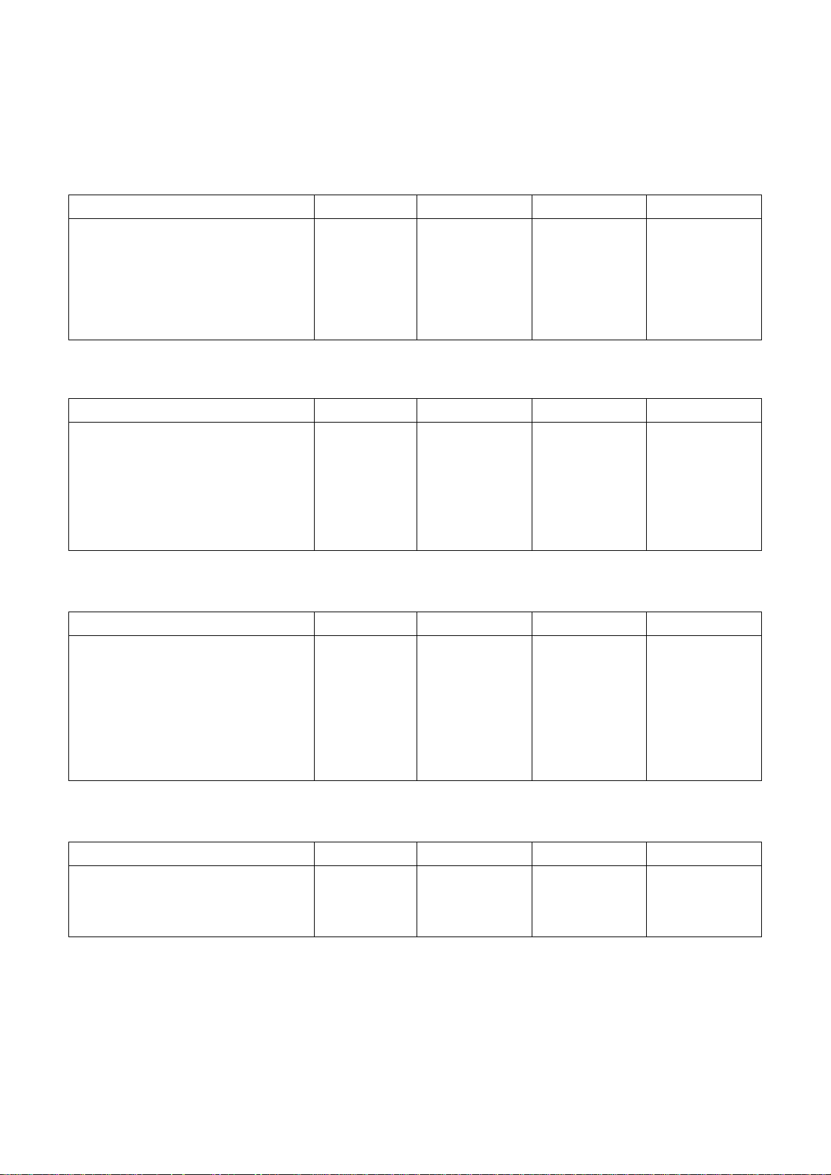
SPECIFICATIONS
<TUNER> ANT. Input ------------------- 75ohm Unbal., F type
Reference Level ----------- 20Vp-p (CRT Green Cathode)
Test Input Signal ---------- 400Hz 30% modulation
Description Condition Unit Nominal Limit
1. Intermediate Freq. Picture
Sound
MHz
MHz
45.75
41.25
-
-
2. Peak Picture Sens VHF
CATV
UHF
3. AFT Pull In Range (10mV input)
-
<DEFLECTION>
Description Condition Unit Nominal Limit
1. Deflection Freq. Horizontal
Vertical
2. Linearity Horizontal
Vertical
3. Over Scan
4. High Voltage
-
-
<VIDEO & CHROMA>
Description Condition Unit Nominal Limit
1. Misconvergence Center
Side
Corner
dBµv
dBµv
dBµv
MHz ±2.0 ±0.7
KHz
Hz
%
%
%10
KV 29
mm
mm
mm
15
15
15
15.734
60
-
-
-
-
-
30
30
40
-
-
±15
±10
-
-
0.4
1.5
2.1
2. Brightness APL 100% Ft-L 25 15
3. Color Temperature
4. Resolution Horizontal
<AUDIO>
Description Condition Unit Nominal Limit
1. Audio Output Power 10% THD W 1 0.8
2. Audio Distortion (w/LPF) 500mW % 2 7
3. Audio Freq. Response -3dB Hz 70~11K
Note:
Nominal specifications represent the design specifications. All units should be able to approximate
these. Some will exceed and some may drop slightly below these specifications. Limit specifications
represent the absolute worst condition that still might be considered acceptable. In no case should
a unit fail to meet limit specifications.
All items are measured across 8Ω load at speaker output terminal.
-
Vertical
1-1 L6200SP
°K 9200°K
Line
Line
250
300
-
-
-
-
Page 4
IMPORTANT SAFETY PRECAUTIONS
Prior to shipment from the fact ory, our products are stri ctly insp ected for reco gnize d product sa fety and el ectric al
codes of the countries in which they are to be sold. Howev er, in order to ma intain such c ompliance, it is equally
important to implement the following precautions when a set is being serviced.
Safety Precautions for TV Circuit
1. Before returning an instrument to the custom-
er, alwa ys make a saf ety check of the entire instru-
ment, including, but not limited to, the following
items:
a. Be sure that no built-in protective devices are de-
fective and have been defeated during servicing.
(1) Protective shields ar e p rovided o n this ch ass i s
to protect both the technician and the customer.
Correctly replace all missing protective shields, including any removed for servicing convenience.
(2) When reinstalli ng the cha ssis and/o r other assembly in the cabinet, be sure to put back in place
all protective devices, including but not lim ited to,
nonmetallic control knobs, insulating fishpapers,
adjustment and com part ment covers/shields, and
isolation resistor/capacitor networks. Do not oper-
ate this instrument or permit it to be operated
without all protective devices correctly installed and functioning. Servicers who defeat
safety features or fail to perform safety checks
may be liable for any resulting damage.
b. Be sure that there are no cabinet openings through
which an adult or child might be able to insert their
fingers and contact a hazardous voltage. Such
openings include, but are not l imited to, (1) spacing between the picture tube and the cabinet
mask, (2) excessively wide cabinet ventilation
slots, and (3) an improperly fitted and/or incorrectly
secured cabinet back cover.
c. Antenna Cold Check - With the instrument AC
plug removed from any AC source, connect an
electrical jumper acr oss the two AC plug prongs.
Place the instrumen t AC sw i tch in the o n position.
Connect one lead of an oh mmeter to the A C plug
prongs tied together and to uch the other ohmme ter lead in turn to each tuner antenna input exposed terminal screw and, if applicable, to the
coaxial connector. If the measured resistance is
less than 1.0 mego hm or greater than 5.2 m egohm, an abnormality exists that must be corrected
before the instrument is r eturned to th e custo mer.
Repeat this test with the ins trument AC switch in
the off position.
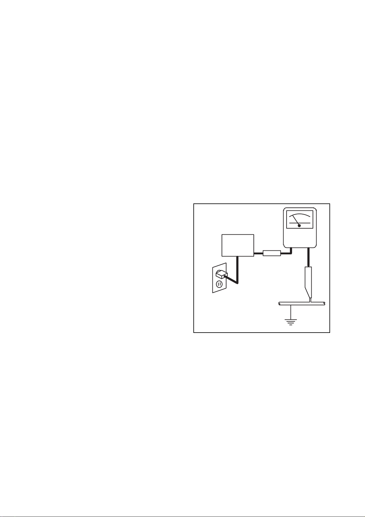
d. Leakage Current Hot Check - With the instru-
ment completely reassembled, plug the AC line
cord directly into a 120V AC outlet. (Do not use an
isolation transformer d uring this test.) Use a leak-
age current tester or a me tering sy stem tha t complies with American National Standards Institute
(ANSI) C101.1 Leakage Current for Appliances
and Underwriters Labor atories (UL) 1410, (50.7 ).
With the instrument AC switc h first in the on posi tion and then in the o ff position, measure from a
known earth ground (metal water pipe, conduit,
etc.) to all exposed metal parts of the ins trument
(antennas, handle br ackets, metal cabi net, screw
heads, metallic overlay s, control shafts, etc.) , especially any exposed metal parts that offer an electrical return path to the chassis. Any current
measured must not excee d 0.5 milli-ampere. Re verse the instrument power cord plug in t he outlet
and repeat the test.
READING SHOULD
NOT BE ABOVE 0.5 mA
LEAKAGE
DEVICE
BEING
TESTED
TEST ALL EXPOSED
METAL SURFACES
ALSO TEST WITH
PLUG REVERSED
USING AC
ADAPTER PLUG
AS REQUIRED
ANY MEASUREMENTS NO T WITHIN THE LIMI TS
SPECIFIED HEREIN INDICATE A POTENTIAL
SHOCK HAZARD THAT MUST BE ELIMINATED
BEFORE RETURNING THE INSTRUMENT TO
THE CUSTOMER OR BEFORE CONNECTING
THE ANTENNA OR ACCESSORIES.
e. X-Radiation and High Voltage Limits - Because
the picture tube is the pri mary potent ial source of
X-radiatio n in soli d-state TV receiver s, it is s pecially constructed to prohibit X-radiation emissions.
For continued X-radiation pr otection, the replacement picture tube must be the same type as the
original. Also, because the picture tube shields
and mounting hardware perform an X-radiation
protection function, they must be correctly in place.
High voltage must be mea su re d ea ch tim e s er v ic-
CURRENT
TESTER
+
EARTH
GROUND
_
2-1 L6115IMP
Page 5

ing is performed that invol ves B+, horizontal de-
flection or high voltage. Correct operation of the Xradiation protection circuits also must be reconfirmed each time they are serviced. (X-radiation
protection circuits also may be called "horiz ontal
disable" or "hold down." ) R ead a nd a ppl y th e hi gh
voltage limits a nd, if the chassis is so e quipped,
the X-radiation protection circuit specifications given on instrument labe ls and i n the P roduct S afety
& X-Radiation Warning note on the service data
chassis schematic. High voltage is maintained
within specified limits by close tolerance safety-related components/adjus tme nts in th e hig h-vo lta ge
circuit. If high voltage exceeds specified limits,
check each component specified on the chassis
schematic and take corrective action.
2. Read and comply with all caution and safety-related notes on or inside th e receiver cabine t, on the
receiver chassis, or on the picture tube.
3. Design Alteration Warning - Do not alter or add
to the mechanical or electrical design of this TV receiver. Design alterations and additions, including,
but not limited to circuit modificatio ns and the addition of items such as auxiliary audio and/or video
output connections, mig ht alter the saf ety char acteristics of this receiver and create a hazard to the
user. Any design alter ations or addition s will void
the manufacturer's warr anty and may make you,
the servicer, responsible for personal injury or
property damage resulting therefrom.
4. Picture Tube Implosion Protection Warning -
The picture tube in this receiver employs integral
implosion protection. For continued implosion protection, replace the pic ture tube only with one of
the same type numbe r. Do not rem ove, install , or
otherwise handle the picture tube in any ma nner
without first putting on shatterproof goggles
equipped with side shields. People not so
equipped must be ke pt safely away while p icture
tubes are handled. Keep the picture tube away
from your body. Do not handl e the pictur e tu be b y
its neck. Some "in-line" picture tubes are equipped
with a permanently at tached deflection yoke; be cause of potential hazard, do not try to remove
such "permanently attac hed" yokes from the picture tube.
5. Hot Chassis Warning -
a. Some TV receiver chassis are electrically connect-
ed directly to one conduc tor of the AC power cord
and maybe safety-serviced without an isolation
transformer only i f the AC power plug i s inserted
so that the chassis is connected to the ground side
of the AC power source. To confi rm that the AC
power plug is ins erted correctly, with an AC voltmeter, measure between the chassis and a known
earth ground. If a voltage reading in excess of 1.0V
is obtained, remove and reinsert the AC power
plug in the opposite polarity and again measure
the voltage potential between the chassis and a
known earth ground.
b. Some TV receiver chassis normally have 85V
AC(RMS) between ch assis and earth ground regardless of the AC plug polarity. This chassis can
be safety-serviced only with an isolation transformer inserted in the power line between the receiver
and the AC power so urce, fo r both personn el and
test equipment protection.
c. Some TV receiver chassis have a secondary
ground system in addition to the main chassis
ground. This se conda ry gro und s ystem is no t iso lated from the AC power line. The two ground systems are electrically separated by insulation
material that must not be defeated or altered.
6. Observe original lead dress. Take extra care to assure correct lead dress in the following areas:a.
near sharp edges,b. near thermally hot parts-be
sure that leads and components do not touch thermally hot parts, c. the AC supply,d. high voltage,
and,e. antenna wir ing. Al ways in sp ect in a ll are as
for pinched, out of pl ace, or frayed wiring. C heck
AC power cord for damage.
7. Components, parts, and/or wiring that appear to
have overheated or are otherwise damaged
should be replaced with components, parts, or wiring that meet origin al specifications. Additiona lly,
determine the cause of ov erheating and/or damage and, if nece ss ar y, ta ke co rre cti ve ac ti on t o remove any potential safety hazard.
8. Product Safety Notice - Some electrical and mechanical parts have s pecia l safety- relat ed char acteristics which are often not evident from visual
inspection, nor can the protection they give necessarily be obtained by replaci ng them with components rated for higher voltage, wattage, etc.. Parts
that have special safety characteristics are identified by a ( # ) on schematics and in parts lists. Use
of a substitute replacement that does not have the
same safety characteristics as the recommended
replacement part might create sh ock, fire, and/or
other hazards. The product's safety is under review continuously and new instructions are issued
whenever appropriate . Prior to shi pment from the
factory, our products are strictly inspected to confirm they comply with the recognized product safety and electrical codes of the countries in which
they are to be sold. Howev er, in orde r to mai ntain
such compliance , it is equally important to im plement the following precautions when a set is being
serviced.
2-2 L6115IMP
Page 6

Precautions during Servicing
A. Parts identified b y the ( # ) symbo l are c ritica l for
safety.
Replace only with part number specified.
B. In addition to safety, othe r parts and assemblies
are specified for conformance with regulations applying to spurious radiati on. These must also be
replaced only with specified replacements.
Examples: RF converters, RF cables, noise blocking capacitors, and noise blocking filters, etc.
C. Use specified internal wiring. Note especially:
1) Wires covered with PVC tubing
2) Double insulated wires
3) High voltage leads
D. Use specified insulating materials for hazardous
live parts. Note especially:
1) Insulation Tape
2) PVC tubing
3) Spacers
4) Insulators for transistors.
E. When replacing AC primary side components
(transformers, power cord, etc.), wrap ends of
wires securely abo ut the terminals before so ldering.
F. Observe that the wires do not contact heat produc-
ing parts (heatsinks, oxide metal film resistors, fusible resistor s, et c .)
G. Check that replaced wires do not contact sharp
edged or pointed parts.
H. When a power cord has been replaced, check that
5~6 kg of force in any direction will not loosen it.
I. Also check areas surrounding repaired locations.
J. Use care that foreign objects (screws, solder drop-
lets, etc.) do not remain inside the set.
K. Crimp type wire connector
The power transform er uses crimp type connec-
tors which connect the power cord and the primary
side of the transformer. When replacing the trans-
former, follow these step s carefully and precis ely
to prevent shock hazards.
Replacement procedure
1) Remove the old connector by cutti ng the wires at
a point close to the connector.
Important: Do not re-use a connector (discard it).
2) Strip about 15 mm of the insulation from the end s
of the wires. If the wires are stranded, twist the
strands to avoid frayed conductors.
3) Align the lengths of the wires to be connected. Insert the wires fully into the connector.
4) Use the crimping tool to crimp the metal sleeve at
the center position . Be sure to crimp fully to the
complete closure of the tool.
L. When connecting or disconnecting the internal
connectors, first, discon nect the AC plug from the
AC supply outlet.
2-3 L6115IMP
Page 7
Safety Check after Servicing
Examine the area surrounding the repaired location
for damage or deterioration. Observe that screws,
parts and wires have been returne d to original positions. Afterwards, perform the following tests and confirm the spec ified values in order to verify compli ance
with safety standards.
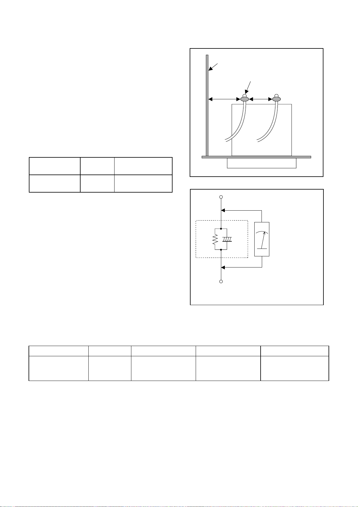
1. Clearance Distance
When replacing primary circuit components, confirm
specified clearance distance ( d) and (d') between soldered terminals, and between terminals and surrounding metallic parts. (See Fig. 1)
Table 1 : Ratings for selected area
AC Line Voltage Region
110 to 130 V
Note: This table is unofficial and for reference only. Be
sure to confirm the precise values.
USA or
CANADA
Clearance
Distance (d) (d')
≥ 3.2 mm
(0.126 inches)
2. Leakage Current Test
Confirm the specified (or lower) leakage current between B (earth ground, power cord plu g prongs) and
externally exposed accessible parts (RF terminals, antenna termina ls, video an d au dio in put and output te rminals, microphone jacks, earphone jacks, etc.) is
lower than or equal to the spe cified value in the table
below.
Measuring Method : (Power ON)
Insert load Z between B (earth ground, power cord
plug prongs) and exposed accessible parts. Use an
AC voltmeter to measure across both terminals of
load Z. See Fig. 2 and following table.
Z
1.5kΩ
Chassis or Secondary Conductor
Primary Circuit Terminals
dd'
Exposed Accessible Part
AC Voltmeter
0.15µF
Earth Ground
B
Power Cord Plug Prongs
(High Impedance)
Fig. 1
Fig. 2
Table 2 : Leakage current ratings for selected areas
AC Line Voltage Region Load Z Leakage Current (i) Earth Ground (B) to:
0.15µF CAP. & 1.5kΩ
110 to 130 V USA
Note: This table is unofficial and for reference only. Be sure to confirm the precise values.
RES. connected in
parallel
2-4 L6115IMP
i≤0.5mA rms
Exposed accessible
parts
Page 8
STANDARD NOTES FOR SERVICING
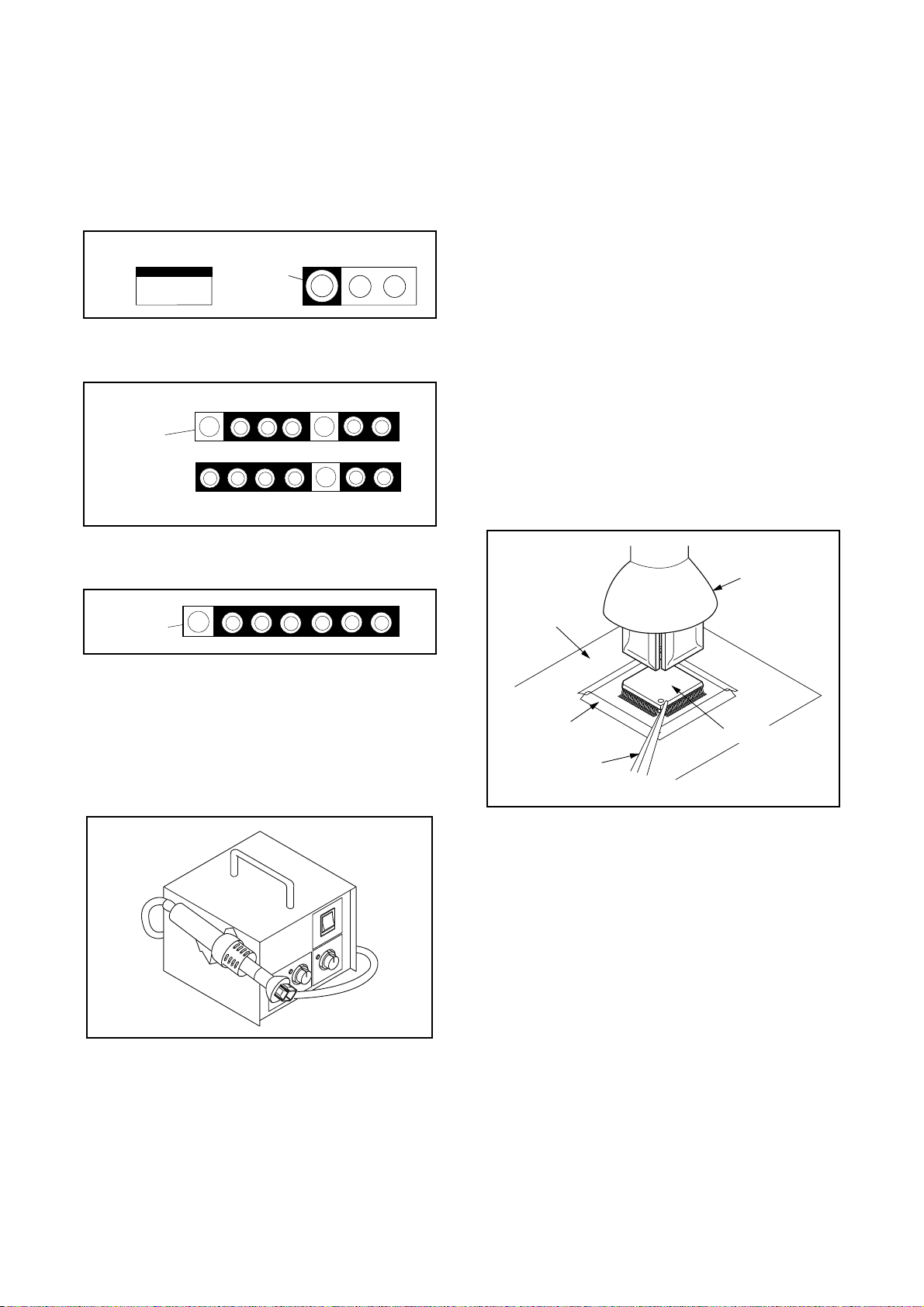
Circuit Board Indications
a. The output pin of the 3 pin Regulator ICs is indicat-
ed as shown.
Top View
Out
b. For other IC s, pin 1 a nd ev er y fifth pin ar e in dic at -
ed as shown.
Pin 1
c. The 1st pin of every male connector is indicated as
shown.
Pin 1
Input
In
Bottom View
5
10
(2) Remove the flat pack-IC with tweez ers while ap-
plying the hot air.
(3) Bottom of the flat pack -IC is fix ed with glu e to the
CBA; when removing entire flat pack-IC, first apply
soldering iron to center of the flat pack-IC and heat
up. Then remove (glue will be melted). (Fig. S-1-6)
(4) Release the flat pack-IC from the CBA using twee-
zers. (Fig. S-1-6)
Caution:
1. Do no t supply hot air to the ch ip parts aroun d the
flat pack-IC for over 6 seconds because damage
to the chip parts may occur. Put masking tape
around the flat pack-IC to protec t other par ts from
damage. (Fig. S-1-2)
2. The flat pack-IC on the CBA is affixed with glue, so
be careful not to br eak or d amage the foi l of ea ch
pin or the solder lands u nder the IC when rem oving it.
Hot-air
Flat Pack-IC
Desoldering
Machine
CBA
How to Remove / Install Flat Pack-IC
1. Removal
With Hot-Air Flat Pack-IC Desoldering Machine:
(1) Prepare the hot-air flat pack-IC desoldering ma-
chine, then apply hot air to the Flat Pack-IC (about
5 to 6 seconds). (Fig. S-1-1)
Fig. S-1-1
Masking
Tape
Tweezers
Flat Pack-IC
Fig. S-1-2
3-1 L6115STA
Page 9
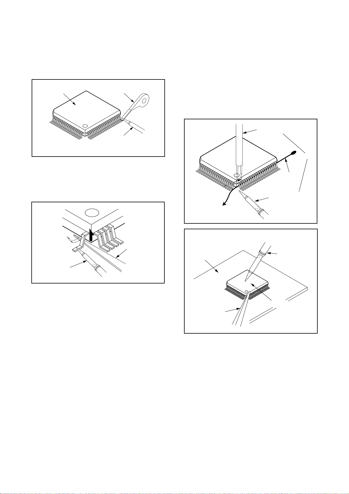
With Soldering Iron:
(1) Using desolderin g braid, remove the solder from
all pins of the flat pac k-IC. When you use solde r
flux which is appl ied to all pins of the flat pa ck- IC,
you can remove it easily. (Fig. S-1-3)
Flat Pack-IC
Desoldering Braid
Soldering Iron
Fig. S-1-3
(2) Lift each lead of the flat pac k-IC upward one by
one, using a sharp pin or wire to which solder will
not adhere (iron wire). When heating the pins, use
a fine tip soldering iron or a hot air desoldering machine.(Fig. S-1-4)
soldering iron to center of the flat pack-IC and heat
up. Then remove (glue will be melted). (Fig. S-1-6)
(5) Release the flat pack-IC from the CBA using twee-
zers. (Fig. S-1-6)
Note:
When using a soldering iron, care must be taken to
ensure that the flat pack -IC is not being held by
glue. When the flat pack-IC is removed from the
CBA, handle it gently because it may be damaged
if force is applied.
Hot Air Blower
or
Iron Wire
Soldering Iron
To Solid
Mounting Point
Fig. S-1-5
Sharp
Pin
Fine Tip
Soldering Iron
Fig. S-1-4
(3) Bottom of the flat pack-IC is fi xed with g lue to the
CBA; when removing entire flat pack-IC, first apply
soldering iron to center of the flat pack-IC and heat
up. Then remove (glue will be melted). (Fig. S-1-6)
(4) Release the flat pack-IC from the CBA using twee-
zers. (Fig. S-1-6)
With Iron Wire:
(1) Using desolderin g braid, remove the solder from
all pins of the flat pac k-IC. When you use solde r
flux which is appl ied to all pins of the flat pa ck- IC,
you can remove it easily. (Fig. S-1-3)
(2) Affix the wire to a workbench or solid mounting
point, as shown in Fig. S-1-5.
(3) While heating the pins using a fine tip soldering
iron or hot air blower, pull up the wire as the solder
melts so as to lift the IC leads from the CBA contact pads as shown in Fig. S-1-5.
(4) Bottom of the flat pack-IC is fi xed with g lue to the
CBA; when removing entire flat pack-IC, first apply
CBA
Tweezers
Fine Tip
Soldering Iron
Flat Pack-IC
Fig. S-1-6
3-2 L6115STA
Page 10
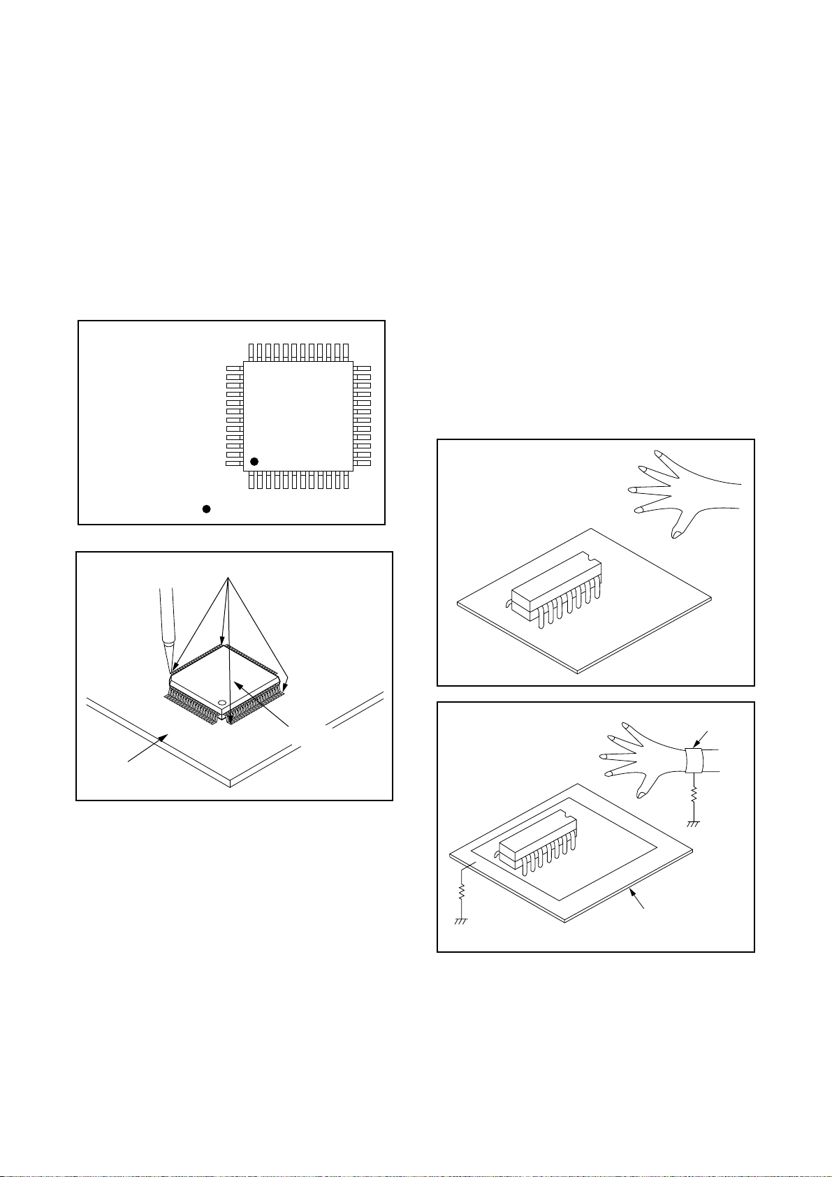
2. Installation
(1) Using desolderin g braid, remove the solder from
the foil of each pin of the flat pac k-IC on the CBA
so you can install a replacement flat pack-IC more
easily.
(2) The "I" mark on the flat pack-IC indi cates pin 1.
(See Fig. S-1-7.) Be sure this mark matches the 1
on the PCB when positioning for installation. Then
pre- solder the four corners of the flat pack-IC.
(See Fig. S-1-8.)
(3) Solder all pins of the flat pack-IC. Be sure that
none of the pins have solder bridges.
Example :
Pin 1 of the Flat Pack-IC
is indicated by a " " mark.
Fig. S-1-7
Instructions for Handling
Semiconductors
Electrostatic breakdown of the semiconductors may
occur due to a potential difference c aused by electrostatic charge during unpacking or repair work.
1. Ground for Human Body
Be sure to wear a grounding band (1MΩ) tha t is properly grounded to rem ove any static electr ic i ty th at may
be charged on the body.
2. Ground for Workbench
Be sure to place a conducti ve shee t o r copper plate
with proper grounding (1MΩ) on the workbench or
other surface, where the semiconductors are to be
placed. Because the static electr icity charge on clothing will not escape through the body grounding band,
be careful to avoid contacting semiconductors with
your clothing.
<Incorrect>
CBA
Presolder
Flat Pack-IC
Fig. S-1-8
<Correct>
1MΩ
CBA
Grounding Band
1MΩ
CBA
Conductive Sheet or
Copper Plate
3-3 L6115STA
Page 11
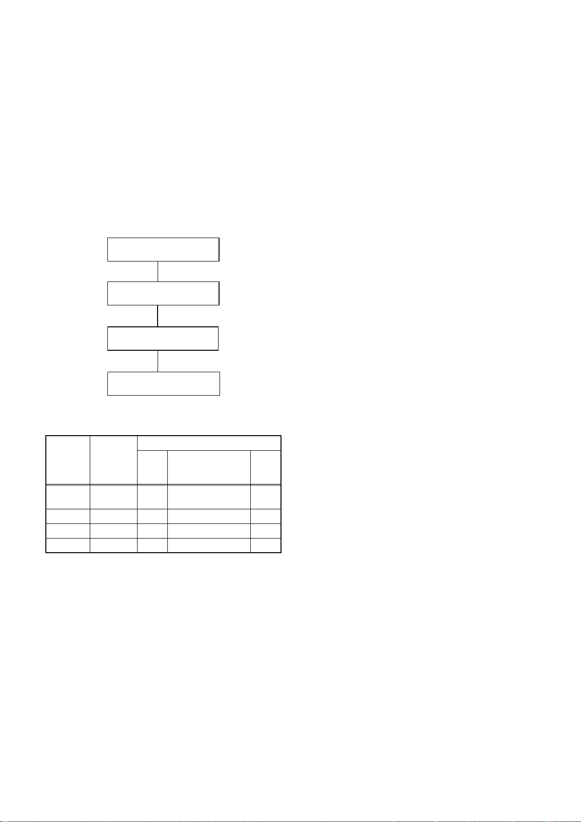
CABINET DISASSEMBLY INSTRUCTIONS
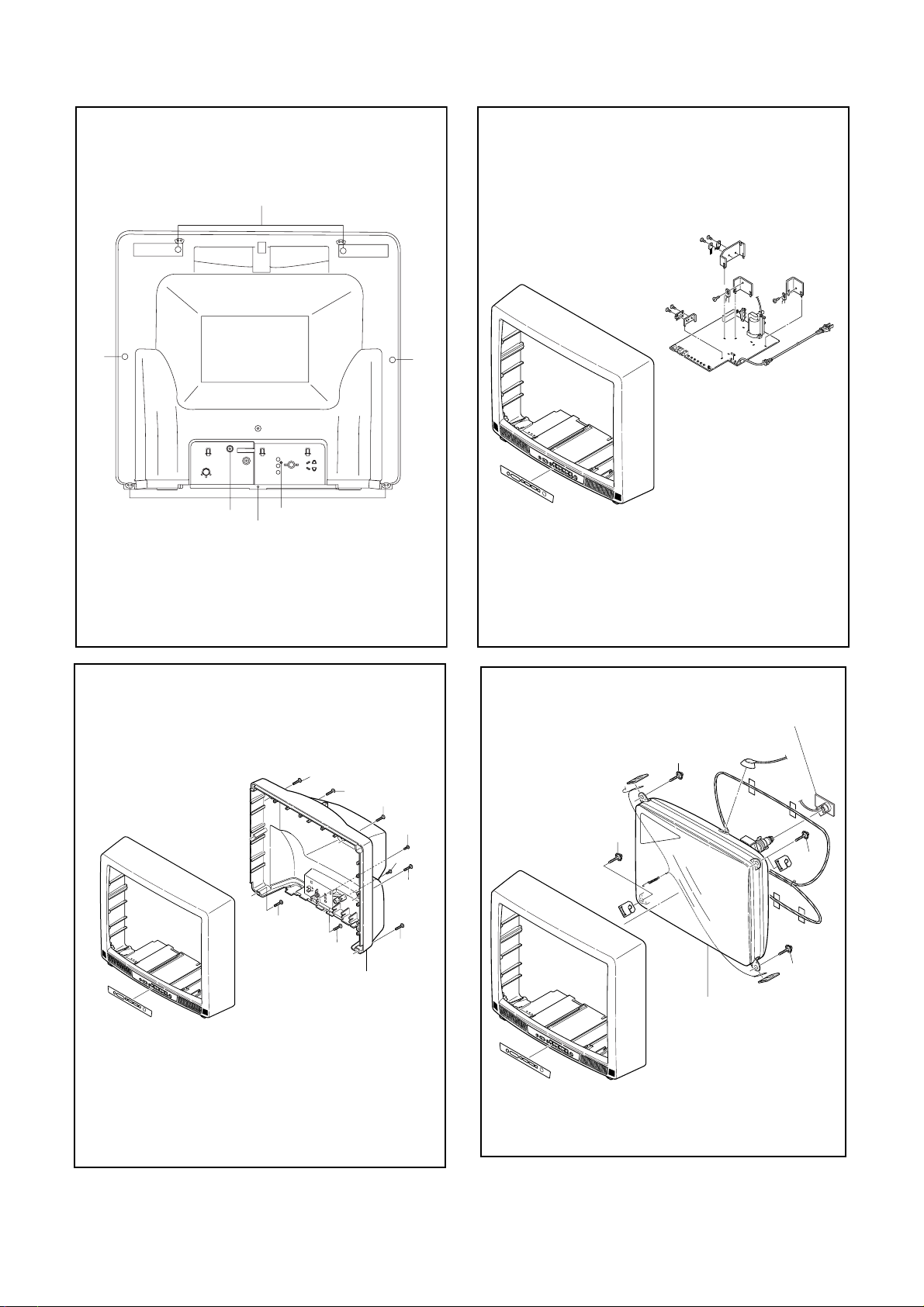
1. Disassembly Flowchart
This flowchart indicates the disassembly steps for the
cabinet par ts, and the CBA in order to gain ac cess to
item(s) to be se r vic ed. W hen reass embling, follow the
steps in reverse order. Bend, route and dress the
cables as they were.
Caution !
When removing the CRT, be sure to discharge the
Anode Lead of the CRT with the CRT Ground Wire
before removing the Anode Cap.
[1] Rear Cabinet
[2] CRT CBA
[3] Main CBA
[4] CRT
2. Disassembly Method
Removal
Step/
Loc. No.
[1]
[2] CRT CBA 4,5 CN501 2
[3] Main CBA 3,5 CN571 3
[4] CR T 4 4(S-3), Anode Cap 4
Part
Rear
Cabinet
Fig.
No
1,2
Remove/*unlock/
release/unplug/
unclamp/desolder
7(S-1), 1(S-2),
1(S-4)
Note
1
Note :
(1) Order of steps in procedu re. When reas sembling,
follow the steps in reverse order.These number s
are also used as the Identification (location) No. of
parts in figures.
(2) Parts to be removed or installed.
(3) Fig. No. showing procedure of part location
(4) Identification of part to be removed, unhooked, un-
locked, released, unplugged, unclamped, o r desoldered.
S=Screw, P=Spring, L=Locking Tab, CN=Connector, *=Unhook, Unlock, Release, Unplug, or
Desolder
2(S-2) = two Screws (S-2)
(5) Refer to the following "Reference Notes in the
Table."
Reference Notes in the Table
1. Removal of the Rear Cabinet. Remove screws
7(S-1), 1(S-2) and 1(S-4) then slide the Rear Cabinet backward.
2. Removal of the CRT CBA. Disconnect CN501 then
pull the CRT CBA backward.
3. Removal of the Main CB A. Disconne ct CN571 on
the Main CBA then slide the Main CBA backward.
Caution:
Discharge the Anode Lead o f the CRT with the CRT
Ground Wire before removing the Anode Cap.
4. Removal of the CR T. Remo ve sc rews 4(S- 3) and
Anode Cap. then slide the CRT backward.
↓↓↓↓↓
(1) (2) (3) (4) (5)
4-1 L6601DC
Page 12
S-1
S-1
S-4
S-1
S-2
[1] Rear Cabinet
S-1
S-1
Fig. 1
S-1
S-1
S-3
Anode Cap
[3] Main CBA
Fig. 3
[2] CRT CBA
S-1
S-1
[1] Rear Cabinet
S-2
S-4
S-1
S-1
Fig. 2
S-3
S-3
S-3
[4] CRT
Fig. 4
4-2 L6601DC
Page 13
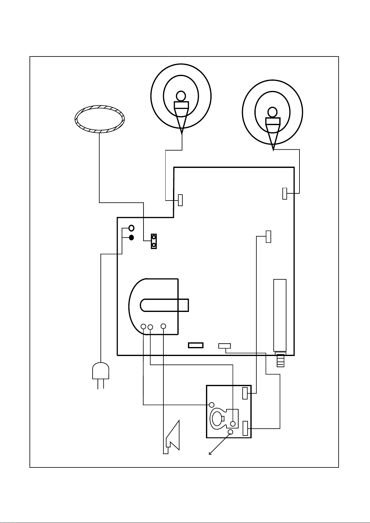
TV Cable Wiring Diagram
SP802
SP801
DG691 DEGAUSSING COIL
MAIN CBA
CN691
FLYBACK TRANSFORMER
T571
CLN802
CLN801
CN801
CN802
WH301A
TU1
TUNER
AC601
AC CORD
CN571
FOCUS
SCREEN
ANODE
WH501A
JK1501
CN1501
TO CRT GROUND
WH301B
WH501B
Fig. 5
4-3 L6601DC
Page 14
ELECTRICAL ADJUSTMENT INSTRUCTIONS
General No te :
"CBA" is abbreviation for "Circuit Board Assembly".
NOTE:
Electrical adjustm ent s ar e r equ ired after replacing
circuit components a nd certain mechanic al parts.
It is important to perform these adjustm ents only
after all repairs and replacements have been completed.
Also, do not attempt these adjustments unless the
proper equipment is available.
Test Equipment Required
1. NTSC Pattern Generator (Color Bar W/White
Window, Red Color, Dot Pattern, Gray Scale,
Monoscope, Multi-Burst)
2. DC Voltmeter
3. Oscilloscope: Dual-trace with 10:1 probe,
V-Range:0.001~50V/Div,
F-Range:DC~AC-60MHz
4. Plastic Tip Driver
5. Remote control unit:Part No. N0127UD or N0132UD
or N0105UD or N 01 08UD
6. DC power supply 13.2V/5A
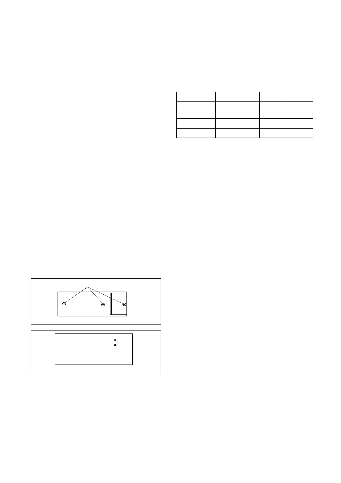
How to make Service rem ote control unit:
1.
Prepare normal remote control unit. (Part No.
N0127UD or N0132UD or N0105UD or N0108UD)
Remove 3 Screws from the back lid. (Fig. 1-1)
2 . Add J1 (Jumper Wire) to the remote control CBA.
(Fig. 1-2)
SCREWS
REMOTE CONTROL UNIT
Fig. 1-1
1. DC 120V Adjustment
Purpose: To obtain correct operation.
Symptom of Misadjustment: The picture is dark and
the unit does not operate correctly.
Test Point Adj. Point Mode Input
TP601(+120)
TP300(GND)
Tape M. EQ. Spec.
--- DC Voltmeter +120±0.5V DC.
Note:TP601, TP300(GND), VR661 --- Main CBA
1. Connect DC Volt M ete r t o TP6 01 an d TP300 (GN D).
2. Adjust VR661 so th at the voltage o f TP60 1 becomes
+120±0.5V DC.
VR661 --- ---
2. Black Strech Control Adjustment
Purpose: To show the fine black color.
Symptom of Misadjustment: Black color will not
appear correctly.
Note: Use Service remote control unit.
1. Enter the Service mode. (See page 5-1)
2. P ress " 6 " button on the Servic e remote control
unit. " B-S " is indicated.
3. Press " CH o / p " buttons on the Service remote
control unit so that display will change " OFF ", " 0
", " 1 ", " 2 " and " 3 ". Then choose " B-S OFF ".
4. P ress " 6 " button on the Servic e remote control
unit. " B-S*2 " is indicated.
5. Press " CH o / p " buttons on the Service remote
control unit so tha t display will change " 0 " and
" 1 ". Then choose " B-S*2 0".
6. Turn the power off and on again. (Main power button on the TV unit.)
J 1
REMOTE CONTROL CBA
Fig. 1-2
5-1 L6605EA
Page 15

3-1. Setting for 7F and FRENCH
data Values
General
1. Enter the Service mode. (See page 5-1)
2. Press " VOL p " button on the Service remote control uni t. Dis pla y c han ges " C /D ", " 7 F " , "FRENCH
", " ACCESS CODE ", " STEREO ", " VIDEO TONE
", " FM-MO DE ", a nd " V- OUT " cyclically when "
VOL p " button is pressed.
7F
1. Press " VOL p " button on the Service remote control unit. Then select 7F display.
2. Press " CH o / p " buttons on the Service remote
control unit. Then choose 7F=FF.
FRENCH
1. Press " VOL p " button on the Service remote control unit. Then select FRENCH display.
2. Press " CH o / p " buttons on the Service remote
control unit. Then choose FRENCH=ON.
TINT (TNT)
1. Press " MENU " butto n on th e Ser vice r emote control unit. Then select " TINT " (TNT) display.
2. Press " CH o / p " buttons on the Service remote
control unit so that the value of " TINT " (TNT) becomes 62.
V-TINT (V-TNT)
1. Press " ME NU " but ton on the S ervi ce remo te control unit. Then select " V-TINT " (V-TNT) display.
2. Press " CH o / p " buttons on the Service remote
control unit so that the value of " V-TINT " (V-TNT)
becomes 59.
SHARP (SHARP)
1. Press " MENU " butto n on th e Ser vice r emote control unit. Then select " SHARP " (SHARP) display.
2. Press " CH o / p " buttons on the Service remote
control unit so that the value of “ SHARP "
(SHARP) becomes 47.
Note: BRIGHT data value does not need to be adjust-
ed at this moment.
ACCESS CODE ---- set to OFF
VIDEO TONE ---- set to ON
FM-MODE ---- set to OFF
V-OUT ---- set to OFF
STEREO ---- set to ON
Note: C/D and VCO data values do not need to be
adjusted at this moment.
3-2. Setting for CONTRAST,
COLOR, TINT, V-TINT and
SHARP data Values
General
1. Enter the Service mode. (See page 5-1)
2. Press " MENU " button on the Service remote control
unit. Display changes " BRIGHT ", " CONTRAST ",
" COLOR ", " TINT ", " V-TINT " and " SHARP "
cyclically when " MENU " button is presse d.
CONTRAST (CNT)
1. Press " MENU " button on the Se rvi c e rem o t e co ntrol unit. Then select " CONTRAST " (CNT) display.
2. Press " CH o / p " buttons on the Service remote
control unit so that the value of " CONTRAST "
(CNT) becomes 84.
COLOR (CLR)
1. Press " MENU " button on the Service remote control unit. Then select " COLOR " (CLR) display.
2. Press " CH o / p " buttons on the Service remote
control unit so tha t the valu e of " COLO R " (CLR )
becomes 58.
4. Black Level Adjustment
Purpose: Set Black Level
Symptom of Misadjustment: If black level is incor-
rect, Proper br ig htn ess c an not be o bta ine d by adj usting the Brightness Control .
1. Enter the Service mode. (See page 5-1).
2. Press " MENU " butto n on th e Ser vice r emote control unit and select " BRT "mode. (Display changes
" BRT ", " CNT ", " CLR ", and " TNT " cyclically
when MENU button is pressed).
3. Press " CH o / p " buttons on the Service remote
control unit so that the value of " B RT " becomes
128.
4. Turn the power off and on again. (Main power button on the TV unit.)
5-2 L6605EA
Page 16
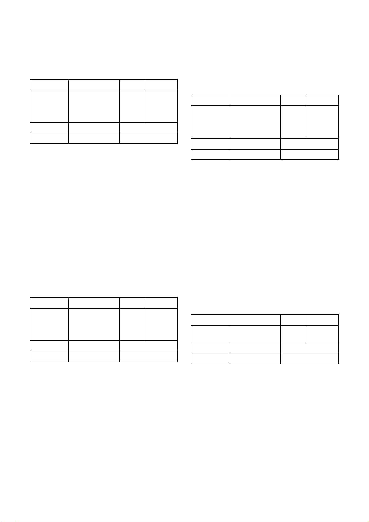
5. V. Size Adjustment
Purpose: To obtain correct vertical width of screen image.
Symptom of Misadjustment: If V. Size is incorrect, vertical
size of image on the screen may not be properly displayed.
Test Point Adj. Point Mode Input
Screen Cont rol
---
Tape M. EQ. Spec.
--- Monoscope 90±5%
Note: Use service remote control unit.
1. Operate the unit for at least 20 minutes.
2. Enter the Service mode. (See page 5-1)
3. Receive the Monoscope Pattern.
4. Press " 9 " button on the Service remote control unit
and select " V- S " mode. (Di splay cha nges " V-S "
and " V-P " cyclically when " 9 " button is pressed).
5. Press " CH o / p " buttons on the Service remote
control unit so that the m onoscope pattern will be
90±5% of display size and the circle is round.
6. Turn the power off and on again. (Main power button on the TV unit.)
CH o / p
buttons [ V -S ]
Mode
RF
Mono-
scope
6. V. Position Adjustment
Purpose: To obtain correct vertical width of screen
image.
Symptom of misadjustment: If V. Position is incor-
rect, vertical height of image on the screen may not be
properly displayed.
Test Point Adj. Point Mode Input
Screen Cont rol
---
Tape M. EQ. Spec.
--- Monoscope 90±5%
CH o / p
buttons [ V -P ]
Mode
RF
Mono-
scope
7. H. Position Adjustment
Purpose: To obtain correct horizontal position of
screen image.
Symptom of Misadjustment: If H. Position is incor-
rect, horizontal po sition of image on the screen may
not be properly displayed.
Test Point Adj. Point Mode Input
Screen Control
---
Tape M. EQ. Spec.
--- Monoscope 90±5%
Note: Use Service remote control unit
1. Operate the unit for at least 20 minutes.
2. Enter the Service mode. (See page 5-1)
3. Receive the Monoscope Pattern.
4. Press " 8 " button on the remote control uni t and
select " H-P "mode.
5. Press " CH o / p " buttons on the Service remote
control unit so th at the mono scope patte rn will be
90±5% of display size and the circle is round.
6. Turn the Power off and on again. (Main power button on the TV unit.)
CH o / p
buttons [ H-P ]
Mode
RF
Mono-
scope
8. H. Size Adjustment
Purpose: To obtain correct horizontal size of screen
image.
Symptom of Misadjustment: If H. Size is incorrect,
horizontal size of image on the screen may not be
properly displayed.
Test Point Adj. Point Mode Input
--- VR562 RF
Tape M. EQ. Spec.
--- Monoscope 90±5%
Mono-
scope
Note: Use Service remote control unit
1. Operate the unit for at least 20 minutes.
2. Enter the Service Mode. (See page 5-1)
3. Receive the Monoscope Pattern.
4. Press " 9 " button on the Service remote control unit
and select " V-P "mode. (Display change " V-S " and
" V-P " cyclically when " 9 " button is pressed).
5. Press " CH o / p " buttons on the Service remote
control unit so that the top and bottom of the monoscope pattern will be equal of each other.
6. Turn the Power off and on again. (Main power button on the TV unit.)
Note: Use Service remote control unit
1. Operate the unit for at least 20 minutes.
2. Receive the Monoscope Pattern.
3. Adjust V R562 so that the monoscop e pattern will
4. Turn the Power off and on again. (Main power but-
5-3 L6605EA
be 90±5% of display size and circle is round.
ton on the TV unit.)
Page 17
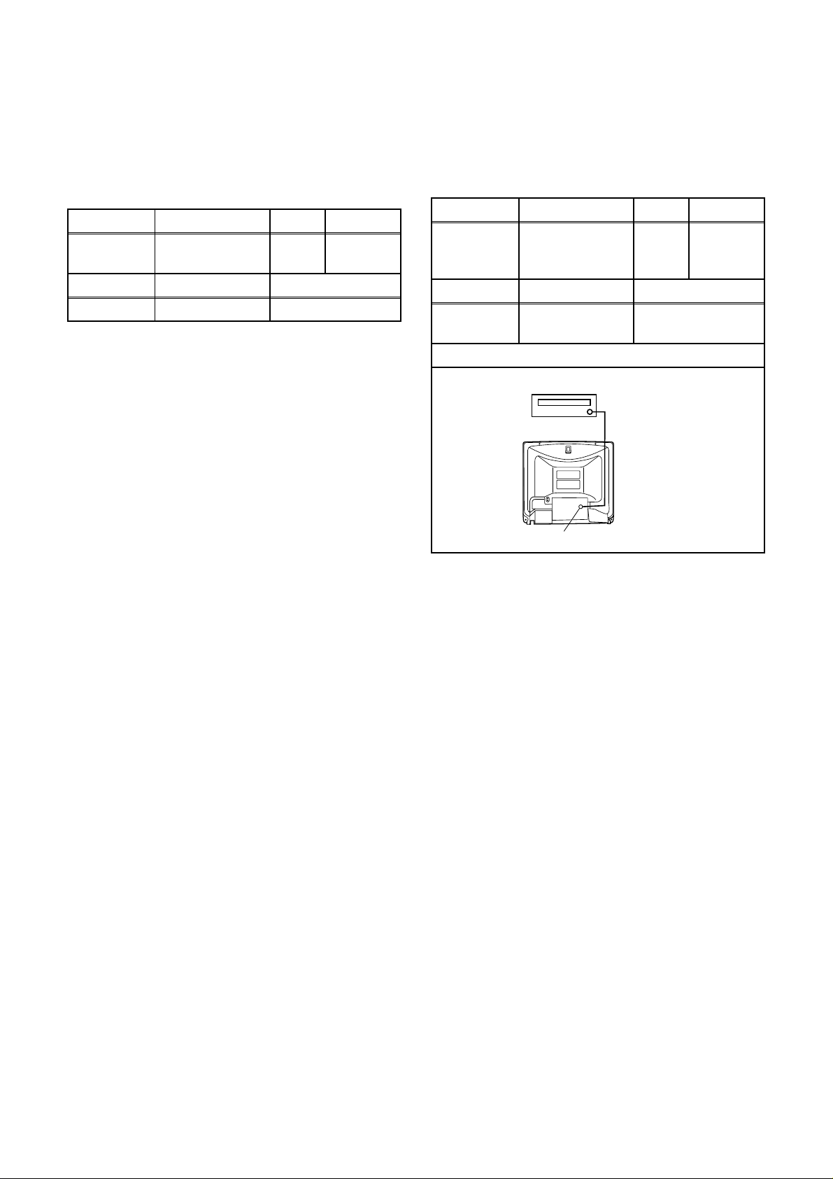
9. PIN Cushion Adjustment
Purpose: To obtain correct straight vertical line of
screen image.
Symptom of Misadjustment: If H.Pin cushion is incorrect, vertical line of image on the sc reen may not be
properly displayed.
Test Point Adj. Point Mode Input
--- VR561 RF
Tape M. EQ. Spec.
--- Cross hatch
Note: Use Service remote control unit
1. Operate the unit for at least 20 minutes.
2. Receive the Cro ss hatch Pattern.
3. Adjus t VR561 so that the cross hatc h pattern will
be straight line of display.
4. Turn the Power off and on again. (Main power button on the TV unit.)
Cross
hatch
10. Cut-off Adjustment
Purpose: To adjust the beam cur rent of R, G, B, and
screen voltage.
Symptom of Misadjustment: White color may be
reddish, greenish or bluish.
Test Point Adj. Point Mode Input
Screen-Control
---
Tape M. EQ. Spec.
---
CH o / p
buttons
Pattern
Generator
Figure
PATTERN GENERATOR
RF
See Reference
Notes below.
Black
Raster
EXT. INPUT
Note: Screen Control FBT --- Main CBA
F.B.T= Fly Back Transformer
Use Service remote control unit
1. Degauss the CRT and allow CRT to operate for 20
minutes before starting the alignment.
2. Input the Black Raster Signal from RF Input.
3. Enter the Service mode. (See page 5-1)
4. Press " VOL p " butto n on the Serv ice remote co ntrol unit and select " C/D " mode. (Display changes
" C/D ", " 7F ", " FRENCH ", " ACCESS CODE ", "
STEREO ", " VIDEO TON E ", " FM -MOD E ", a nd "
V-OUT " cyclically when " VOL p " button is
pressed.) then press " 1 ". The display will momentarily show " CUT OFF R " (R= Red). Now there
should be a horizontal line across the center of the
picture tube. If needed gra dually turn the screen
control on the flyba ck, c lo ckw ise unt il the hor iz on tal line appears. Adjust the Red Cut off by pressing
the " CH o / p " buttons. Proceed to Step 5 when
the Red Cut off adjustment is done.
5 . Press the " 2 "button. The display will momentarily
show " CUT OFF G " (G=Green). Adjust the Green
Cut off by pressing the " C H o / p " buttons . Proceed
to step 6 when the Green Cut off a djustment is do ne.
6. Press the " 3 " button. The disp lay will mom entari ly
show " CUT OFF B " (B=Blue). Adjust the Blue cut
off by pressing the " CH o / p " buttons. When
done with steps 4, 5 and 6 the horizontal line
should be pure white if not, then attempt the Cut off
adjustment again.
Fig. 2
5-4 L6605EA
Page 18
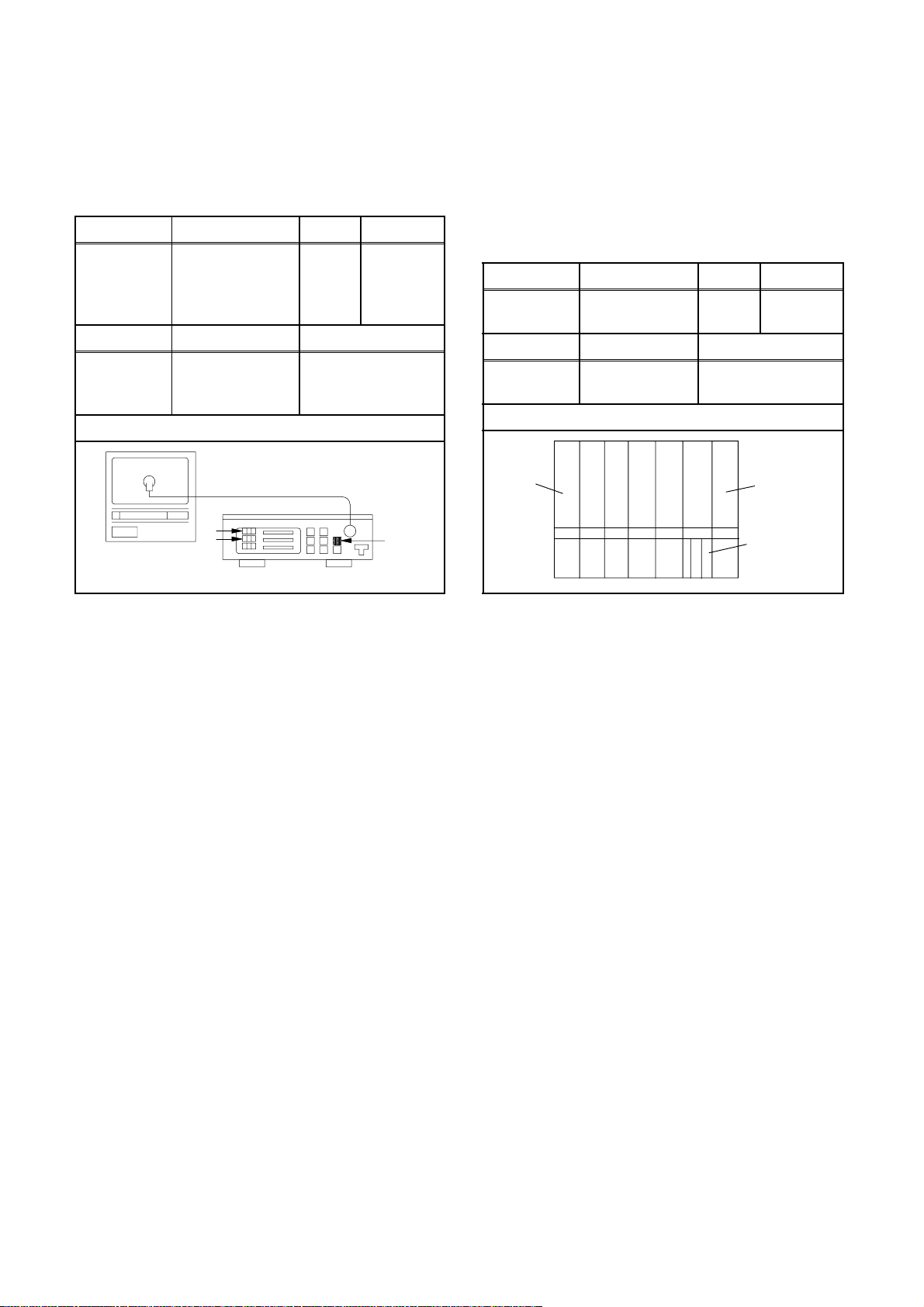
11. White Balance Adjustment
Purpose: To mix red, green and blue beams correctly
for pure white.
Symptom of Misadjustment: White becomes bluish
or reddish.
Test Point Adj. Point Mode Input
White
Screen
Tape M. EQ. Spec.
CH o / p
buttons
Pattern
Generator,
Color analyzer
Figure
RF
Raster
(APL
100%)
See below
Note: Confirm that Cut Off Adj. is correct after this
adjustment, and attemp t Cut Off Adj. if neede d.
12. Sub-Brightness Adjustment
Purpose: To get proper brightness.
Symptom of Misadjustment: If Sub-Brightness is
incorrect, proper brightness cannot be obtained by
adjusting the Brightness Control.
Test Point Adj. Point Mode Input
---
Tape M. EQ. Spec.
---
CH o / p
buttons
Pattern
Generator
Figure
RF IQW
See below
Color Analyzer
Note: Use Service remote control unit
1. Operate the unit more than 20 minutes.
2. Face the unit to east. Degauss the CRT using De gaussing Coil.
3. Input the White Raster (APL 100%).
4. Set the color analyzer to the CHROMA mode and after zero point calibration, bring the optical receptor to
the center on the tube surface (CRT).
5. Enter the Service mode. Press " VOL p " button on
the Service remote control unit and select " C/D "
mode. (Display changes " C/D ", " 7F ", " FRENCH ",
" ACCESS CODE ", " STEREO ", " VIDEO TONE
", " FM-MODE ", and " V-OUT " cyclically when "
VOL p " button is pressed.) then Press No. 8 button
on the Service remote control Unit.
6. Press No. 4 button on the service remote control unit
for Red adjustment. Press N0 . 5 button on the Ser vice remote control unit for Blue adjustment.
7. In each color mode, Press " CH o / p " button to adjust the values of color.
8. Adjusting Red and Blue color so that the temperature
becomes 9200K (x : 286 / y : 294)±3%.
9. At this time, Re-check that Horizo ntal line is white. If
not, Re-adjust Cut-off Adjustment until the Horizontal
Line bec omes pu re w hi te.
10. Turn off and on again to retur n to no rm al mod e. Re ceive APL 100% white signal and Check Chroma
temperatures become 9200K (x : 286 / y : 294)±3%.
Fig. 3
White
Note: IQW Setup level --- 7.5 IRE
Use Service remote control unit
1. Enter the Service mode. (See page 5-1)
Then input IQW signal from RF Input.
2. Press " MENU " button on the Service remote control
unit and Select " BRT " mode. (Display changes
" BRT ", " CNT " , " CLR ", and " TNT " cyclically
when MENU button is pressed). Press " CH o / p "
buttons so that the bar is just visible (See above figure).
3. Turn the power off and on again. (Main power button on the TV unit.)
Black
This bar
just
visible
Fig. 4
5-5 L6605EA
Page 19
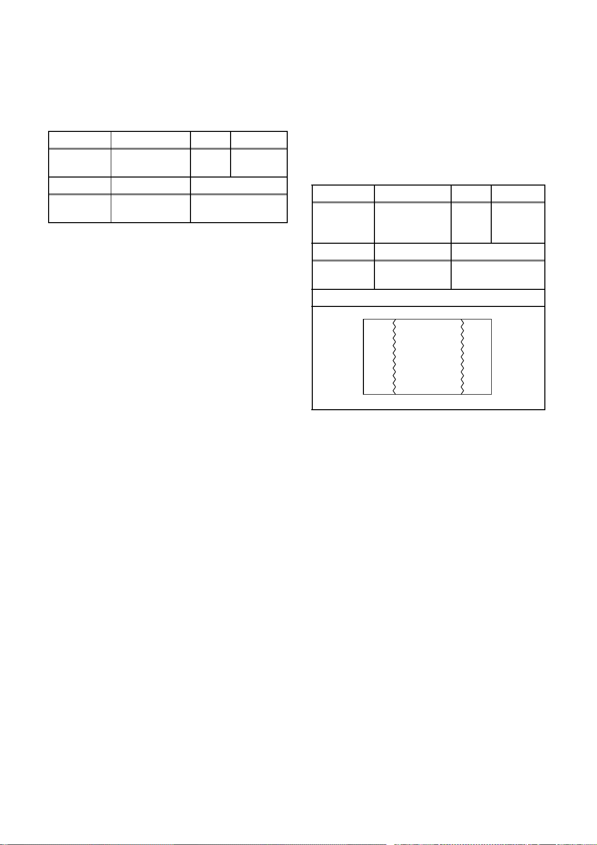
13. Focus Adjustment
Purpose: Set the optimum Focus.
Symptom of Misadjustment: If Focus Adjustment is
incorrect, blurred images are shown on the display.
Test Point Adj. Point Mode Input
--- Focus Control ---
Tape M. EQ. Spec.
---
Focus VR (FBT) - Main CBA FBT=Fly Bac k Transformer
Note:
1. Operate the unit more than 30 minutes
2. Face the unit to the East and Degauss the CRT
using Degaussing Coil.
3. Input the Monoscope Pattern.
4. Adjust the Focus Control on the FBT to obtain
clear picture.
Pattern
Generator
Mono-
scope
See below
The following 2 adjustments normally are not
attempted in the field. Only when replacing the
CRT then adjust as a preparation.
14. Purity Adjustment
Purpose: To obtain pure color.
Symptom of Misadjustment: If Color Purity Adjust-
ment is incorrect, large areas of color may not be
properly displayed.
Test Point Adj. Point Mode Input
Deflection
---
Tape M. EQ. Spec.
---
GREEN RED BLUE
Yoke Purity
Magnet
Pattern
Generator
Figure
---
See below.
Red
Color
Fig. 5
1. Set the unit facing east.
2. Operate the unit for over 30 minutes before adjusting.
3. Fully degauss the uni t using an external degaussing coil.
4. Loosen the screw on the Deflection Yoke Clamper
and pull the Deflection Yo ke back away from the
screen. (See Fig. 6)
5. Lo osen the Ring Lock and adj ust the Purit y Magnets so that a red fi eld is ob tai ned at t he c en ter of
the screen. Tighten Ring Lock. (See Fig. 5,6)
6. Slowly push the Deflection Yoke toward bell of
CRT and set it where a uniform red field is obtained.
7. Tighten the clamp screw on the Deflection Yoke.
5-6 L6605EA
Page 20
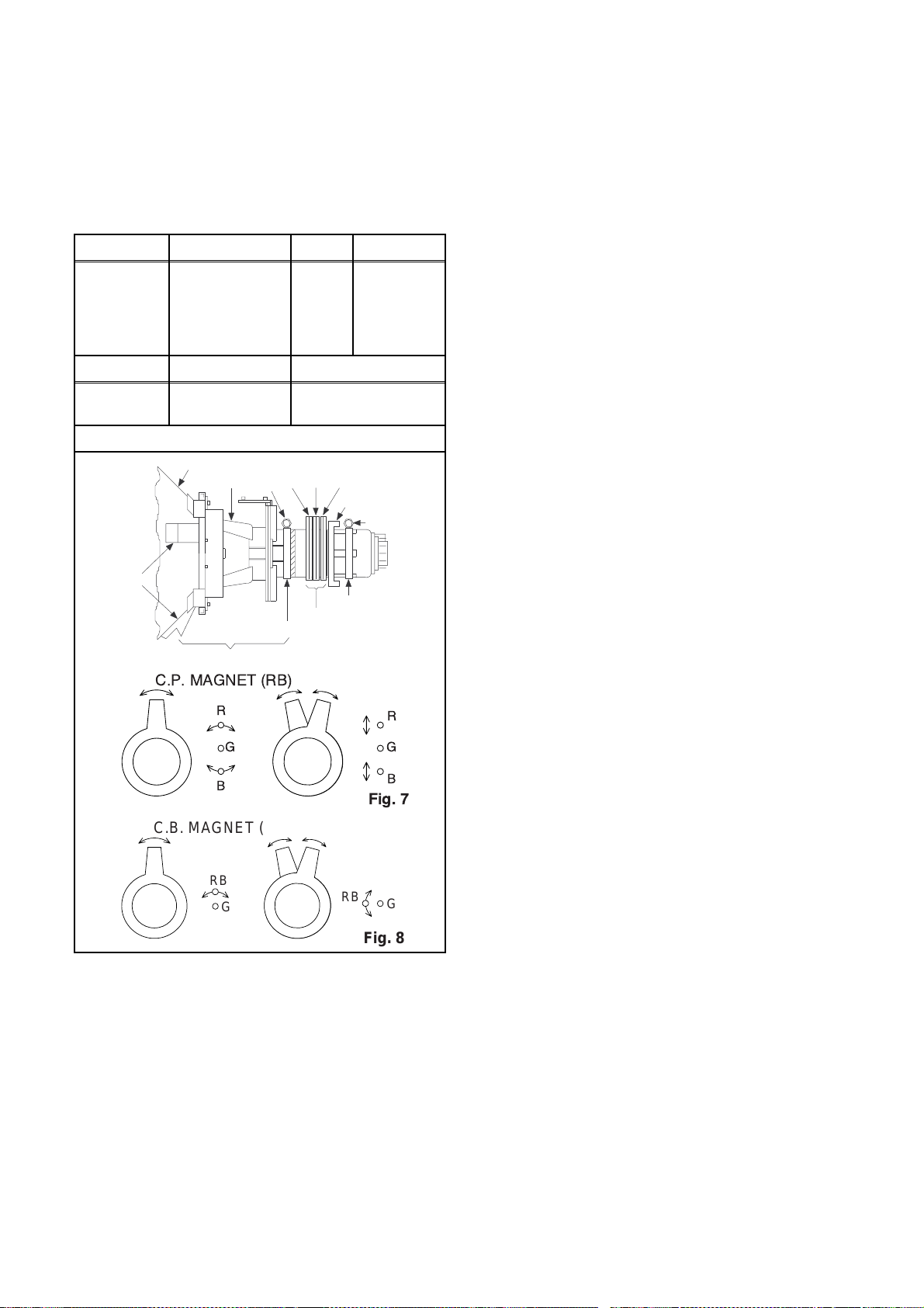
15. Convergence Adjustment
Purpose: To o btain p roper convergence of re d, green
and blue beams.
Symptom of Misadjustment: If Convergence Adjustment is incorrect, the edge of white letters may have
color edges.
Test Point Adj. Point Mode Input
C.P. Magnet
(RB),
---
C.P. Magnet
---
(RB-G),
Deflection Yoke
Tape M. EQ. Spec.
Dot Pattern
or
Crosshatch
1. Loosen the Ring Lock and align red with blue dots
or Crosshatch at the center of the screen by rotating (RB) C.P. Magnets. (See Fig. 7)
2. Align red / blue with green dots at the center of the
screen by rotating (RB-G) C.P. Magnet. (See Fig. 8)
3. Fix the C.P. Magnets by tightening the Ring Lock.
4. Remov e the DY Wedges and slightly tilt the Deflection Yoke horizontal ly and vertically to obtain
the best overall convergence.
5. F ix the Deflection Yoke by carefully inserting the
DY Wedges between CRT and Deflection Yoke.
---
DY WEDGE
Pattern
Generator
CRT
DEFLECTION YOKE
C.B. MAGNET (RB-G)
Figures
COIL
PURITY
SCREW
COIL CLAMPER
See below.
RB-GRB
RING LOCK
SCREW
C.P. MAGNET CLAMPER
C.P. MAGNET
Fig. 6
RB
RB
G
G
Fig. 8
5-7 L6605EA
Page 21
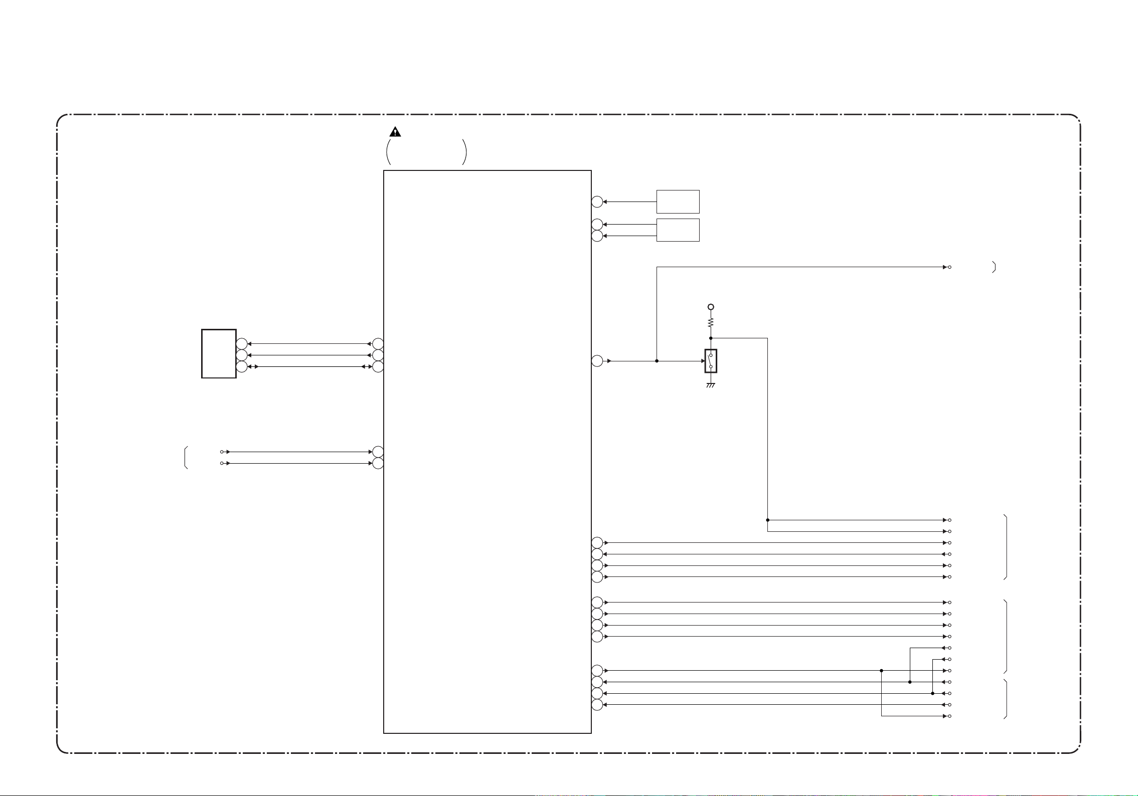
System Control Block Diagram
IC111
TV MICON/VIDEO
/AU
DIO/CHROMA
/DEFLECTION
BLOCK DIAGRAMS
RCV-IN
70
RCV101
REMOTE
SENSOR
FROM/TO
IF/VIDEO BLOCK
IC151
(MEMORY)
CS
SCL
SDA 5
AFT
AGC
KEY-IN1
KEY-IN2
7
6
72 I2C-OPEN
58
SCL
56
SDA
73
AFT
75
AGC-IN
INPUT0
66
69
63
KEY
SWITCH
+8V
Q481
INPUT0
TO
IF/VIDEO BLOCK
MAIN CBA
6-1 6-2
MONO-OUT
STEREO-IN
VOLUME
DG-ON-H
+5V-CTRL
+5V-CTRL2
+8V-CTRL
P-ON-H
PROTECT-1
PROTECT-2
PROTECT-3
71
60
62
64A-MUTE-H
74
28
18
40
79
68
67
76
INSEL1
INSEL2
MONO-OUT
STEREO-IN
VOLUME
A-MUTE-H
DG-ON-H
+5V-CTRL
+5V-CTRL2
+8V-CTRL
PROTECT-1
PROTECT-2
P-ON-H
PROTECT-1
PROTECT-2
PROTECT-3
P-ON-H
FROM/TO
AU
DIO BLOCK
FROM/TO
POWER
SUPPLY BLOCK
FROM/TO
CRT/H.V. BLOCK
L6605BLS
Page 22
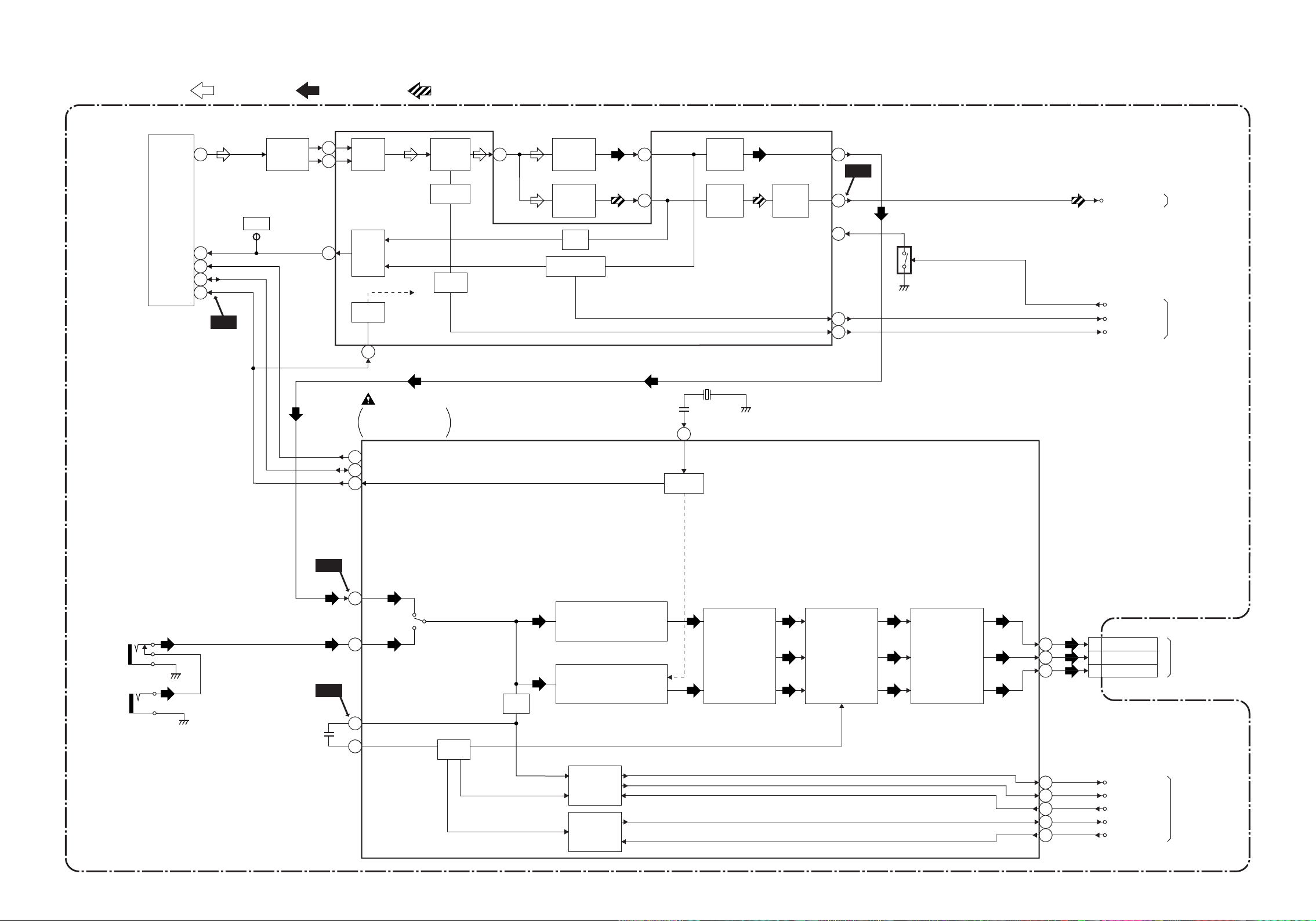
IF/Video Block Diagram
TU1
EXT.CLK
AGC
SCL
SDA
VIDEO SIGNALRF/IF SIGNAL
SF1
IF
11
1
4
5
8
WF16
SAW
FILTER
TP301
AGC
IC31 (IF SIGNAL PROCESS)
20
VIF
AMP
21
RF
17
AGC
AMP
14
IC111
TV MICON/VIDEO
/AU
DIO/CHROMA
/DEFLECTION
AUDIO SIGNAL
VIDEO
DET
VCO
AFT
5
CF31
4.5MHz
TRAP
CF32
4.5MHz
FILTER
LPF
IF AGC DET
MAIN CBA
16
EQ
AMP
FM
DET
X301
3.58MHz
AF
AMP
VCO F/B
11
22
16
1
WF6
TU-AUDIO
7
Q31
INPUT0
AGC
AFT
TO
AUDIO BLOCK
FROM/TO
SYSTEM
CONTROL
BLOCK
3
8
JK701
VIDEO-IN
(FRONT)
JK704
VIDEO-IN
(REAR)
WF1
WF2
58
56
32
26
24
14
11
SCL
SDA
TUNER
LINE
OSD
LPF
LUMINANCE
PROCESS
CIRCUIT
CHROMINANCE
PROCESS
CIRCUIT
H-SYNC
PROCESS
CIRCUIT
V-SYNC
PROCESS
CIRCUIT
VCXO
RGB MATRIX
/COLOR CONT
OSD SW
CONTRAST
BRIGHTNESS
RGB DRIVE
/CUT OFF
/H.V. BLK
52
51
50
53
46
45
38
37
WH301A
BLUE5
GREEN4
RED3
ACL
H-DRIVE
FBP
RAMP-OUT
V-RAMP-F/B
TO
CRT/H.V. BLOCK
WH301B
FROM/TO
CRT/H.V. BLOCK
L6605BLIF6-3 6-4
Page 23
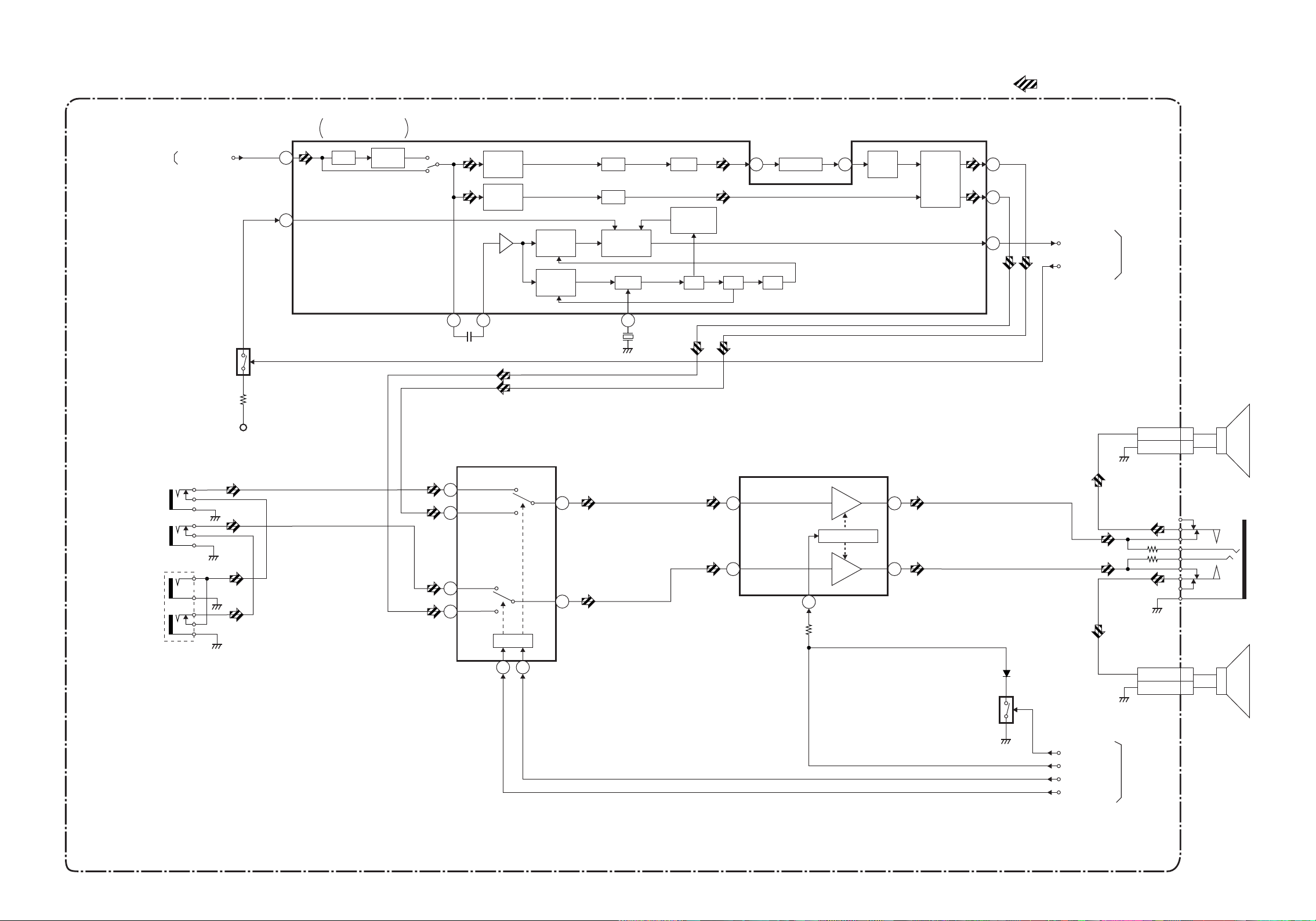
Audio Block Diagram
AUDIO SIGNAL
FROM
IF/VIDEO BLOCK
JK702
AUDIO-IN-(L)
NT)
(FRO
JK703
AUDIO-IN-(R)
NT)
(FRO
TU-AUDIO
+8V
Q441
5
21
MTS/SAP AUDIO
SIGNAL PROCESS
IC401
ATT
5fH
TRAP
L-R
DEMOD
L+R
AMP
1
2
IC481 (INPUT SELECT)
FRONT
12
TUNER
11
(L-CH)
MAIN CBA
PILOT
DET
PHASE
COMP
13
LPF
LPF
STEREO
DRIVER
VCO F/F
22
X441
VCA
STEREO
SW
Q411
BUFFER
F/F F/F
IC802 (AUDIO AMP)
5
DC VOL.
L-R
AMP
141110
MATRIX
13
20
7
STEREO-IN
MONO-OUT
FROM/TO
SYSTEM
CONTRO
BLOCK
CN801
SP-L
SP-GND
L
1
2
JK801
HEADPHONE
JAC
SP801
SPEAKER
L-CH
K
JK704
DIO-IN-(L)
AU
(REAR)
JK704
DIO-IN-(R)
AU
(REAR)
12
1
4
(R-CH)
FRONT
TUNER
SW CTL
9 10
2
3
6
6-5 6-6
Q825
A-MUTE-H
VOLUME
INSEL1
INSEL2
CN802
SP-R 1
SP-GND 2
FROM
SYSTEM
CONTRO
BLOCK
SP802
SPEAKER
R-CH
L
L6605BLA
Page 24
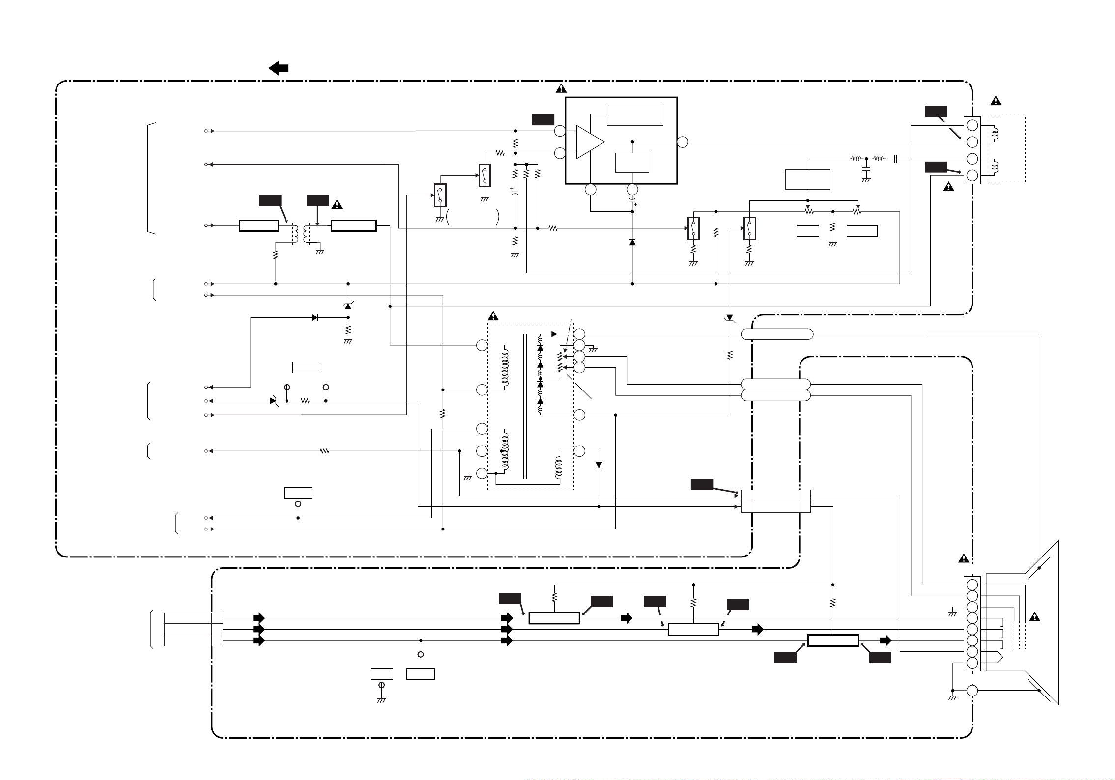
CRT/H.V. Block Diagram
RAMP-OUT
FROM/TO
IF/VIDEO BLOCK
V-RAMP-F/B
H-DRIVE
VIDEO SIGNAL
MAIN CBA
WF7 WF8
Q572 Q571
H.DRIVE
T572
H.OUTPUT
Q531
(SWITCHING)
Q532
SWITCHING
P-ON-ON
WF11
IC551 V-DEFLECTION CONTROL
THERMAL
PROTECTION
7
AMP
1
6 3
PULSE
UP
Q561
(SWITCHING)
5
4
3
1
DY551 D.Y.
VDRIVE
HDRIVE
WF12
5
Q551,
H.
Q552
CONTROL
Q553
(SWITCHING)
PCC WIDTH
VR562VR561
WF9
CN571
FROM POWER
SUPPLY BLOCK
FROM/TO
SYSTEM CONTRO
BLOCK
TO
SYSTEM CONTROL
BLOCK
FROM/TO
IF/VIDEO BLOCK
FROM
IF/VIDEO BLOCK
L
DEF+B
+B
PROTECT-1
PROTECT-2
P-ON-H
PROTECT-3
FBP
ACL
RED
GREEN 4
BLUE 5
RED AMP
FOCUS VR
HV
11
F
S
SCREEN VR
8
3
WF15
WF4
WF10
Q1522
GREEN AMP
ANODE
FOCUS
SCREEN
HEATER3 3
1 1
+180V
WF14
WH501BWH501A
Q1532
BLUE AMP
WF5 WF13
JK1501
7
4
8
6
11
10
9
CN1501
ANODE
FOCUS
SCREEN
GND
R
G
B
HEATER
GND
V501
CRT
T571 F.B.T.
1
X-RAY
TP591 TP592
5
10
4
TP302
15kHz
WH301BTO WH301A
3
TP1501
GND
TP1502
BLUE
7
WF3
Q1512
6-7 6-8
CRT CBA
L6605BLCRT
Page 25
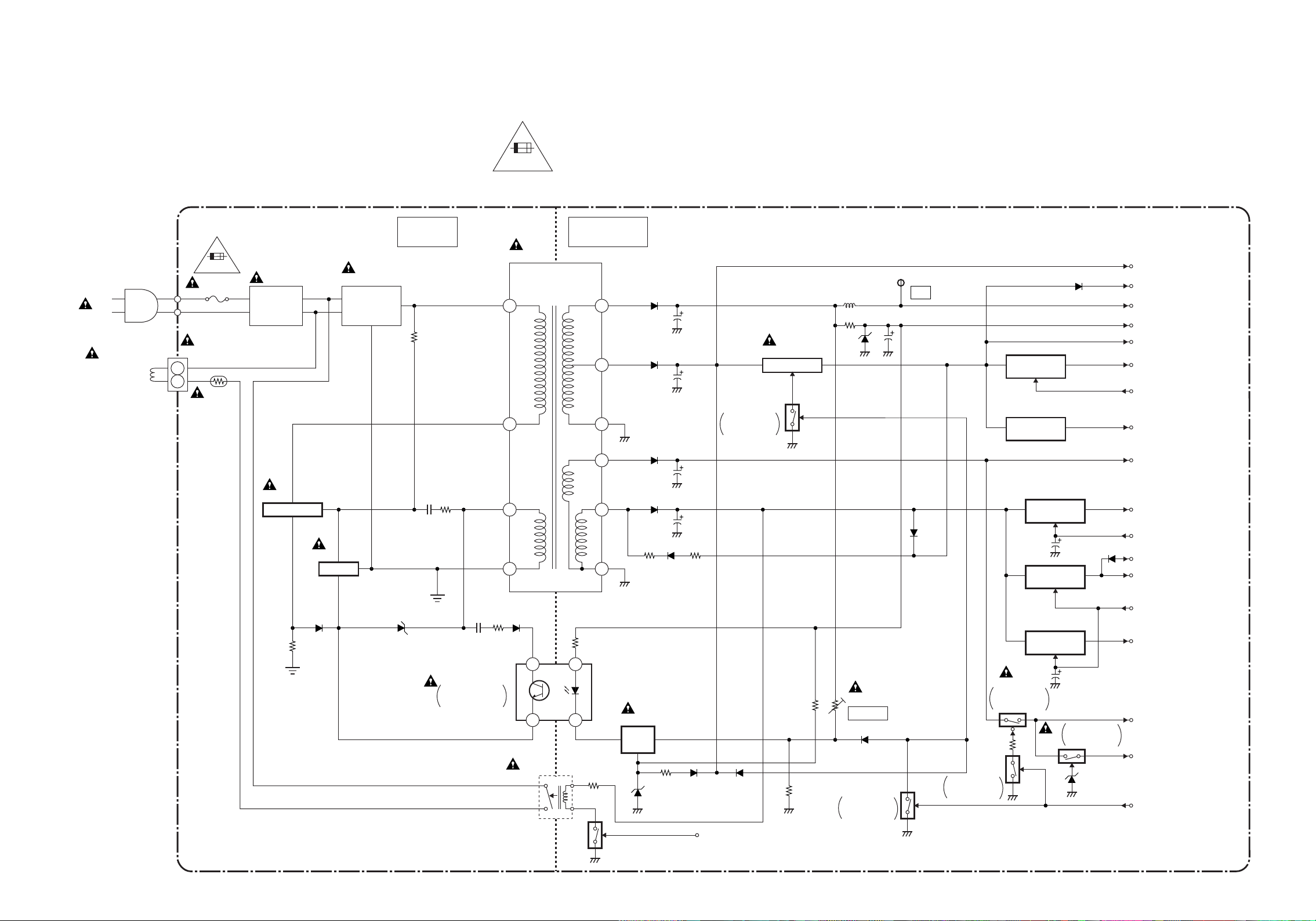
Power Supply Block Diagram
CAUTION !
Fixed voltage ( or Auto voltage selectable ) power supply circuit is used in this unit.
If Main Fuse (F601) is blown, check to see that all components in the power supply
circuit are not defective before you connect the AC plug to the AC power supply.
Otherwise it may cause some components in the power supply circuit to fail.
HOT CIRCUIT. BE CAREFUL.
HOT COLD
4A/125V
CAUTION:
FOR CONTINUED PROTECTION AGAINST RISK OF FIRE,
REPLACE ONLY WITH SAME TYPE 4 A, 125V FUSE.
ATTENTION: UTILISER UN FUSIBLE DE RECHANGE DE MÊME TYPE DE 4A, 125V.
NOTE :
The voltage for parts in hot circuit is measured using
hot GND as a common term
inal.
AC601
AC CORD
DG691
DEGAUSSING
COIL
CN691
4A/125V
F601
4A/125V
PS691
L601
LINE
FILTER
Q601
SWITCHING
Q602
LIMITER
D605 - D608
BRIDGE
RECTIFIER
T601
6
10
4
2
1 13
11
12
14
DEF +B
TP601
+B
9
Q671
SWITCHING
Q676
SWITCHING
CONTRO
L
Q111
+5V
SWITCHING
Q321
+9V
SWITCHING
Q681
+8V
SWITCHING
Q682
+5V
SWITCHING
PROTECT-2
(TO PIN 67 OF IC111)
+B
AL+33V
BACK-UP
P-ON+5V
+5V CTRL2
(FROM PIN 18 OF IC111)
AL+9V
AL+12V
P-ON+8V
+8V CTRL
(FROM PIN40 OF IC111)
PROTECT-1
(TO PIN68 OF IC111)
P-ON+5V
6-9 6-10
IC601
ERROR
LTAGE DET
VO
4
3
RL601
+5V CTRL
Q683
+5V
SWITCHING
1
Q831
VR661
2
Q662
FEED
BACK
Q696
(SWITCHING)
DG-ON-H
M PIN74 OF IC111)
(FRO
+B ADJ
Q675
SWITCHING
P-ON-ON
SWITCHING
P-ON-ON
SWITCHING
P-ON-ON
Q832
MAIN CBA
Q833
SWITCHING
P-ON+8V
(FROM PIN28 OF IC111)
P-ON+5V
P-ON+12V
P-ON+8V
P-ON-H
(FRO
M PIN79 OF IC111)
L6605BLP
Page 26
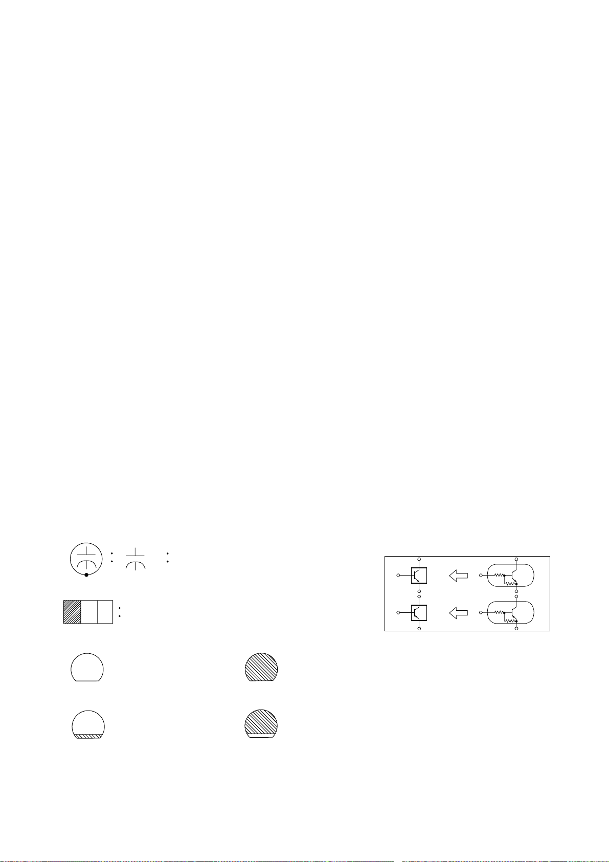
SCHEMATIC DIAGRAMS / CBA'S AND TEST POINTS
Standard Notes
Many electrical and mechanical parts in this chassis have special characteristics. These characteristics often
pass unnoticed and the protection afforded by them cannot necessarily be obtained by using replacement components rated for higher voltage, wattage, etc. Replacement par ts that have these special safety character ist ics ar e
identified in this ma nual and its supplements; electr ical components having such features are ident ified by the
mark " # " in the schematic diagram and the parts list. Before replacing any of these components, read the parts
list in this manual carefully. The use of substitute replacement parts that do not have the same safety characteristics as specified in the parts list may create shock, fire, or other hazards.
Note:
1. Do not use the part number show n on these drawings for orderi ng. The correct part numbe r is shown in the
parts list, and may be slightly different or amended since these drawings were prepared.
3
2. All resistance values are indicated in ohms (K=10
3. Resistor wattages are 1/4W or 1/6W unless otherwise specified.
4. All capacitance values are indicated in µF (P=10
5. All voltages are DC voltages unless otherwise specified.
Note of Capacitors:
ML --- Mylar Cap. PP --- Metallized Film Cap. SC --- Semiconductor Cap. L --- Low Leakage type
, M=106).
-6
µF).
Temperature Characteristics of Capacitors are noted with the following:
B --- ±10% CH --- 0±60ppm/°C CSL --- +350~-1000ppm/°C
Tolerance of Capacitors are noted with the following:
Z --- +80~-20%
Note of Resistors:
CEM --- Cement Res. MTL --- Metal Res. F --- Fuse Res.
Capacitors and transistors are represented by the following symbols.
CBA Symbols
(Top View) (Bottom View)
+
(Bottom View)
Transistor or Digital Transistor
E C B
(Top View)
NPN Transistor
Electrolytic Capacitor
(Top View)
PNP Transistor
Schematic Diagram Symbols
Digital Transistor
E C B
(Top View)
NPN Digital Transistor
E C B
E C B
(Top View)
PNP Digital Transistor
E C B
7-1 L13SC
Page 27
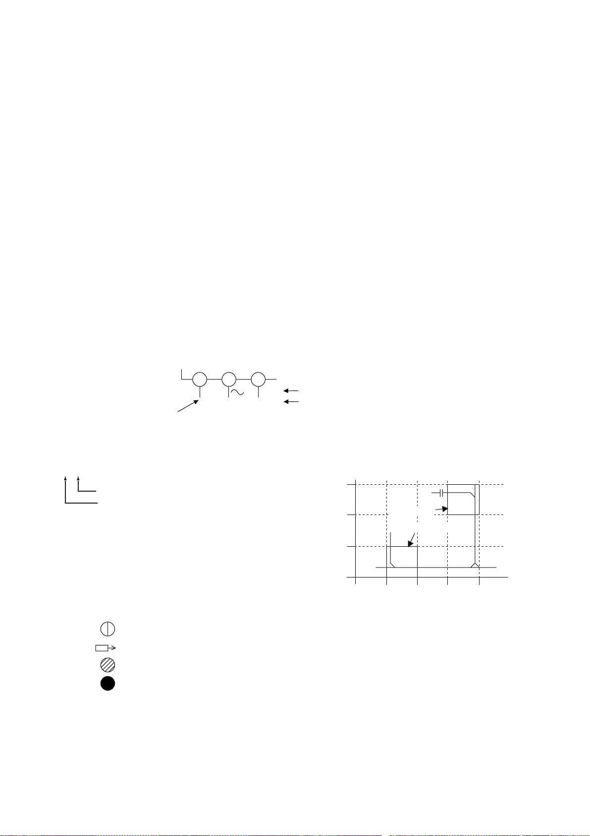
LIST OF CAUTION, NOTES, AND SYMBOLS USED IN THE SCHEMATIC DIAGRAMS ON
THE FOLLOWING PAGES:
1. CAUTION: FOR CONTINUED PROTECTION AGAINST RISK OF FIRE, REPLACE ONLY WITH SAME
TYPE_A,_V FUSE.
ATTENTION: UTILISER UN FUSIBLE DE RECHANGE DE MÊME TYPE DE_A,_V.
2. CAUTION:
Fixed Voltage (or Auto voltage selectable) power supply circuit is used in this unit.
If Main Fuse (F601) is blown, first check to see that all components in the power supply circuit are not defective
before you connect the AC plug to the AC power supply. Otherwise it may cause some components in the power supply circuit to fail.
3. Note:
(1) Do not use the part number shown on the dra wings for ordering. The correc t part number is shown in the
parts list, and may be slightly different or amended since the drawings were prepared.
(2) To maintain origin al function and reli ability of r epaired u nits, use only origin al replacem ent parts whi ch are
listed with their part numbers in the parts list section of the service manual.
4. Wire Connectors
(1) Prefix symbol "CN" means "connector" (can disconnect and reconnect).
(2) Prefix symbol "CL" means "wire-solder holes of the PCB" (wire is soldered directly).
5. Note: Mark "I" is a leadless (chip) component.
6. Voltage indications on the schematics are as shown below:
Plug the TV power cord into a standard AC outlet.:
Voltage
7. How to read converged lines
1-D3
Distinction Area
Line Number
(1 to 3 digits)
Examples:
1. "1-D3" means that line number "1" goes to area "D3".
2. "1-B1" means that line number "1" goes to area "B1".
8. Test Point Information
: Indicates a test point with a jumper wire across a hole in the PCB.
: Used to indicate a test point with a component lead on foil side.
: Used to indicate a test point with no test pin.
5.0
(3.0)
231
5.0
(3.0)
Indicates that the voltage
is not consistent here.
Power on mode
Power off mode
Unit: Volts
3
AREA D3
2
1
ABCD
AREA B1
1-D3
1-B1
: Used to indicate a test point with a test pin.
7-2 L13SC
Page 28
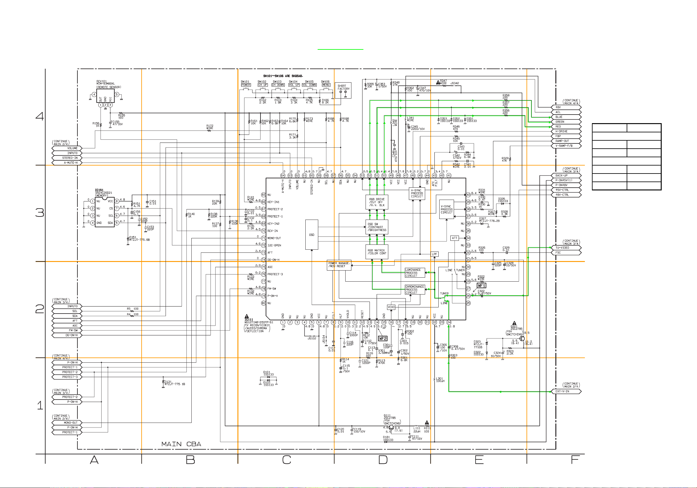
Main 1/4 Schematic Diagram
VIDEO SIGNAL
A4
A3
B4
B3
C4
C3
D4
D3
E4
E3
F4
F3
MAIN 1/4
Ref No. Position
ICS
IC111
IC151
TR ANSIST ORS
Q111 D-1
Q321 E-2
Q361 D-4
C-2
A-3
A2
A1
B2
B1
7-3 7-4
C2
C1
D2
D1
E2
E1
F2
F1
L6605SCM1
Page 29
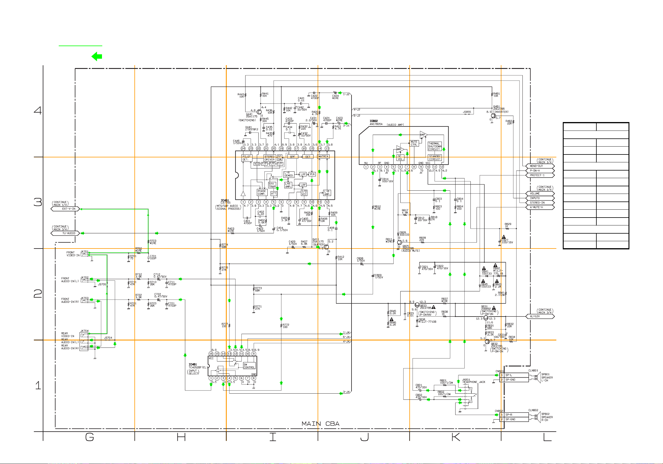
Main 2/4 Schematic Diagram
VIDEO SIGNAL
AUDIO SIGNAL
G4
G3
H4
H3
I4
I3
J4
J3
K4
K3
L4
L3
MAIN 2/4
Ref No. Position
ICS
IC401
IC481
IC802
TR ANSIST ORS
Q411
Q441
Q481
Q825
Q831
Q832
Q833
CONNECTO RS
CN801 K-1
CN802 K-1
H-3
H-1
J-4
I-3
I-4
K-4
J-3
K-2
K-1
K-2
G2
G1
7-5
H2
H1
I2
I1
J2
J1
K2
K1
7-6
L2
L1
L6605SCM2
Page 30
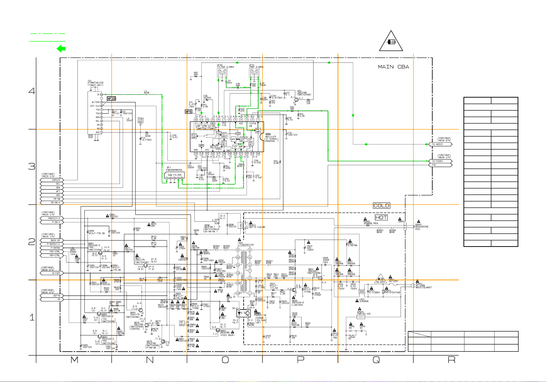
Main 3/4 Schematic Diagram
IF SIGNAL
VIDEO SIGNAL
AUDIO SIGNAL
CAUTION !
Fixed voltage ( or Auto voltage selectable ) power supply circuit is used in this unit.
If Main Fuse (F601) is blown, check to see that all components in the power supply
circuit are not defective before you connect the AC plug to the AC power supply.
Otherwise it may cause some components in the power supply circuit to fail.
NOTE :
The voltage for parts in hot circuit is measured
using hot GND as a common terminal.
4A/125V
CAUTION: FOR CONTINUED PROTECTION AGAINST RISK
OF FIRE, REPLACE ONLY WITH SAME TYPE 4A, 125V FUSE.
ATTENTION: UTILISER UN FUSIBLE DE RECHANGE DE
MÊME TYPE DE 4A, 125V.
M4
M3
M2
N4
N3
N2
O4
O3
O2
P4
P3
P2
Q4
Q3
Q2
R4
R3
R2
MAIN 3 /4
Ref No. Position
ICS
IC31
IC601
TR ANSIST ORS
Q31
Q601
Q602
Q641
Q662
Q671
Q675 N-1
Q676
Q681
Q682
Q683
Q696
CONNECTO R
CN691 Q-2
TEST PO IN T
TP301
VARIABLE R ESISTO R
VR661 O-1
P-3
O-1
P-4
P-2
P-1
N-1
O-1
N-2
N-1
M-1
M-1
M-1
O-2
N-4
M1
N1
7-7
O1
P1
Q1
1 NOTE:
*
The Capacitor ( C643 ) is either type A or type B.
These two types are exchangeable and can be
equally used whichever the model is . The difference
between type A and type B is shown in the table below.
Type A
Type B
7-8
R1
C643 C642 JS642
0.01/250V
4700P/250V
0.01/250V
Not Used
Not Used
WIRE
L6605SCM3
Page 31
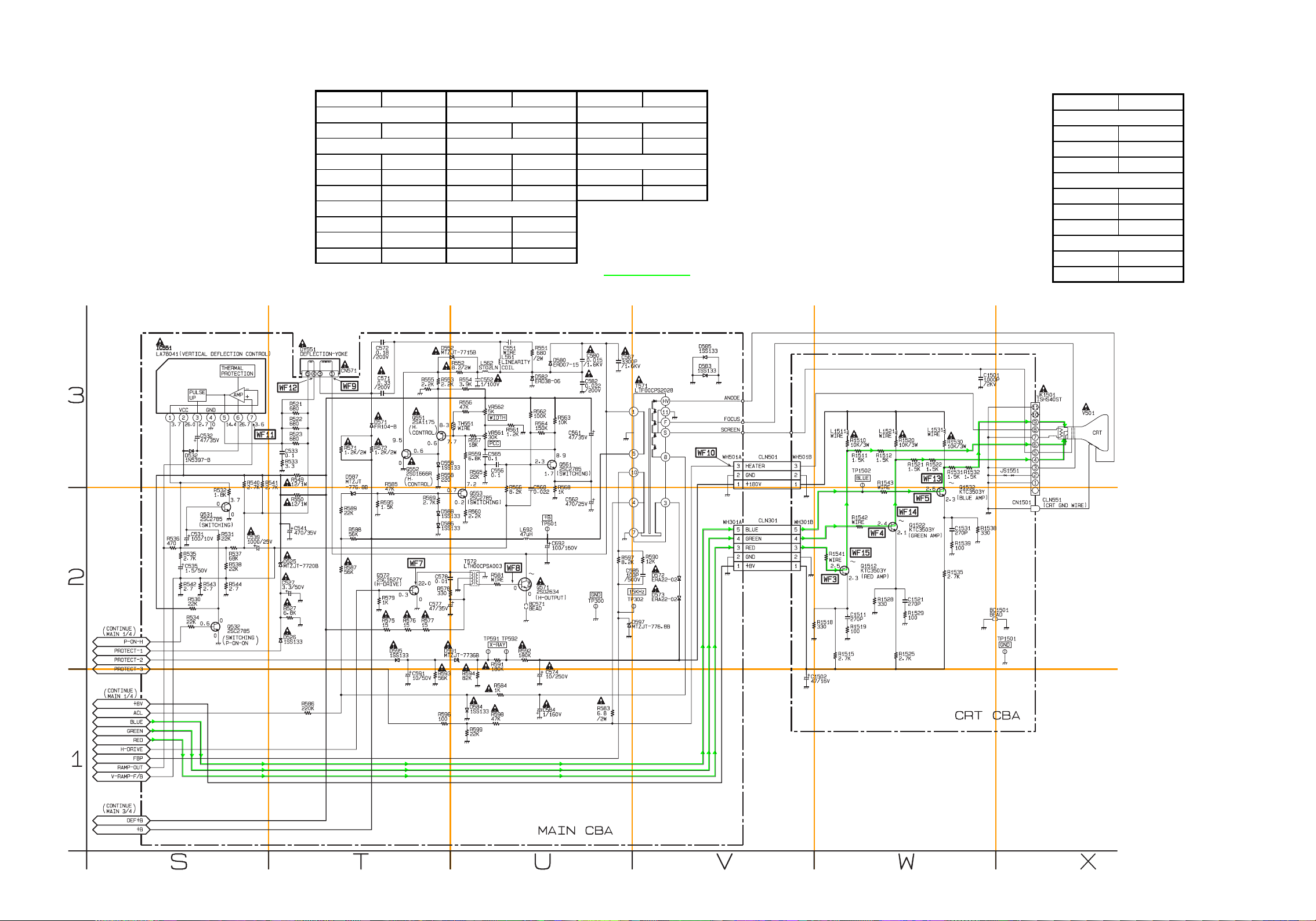
Main 4/4 & CRT Schematic Diagram
S3
MAIN 4/4
Ref No. Position Ref No. Position Ref No. Position
IC
IC551
TR AN SISTO RS C O N N EC T ORS
Q531
Q532
Q551 T-3 WH501A V-3 VR562 U-3
Q552 T-3
Q553
Q561 U-3 TP302 V-2
Q571 U-2 TP591 U-2
S-3
S-2
S-2 WH301A V-2 VR561 U-3
U-2
T3
TR AN SISTO RS TEST POINTS
Q572
CN571
TEST PO IN TS
TP300
T-2
T-3
U-2
TP592
TP601
VARIABLE R ESISTO R S
U3
U-2
U-2
VIDEO SIGNAL
V3
W3
CRT
Ref No. Posit i o n
TR ANSISTOR S
Q1512
Q1522
Q1532
CONNECTO RS
CN1501 X-2
WH301B V-2
WH501B V-3
TEST PO IN TS
TP1501
TP1502 W-3
X3
W-2
W-2
W-2
X-2
S2
S1
7-9
T2
T1
U2
U1
V2
V1
W2
W1
7-10
X2
X1
L6605SCM4
Page 32
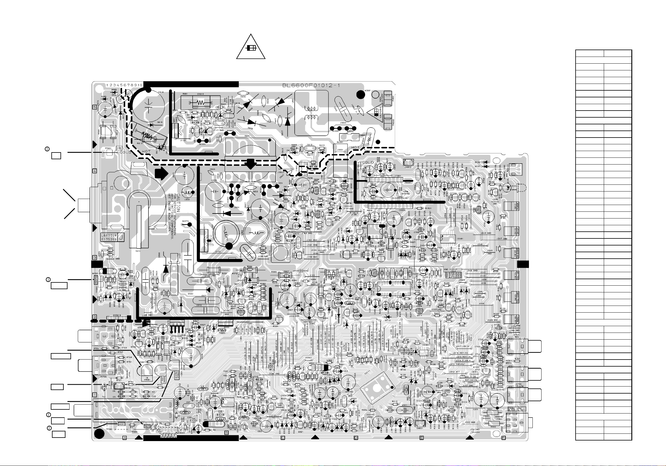
Main CBA Top View
CAUTION !
Fixed voltage ( or Auto voltage selectable ) power supply circuit is used in this unit.
If Main Fuse (F601) is blown, check to see that all components in the power
supply circuit are not defective before you connect the AC plug to the AC power supply.
Otherwise it may cause some components in the power supply circuit to fail.
TP601
+B
FOCUS-VR
(UPPER SIDE)
SCREEN-VR
(LOWER SIDE)
TP302
15kHz
VR661
+B ADJ
VR561
PCC
VR562
WIDTH
TP300
GND
TP301
AGC
4A/125V
CAUTION: FOR CONTINUED PROTECTION AGAINST RISK
OF FIRE, REPLACE ONLY WITH SAME TYPE 4A, 125V FUSE.
ATTENTION: UTILISER UN FUSIBLE DE RECHANGE DE
MÊME TYPE DE 4A, 125V.
NOTE :
The voltage for parts in hot circuit is measured
using hot GND as a common terminal.
BECAUSE A HOT CHASSIS GROUND IS PRESENT IN THE POWER
SUPPLY CIRCUIT, AN ISOLATION TRANSFORMER MUST BE USED.
ALSO, IN ORDER TO HAVE THE ABILITY T O INCREASE THE INPUT
SLOWL Y , WHEN TR OUBLESHOOTING THIS TYPE POWER SUPPL Y
CIRCUIT, A VARIABLE ISOLATION TRANSFORMER IS REQUIRED.
MAIN CBA
Ref No. Posi tio n
ICS
IC31
IC111
IC151
IC401
IC481
IC551
IC601
IC802
TRANSISTORS
Q31 C-1
Q111 D-2
Q321 C-1
Q411 E-2
Q441 D-3
Q481 F-2
Q531
Q532
Q551
Q552
Q553
Q561
Q571
Q572
Q601
Q602
Q641
Q662
Q671
Q675
Q676
Q681
Q682
Q683
Q696
Q825
Q831
Q832
Q833
CONNECTORS
CN571
CN691
CN801
CN802
WH301A C-2
WH501A A-3
TEST POINTS
TP300
TP301
TP302 A-3
TP591 A-3
TP592 A-3
TP601
VARIABLE RESISTORS
VR561
VR562
VR661 B-2
B-1
D-2
E-2
D-3
E-3
B-2
C-4
E-4
B-2
A-2
B-2
B-2
B-2
C-2
B-4
C-3
B-5
B-5
D-4
D-4
D-4
D-4
D-4
D-2
D-3
D-2
D-4
D-4
D-3
D-3
E-4
B-3
D-5
E-1
E-4
A-1
A-1
A-4
B-2
B-2
7-11
7-12
BL6600F01012-1
Page 33
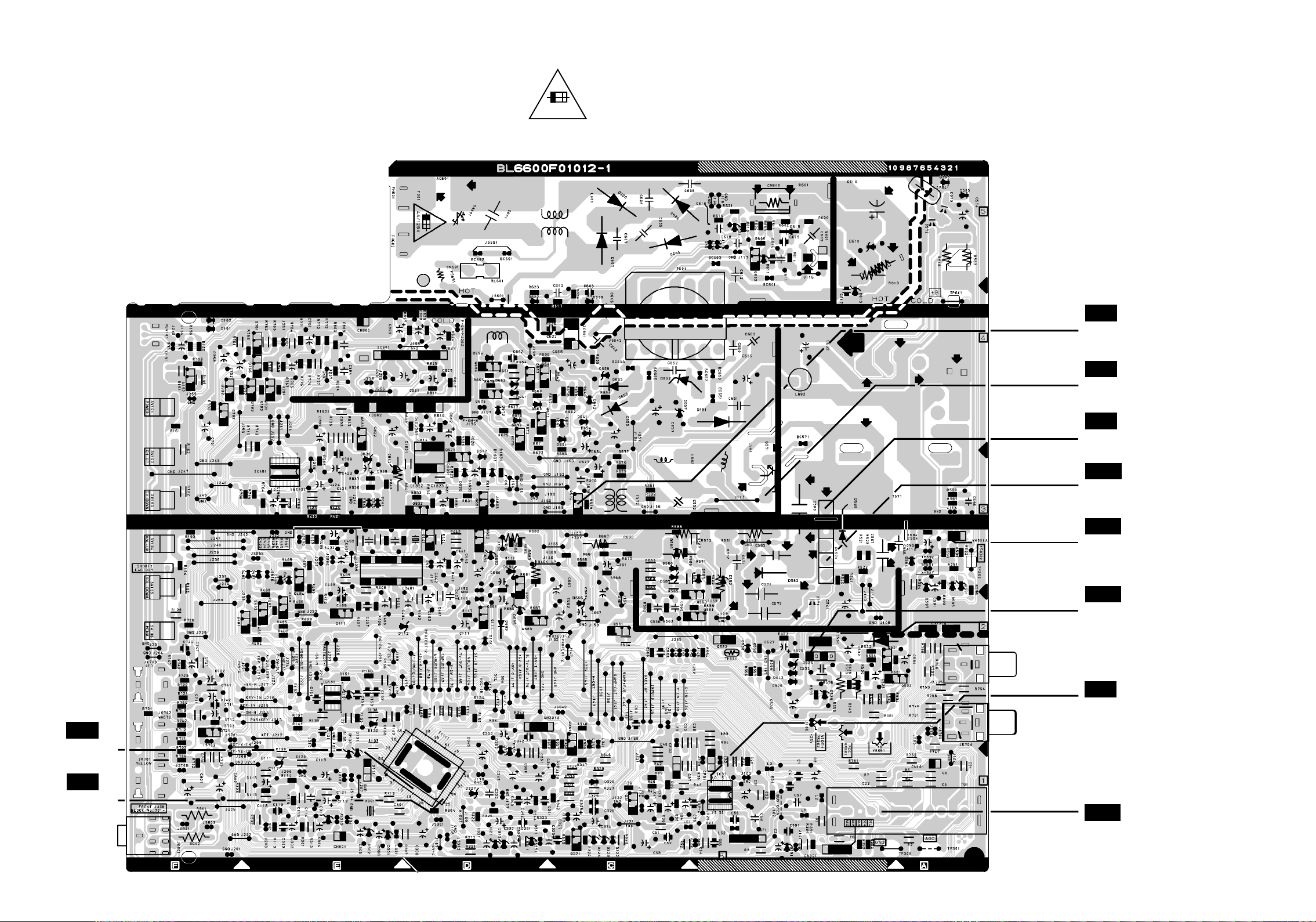
Main CBA Bottom View
CAUTION !
Fixed voltage ( or Auto voltage selectable ) power supply circuit is used in this unit.
If Main Fuse (F601) is blown, check to see that all components in the power supply
circuit are not defective before you connect the AC plug to the AC power supply.
Otherwise it may cause some components in the power supply circuit to fail.
4A/125V
CAUTION: FOR CONTINUED PROTECTION AGAINST RISK
OF FIRE, REPLACE ONLY WITH SAME TYPE 4A, 125V FUSE.
ATTENTION: UTILISER UN FUSIBLE DE RECHANGE DE
MÊME TYPE DE 4A, 125V.
NOTE :
The voltage for parts in hot circuit is measured
using hot GND as a common terminal.
BECAUSE A HOT CHASSIS GROUND IS PRESENT IN THE POWER
SUPPLY CIRCUIT, AN ISOLATION TRANSFORMER MUST BE USED.
ALSO, IN ORDER TO HAVE THE ABILITY TO INCREASE THE INPUT
SLOWL Y , WHEN TROUBLESHOO TING THIS TYPE POWER SUPPL Y
CIRCUIT, A VARIABLE ISOLATION TRANSFORMER IS REQUIRED.
WF7
Q572
Collector
WF8
Q571
Base
WF2
PIN 14
OF IC111
WF9
PIN 1
OF CN571
WF12
PIN 4
OF CN571
WF10
PIN 3
OF WH501A
WF11
PIN 7
OF IC551
WF6
PIN 11
OF IC31
WF1
PIN 26
OF IC111
7-13 7-14
WF16
PIN 8
OF TU1
BL6600F01012-1
Page 34
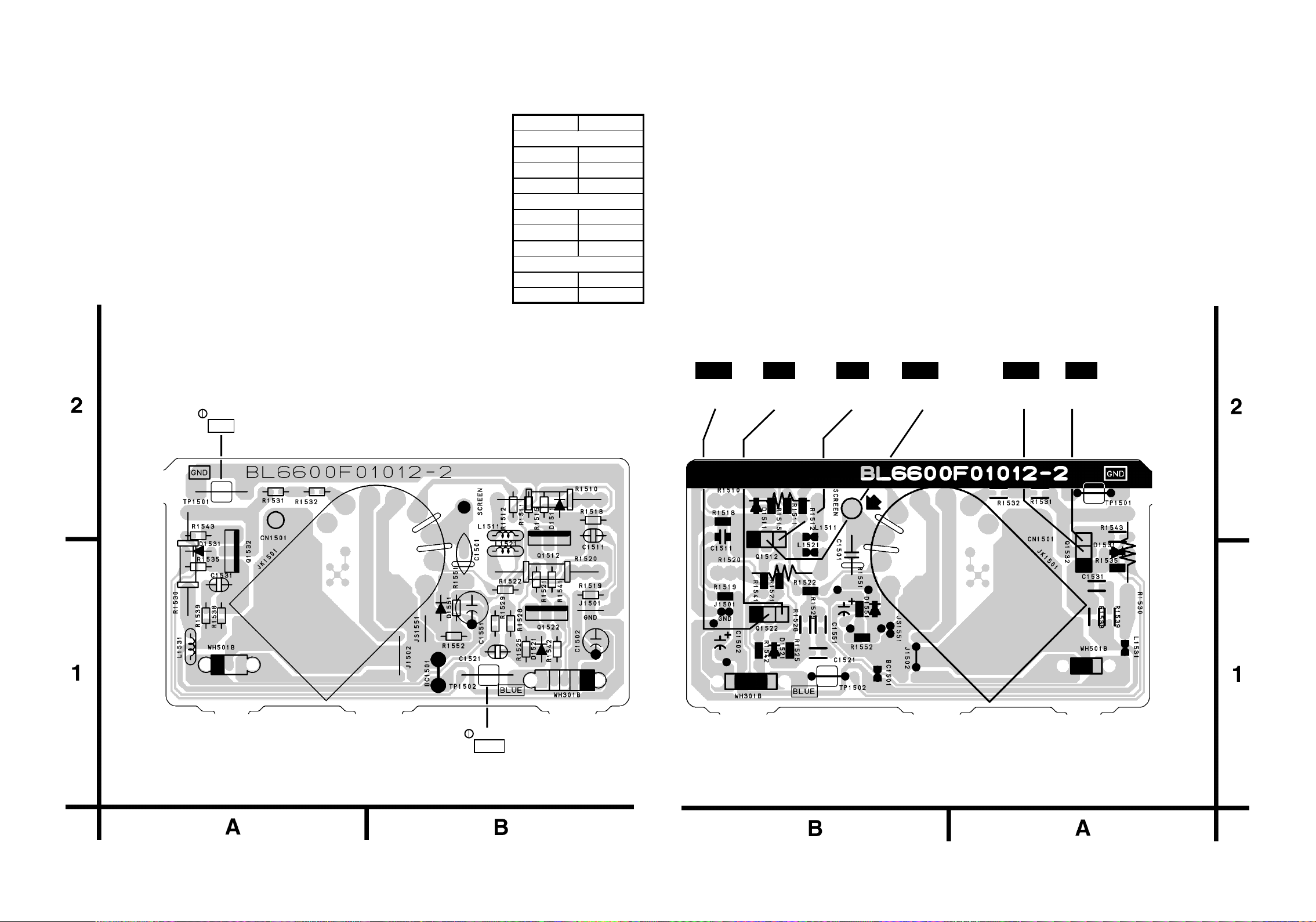
CRT CBA Top View CRT CBA Bottom View
CRT CBA
Ref No. Position
TR ANSIST ORS
Q1512 B-1
Q1522
Q1532
CONNECTO RS
CN1501 A-2
WH301B B-1
WH501B A-1
TEST PO IN TS
TP1501
TP1502 B-1
B-1
A-1
A-2
TP1501
GND
Q1522
Collector
WF4 WF13
Q1522
Base
WF3WF14
Q1512
Base
WF15
Q1512
Collector
Q1532
Collector
WF5
Q1532
Base
7-15 BL6600F01012-27-16
TP1502
BLUE
Page 35
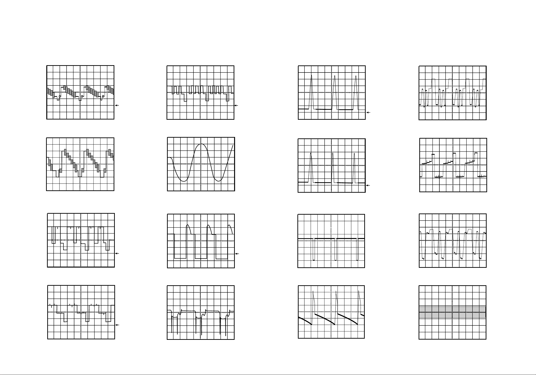
WF1 ~ WF16 = Waveforms to be observed at
Waveform check points.
(Shown in Schematic Diagram.)
WAVEFORMS
Input: NTSC Color Bar Signal (with 1kHz Audio Signal)
INITIAL POSITION: Unplug unit from AC outlet for at least 5 minutes.
reconnect to AC outlet and then turn power on.
(Brightness---Center Color---Center Tint --- Center Contrast---Approx 70%)
WF1
WF2
1DIV: 0.5V 20µsec
IC 111 Pin 26
1DIV: 0.5V 20µsec
IC 111 Pin 14
GND
WF5
WF6
1DIV: 2V 20µsec
Q 1532 Base
1DIV: 0.2V 20msec
IC 31 Pin 11
GND
WF9
WF10
1DIV: 200V 20µsec
CN 571 Pin 1
1DIV: 5V 20µsec
WH501A Pin 3
GND
GND
WF13
WF14
1DIV: 20V 20µsec
Q1532 Collector
1DIV: 20V 20µsec
Q 1522 Collector
GND
WF3
1DIV: 2V 20µsec
Q1512 Base
GND
WF4
1DIV: 2V 20µsec
Q 1522 Base
WF7
WF8
1DIV: 10V 20µsec
Q 572 Collector
1DIV: 5V 20µsec
Q 571 Base
GND
WF11
1DIV: 2V 5msec
IC 551 Pin 7
10 V 5 ms
WF12
1DIV: 10V 5msec
CN 571 Pin 4
WF15
WF16
1DIV: 20V 20µsec
Q 1512 Collector
1DIV: 0.2V 20µsec
TU 1 Pin 8
L6600WF8-1 8-2
Page 36
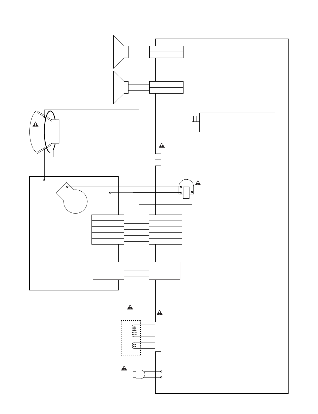
WIRING DIAGRAM
V501
CRT
GND
CN1501
ANODE
FOCUS
SP801
SPEAKER
L-CH
SP802
SPEAKER
R-CH
SCREEN
CLN801
CLN802
CN801
SP-L
1
SP-GND
2
CN802
SP-R
1
SP-GND
2
CN691
1
2
TU1 TUNER UNIT
MAIN CBA
BL6600F01012-1
T571
FBT
CRT CBA
BL6600F01012-2
WH301B
BLUE
GREEN
RED
GND
+8V
HEATER 3
GND 2
+180V 1
5
4
3
2
1
CLN301
CLN501
DY571
D.Y.
HD
VD
5
4
3
2
1
WH301A
BLUE
GREEN
RED
GND
+8V
WH501AWH501B
HEATER3
GND2
+180V1
CN571
1
2
3
4
5
AC601
9-1 L6605WI
Page 37
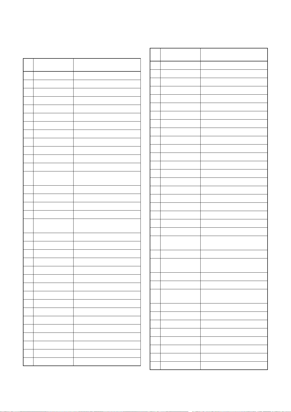
IC PIN FUNCTIONS
IC333 (TV Micro Computer)
Pin
Signal Name Function
No.
1GND GND
2 N.U. Not Used
3 N.U. Not Used
4 N.U. Not Used
5GND GND
6VCC AL+5V
7 N.U. Not Used
8 FILT FILT
9 HLF Filter for CCD
10 VHOLD VHOLD
11 CVIN Input for Video Signal
12 RESET RESET
MCU RESET
13
OUT
14 Y-SW OUT Composite Signal Output
15 GND GND
16 3.58 X'TAL 3.58MHz Crystal
17 C-APC CHROMINANCE APC
MCU 5.7REG
18
OUT
19 N.U. Not Used
20 CVBS IN 3 Composite Signal Input 3
21 N.U. Not Used
22 VCC VCC
23 N.U. (GND)
24 CVBS IN2 Composite Signal Input 2
25 N.U. Not Used
26 CVBS IN1 Composite Signal Input 1
27 N.U. Not Used
28 5.7V REG OUT 5.7V Output
29 C(Y/C) IN Chrominance Signal Input
30 Y(Y/C) IN Luminance Signal Input
31 V REG VCC DC 8.7V Input
32 FSC OUT Clock Output 3.58MHz
33 MONITOR OUT Monitor Out
34 N.U. Not Used
RESET Signal Output
Micro controller Control
Voltage Output
Pin
Signal Name Function
No.
35 N.U. Not Used
36 N.U. Not Used
37 V RAMP F/B V Ramp Feed Back
38 V RAMP OUT Vertical Output
39 V RAMP CAP V Ramp OSC Capacitor
40 8.7 VREG OUT DC 8.7V Output
41 N.U. Not Used
42 H VCO F/B H Vco Feed Back
43 AFC FILT Horizontal AFC Filter
44 GND GND
45 FBP IN Flyback Pulse Input
46 H-OUT H Pulse Output
47 VCC Vcc
48 VCC Vcc
49 VCC Vcc
50 R OUT Red Output
51 G OUT Green Output
52 B OUT Blue Output
53 ACL IB-Input
54 N.U. Not Used
55 A-O-MUTE Mute Signal of Audio Output
56 SDA
57 N.U. Not Used
58 SCL
59 N.U. (GND)
60 N.U. Not Used
61 S-SW
62 VOLUME Volume
63 INPUTO Input Select 0
64 A-MUTE-H Audio Mute
65 N.U. Not Used
66 KEY-IN 1 Key Input 1 (Main)
67 PROTECT-2 Power Supply Protection
68 PROTECT-1 Power Supply Protection
69 KEY-IN 2 Key Input 2 (Main)
I2C-BUS Controller Interface
(Data)
I2C-BUS Controller Interface
(Clock)
Detecting S-VIDEO Jack
Connection
10-1 L6650PIN
Page 38
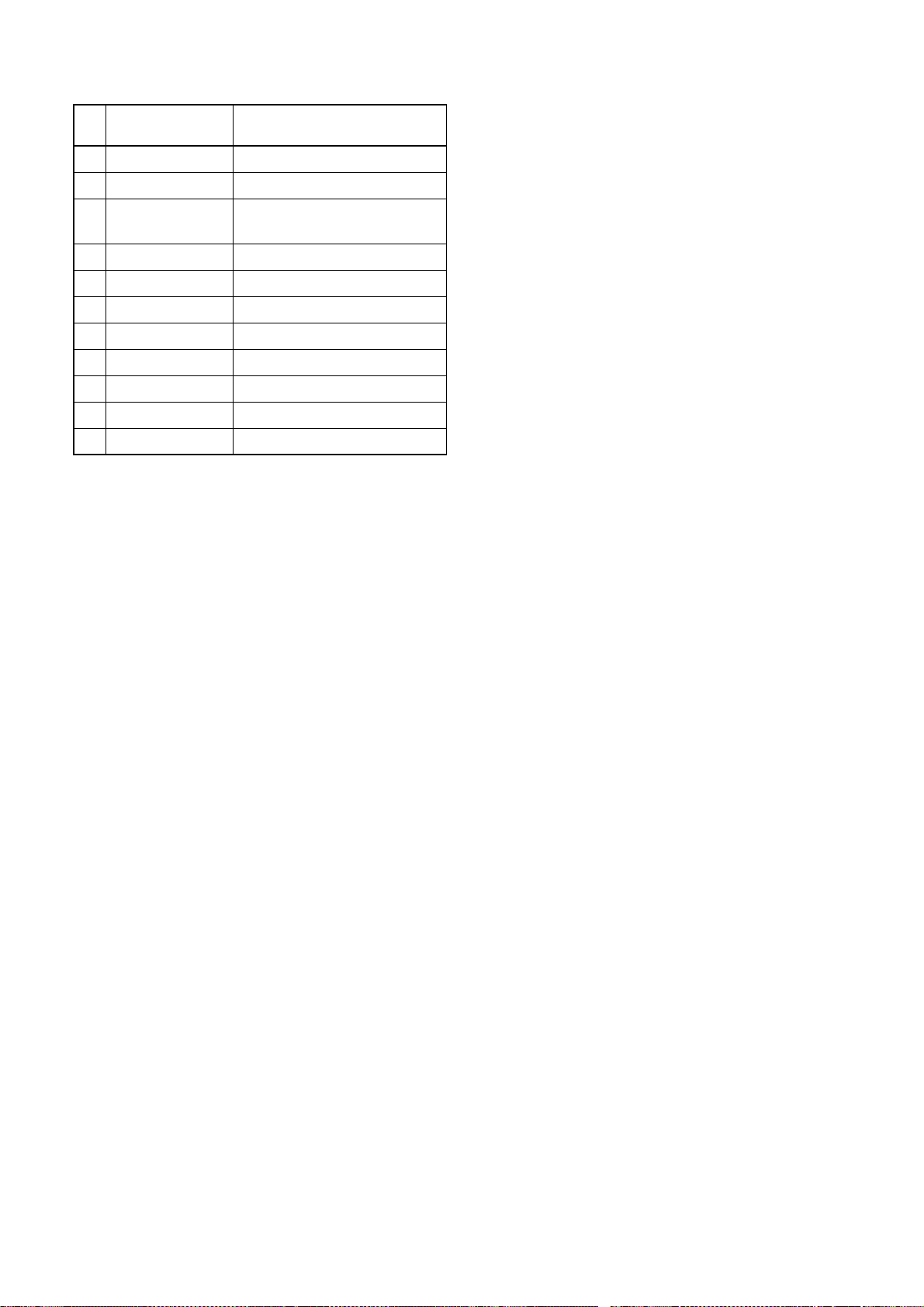
Pin
Signal Name Function
No.
70 RCV-IN Input For Remote Control
71 N.U. Not Used
72 I2C OPEN
73 AFT AFT Voltage Input
74 DG-ON-H Degaussing Coil Control
75 AGC AGC Voltage Input
76 PROTECT 3 Power Supply Protection
77 N.U. Not Used
78 FM-SW Switching IF IC VCO
79 P-ON-H Output for P-ON-H
80 INPU T 1 Input Select 1
White Balance Adjustm ent
Judgement
10-2 L6650PIN
Page 39
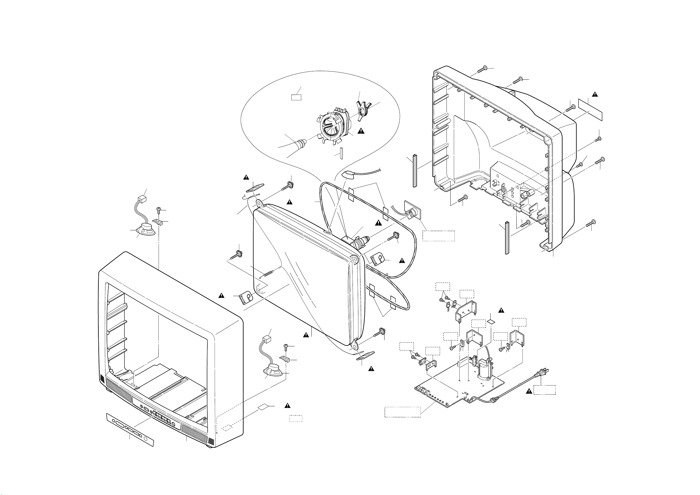
Cabinet
EXPLODED VIEWS
L2
SP801
B6
CLN801
Details for DY551
and surrounding parts
L1
B4
CLN551
B2
SHINWHA
TAPE SGT-730
(WHITE)
B3
SHINWHA
TAPE SGT-730
(BLACK)
B2
DG691
V501-2
V501-1
DY551
Scotch Tape #880
DY551
B2
B5
CRT CBA
L2
B5
L2
L2
L2
A5
L4
L3
L2
L2
B3
B1
CLN802
B6
B7
V501
L1
B4
SP802
See Electrical Parts List
for parts with this mark.
B3
Scotch Tape #880
B2
B3
MAIN CBA
L1
B1
L1
L1
B4
B3
A4
PB1
B2
L1
AC601
A2
11-1 11-2 L6601CEX
A1
Page 40
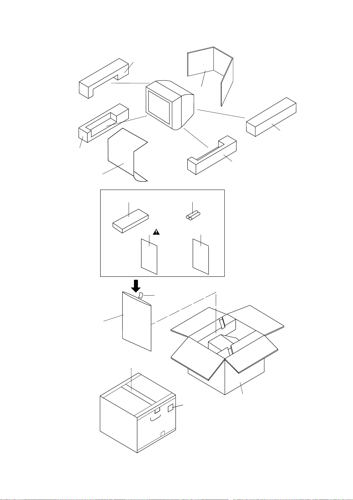
Packing
S2
S6
S2
S3
S3
S4
X1
X3
X2
PACKING TAPE
X4
X5
TAPE
S5
FRONT
11-3 L6601PEX
S1
Page 41
MECHANICAL PARTS LIST
PRODUCT SAFETY NOTE: Products marked with a #
have special characteristics important to safety. Before
replacing any of these components, read carefully the
product safety notice in this service manual. Don't
degrade the safety of the product through improper servicing.
NOTE:
Parts that are not assigned part numbers (---------) are
not available.
Ref. No. Description Part No.
A1 FRONT CABINET L6203UD 0EM000662
A2 CONTROL PLATE L6605CF 0EM301901
A4 REAR CABINET L6600UA or 0EM000690
REAR CABINET L6600UA 0EM101235
A5# RATING LABEL L6605CF ----------
B1 TENSION SPRING B0080B0:EM40808 26WH006
B2 M7 CRT SCREW(D22) T7205UF 0EM406573
B3# DEGAUSS HOLDER L1200UA 0EM405869
B4 SPEAKER HOLDER L1200UA 0EM405691
B5 CLOTH L9800UA:95X15XT:0.5 0EM405041
B6 CLOTH(10X30XT1.0) L9814UQ 0EM405137
B7# CRITICAL PARTS WARNING LABEL
CLN551 CRT GND WIRE CRT GND WX1L1200-007
CLN801 WIRE ASSEMBLY SPEAKER WIRE(180MM) WX1L9800-001
CLN802 WIRE ASSEMBLY SPEAKER WIRE(180MM) WX1L1131-001
DG691# DEGAUSSING COIL F-029 or LLBH00ZTM029
# DEGAUSSING COIL AVDG156 LLBH00ZWR043
SP801 SPEAKER S08N04 DSD0808XQ013
SP802 SPEAKER S08N04 DSD0808XQ013
L1 SCREW, P-TIGHT 3X12 BIND HEAD+ GBMP3120
L2 SCREW, P-TIGHT 4X18 BIND HEAD + GBMP4180
L3 SCREW TAPPING M4X14 DBU14140
L4 SCREW, P-TIGHT 3X10 BIND HEAD+ GBKP3100
B8007C3:EM41210
PAC KI NG
S1 CARTON L6605CF 0EM408292
S2 STYROFOAM TOP ASSEMBLY L6201UB 0EM407225
S3 STYROFOAM BOTTOM ASSEMBLY L6201UB 0EM407226
S4 SET SHEET PCEC:003502019816 0EM403887
S5 SERIAL NO. LABEL L6605CF ----------
S6 HOLD PAD L6201UB 0EM407287
S7 LABEL, EAS(H3761UD) MAKER NO.ZLLFNSLE1 ----------
ACCESSORIES
X1 POLYETHYLENE BAG 250X380XT0.03 Z325380
X2# OWNER'S MANUAL L6605CF:ENGLISH/SPAN-
X3 REMOTE CONTROL 130/ERC001/N0108UD or N0108UD
X4 DRY BATTERY R6P UM3 or XB0M451GH001
ISH
REMOTE CONTROL 130/ERC001/N0132UD N0132UD
DRY BATTERY R6P/2S or XB0M451T0001
DRY BATTERY(SUNRISE) R6SSE/2S or XB0M451MS002
DRY BATTERY R6P(AR)2PX or XB0M451HU002
DRY BATTERY R6P(AR)2P X ICI XB0M451HU003
----------
0EMN02199
Ref. No. Description Part No.
Note:
1. V501 (CRT) HAS COUPLE OF SUBSTITUTIONAL PARTS AND EACH PARTS
ALSO HAS MATCHING COMBINATION WITH DY551.
PLEASE SEE TABLE 1 FOR DETAILS OF MATCHING COMBINATION.
2. DY551 (DEFLECTION YOKE) HAS MATCHING COMBINATION WITH V501.
PLEASE SEE TABLE 1 FOR DETAILS OF MATCHING COMBINATION.
CRT TYPE A
DY5 5 1# DEFLECTION YOKE ODY-C29029 LLBY00ZQS006
V501# CRT A68KTB359X(B) or TCRT190QS024
# CRT A68KTB359X(PB) or TCRT190QS025
# CRT A68KTB259X2 or TCRT190QS021
# CRT A68KTB259X(P) TCRT190QS023
V501-1 PCM JH88DTA XM04000BV010
V501-2 WEDGE FT-00110W or XV10000T4001
WEDGE DB25SR XV10000D9001
CRT TYPE B
DY5 5 1# DEFLECTION YOKE CDY-F2927H LLBY00ZQS014
V501# CRT A68QBT892X TCRT190SM028
V501-1 PCM JH88DTA XM04000BV010
V501-2 WEDGE FT-00110W or XV10000T4001
WEDGE DB25SR XV10000D9001
CRT TYPE C
DY5 5 1# DEFLECTION YOKE 6150Z-1046A or LLBY00ZGS008
# DEFLECTION YOKE KDY4UWE21X LLBY00ZMS026
V501# CRT A68QBC230X TCRT190GS043
V501-1 PCM JH88DTA XM04000BV010
V501-2 WEDGE FT-00110W or XV10000T4001
WEDGE DB25SR XV10000D9001
Table 1 (V501 and DY551 Combination)
Note 1: Purity and Convergence Adjustments must be
performed following CRT replacement. Refer to Electrical Adjustment Instructions.
Note 2: Please confirm CRT Type No. on the CRT
Warning Label which is located on the CRT. Then See
the Table 1 for V501 and DY551 combination chart.
Please refer this CRT, Deflection Yoke combination
chart for parts order.
V501: CRT Type No. V501: CRT Part No.
A68KTB359X(B) TCRT190QS024
A68KTB359X(PB) TCRT190QS025
A68KTB259X2 TCRT190QS021
A68KTB259X(P) TCRT190QS023
A68QBT892X TCRT190SM028 LLBY00ZQS014
A68QBC230X TCRT190GS043
DY551: Deflection
Yoke Par t N o .
LLBY00ZQS006
LLBY00ZGS008
LLBY00ZMS026
20030408 12-1 L6605CA
Page 42
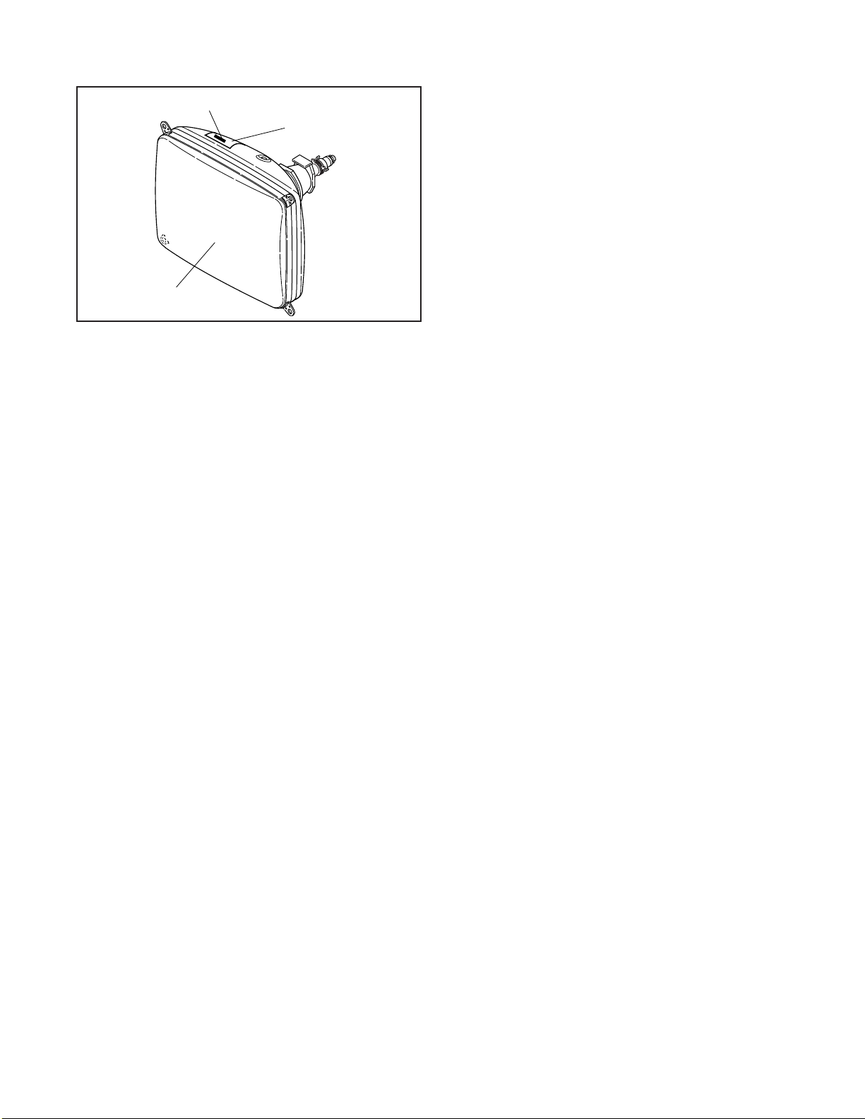
CRT Warning Label Location
CRT Type No.
CRT Warning
Label
CRT
20030408 12-2 L6605CA
Page 43
ELECTRICAL PARTS LIST
PRODUCT SAFETY NOTE: Products marked with a
# have special characteristics important to safety.
Before replacing any of these components, read carefully the product safety notice in this service manual.
Don't degrade the safety of the product through
improper servicing.
NOTES:
1. Parts that are not assigned part numbers (---------)
are not available.
2. Tolerance of Capacitors and Resistors are noted
with the following symbols.
C.....±0.25% D.....±0.5% F.....±1%
G.....±2% J......±5% K.....±10%
M.....±20% N.....±30% Z.....+80/-20%
MMA-393 CBA
Ref. No. Description Part No.
MMA-393 CBA 0ESA05083
Consists of the following
MAIN CBA --------------
CRT CBA --------------
MAIN CBA
Ref. No. Description Part No.
MAIN CBA
Consists of the following
CAPACITORS
C1 CERAMIC CAP.(AX) F Z 0.01µF/25V CDA1EZT0F103
C2 ELECTROLYTIC CAP. 100µF/10V M or CE1AMASTL101
ELECTROLYTIC CAP. 100µF/10V M CE1AMASDL101
C3 ELECTROLYTIC CAP. 4.7µF/50V M or CE1JMASTL4R7
ELECTROLYTIC CAP. 4.7µF/50V M CE1JMASDL4R7
C31 ELECTROLYTIC CAP. 100µF/10V M or CE1AMASTL101
ELECTROLYTIC CAP. 100µF/10V M CE1AMASDL101
C32 CERAMIC CAP.(AX) F Z 0.01µF/25V CDA1EZT0F103
C34 ELECTROLYTIC CAP. 0.47µF/50V M or CE1JMASTLR47
ELECTROLYTIC CAP. 0.47µF/50V M CE1JMASDLR47
C35 CERAMIC CAP.(AX) CH J 56pF/50V CA1J560TU008
C36 CERAMIC CAP.(AX) B K 100pF/50V CCA1JKT0B101
C37 CERAMIC CAP.(AX) F Z 0.1µF/50V or CA1J104TU014
CERAMIC CAP.(AX) F Z 0.1µF/50V CCA1JZT0F104
C38 ELECTROLYTIC CAP. 10µF/50V M or CE1JMASTL100
ELECTROLYTIC CAP. 10µF/50V M CE1JMASDL100
C41 ELECTROLYTIC CAP. 0.47µF/50V M or CE1JMASTLR47
ELECTROLYTIC CAP. 0.47µF/50V M CE1JMASDLR47
C51 CERAMIC CAP.(AX) B K 1000pF/50V CCA1JKT0B102
C52 CERAMIC CAP.(AX) F Z 0.01µF/25V CDA1EZT0F103
C53 ELECTROLYTIC CAP. 100µF/10V M or CE1AMASTL101
ELECTROLYTIC CAP. 100µF/10V M CE1AMASDL101
C54 CERAMIC CAP.(AX) B K 0.01µF/50V CA1J103TU011
C55 CERAMIC CAP.(AX) F Z 0.01µF/25V CDA1EZT0F103
C56 PCB JUMPER D0.6-P5.0 JW5.0T
------------
Ref. No. Description Part No.
C57 FILM CAP.(P) 0.047µF/50V J or CMA1JJS00473
FILM CAP.(P) 0.047µF/50V J CA1J473MS029
C58 FILM CAP.(P) 0.033µF/50V J or CMA1JJS00333
FILM CAP.(P) 0.033µF/50V J CA1J333MS029
C111 ELECTROLYTIC CAP. 47µF/16V M or CE1CMASTL470
ELECTROLYTIC CAP. 47µF/16V M CE1CMASDL470
C112 ELECTROLYTIC CAP. 4.7µF/50V M or CE1JMASTL4R7
ELECTROLYTIC CAP. 4.7µF/50V M CE1JMASDL4R7
C113 CERAMIC CAP.(AX) F Z 0.1µF/50V or CA1J104TU014
CERAMIC CAP.(AX) F Z 0.1µF/50V CCA1JZT0F104
C114 FILM CAP.(P) 0.001µF/50V J or CMA1JJS00102
FILM CAP.(P) 0.001µF/50V J CA1J102MS029
C115 ELECTROLYTIC CAP. 0.1µF/50V M or CE1JMASTLR10
ELECTROLYTIC CAP. 0.1µF/50V M or CE1JMASDLR10
ELECTROLYTIC CAP. 0.1µF/50V M CE1JMASDL0R1
C116 CERAMIC CAP.(AX) B K 220pF/50V CCA1JKT0B221
C117 CERAMIC CAP.(AX) Y K 0.01µF/16V CDA1CKT0Y103
C119 ELECTROLYTIC CAP. 100µF/10V M or CE1AMASTL101
ELECTROLYTIC CAP. 100µF/10V M CE1AMASDL101
C120 CERAMIC CAP.(AX) F Z 0.01µF/25V CDA1EZT0F103
C121 CERAMIC CAP.(AX) X K 1200pF/16V CDA1CKT0X122
C132 CERAMIC CAP.(AX) F Z 0.1µF/50V or CA1J104TU014
CERAMIC CAP.(AX) F Z 0.1µF/50V CCA1JZT0F104
C133 CERAMIC CAP.(AX) F Z 0.01µF/25V CDA1EZT0F103
C151 CERAMIC CAP.(AX) F Z 0.01µF/25V CDA1EZT0F103
C152 CERAMIC CAP.(AX) B K 220pF/50V CCA1JKT0B221
C153 CERAMIC CAP.(AX) B K 220pF/50V CCA1JKT0B221
C155 ELECTROLYTIC CAP. 47µF/16V M or CE1CMASTL470
ELECTROLYTIC CAP. 47µF/16V M CE1CMASDL470
C156 CERAMIC CAP.(AX) F Z 0.1µF/50V or CA1J104TU014
CERAMIC CAP.(AX) F Z 0.1µF/50V CCA1JZT0F104
C301 CERAMIC CAP.(AX) CH J 120pF/50V CA1J121TU008
C302 ELECTROLYTIC CAP. 1µF/50V M or CE1JMASTL1R0
ELECTROLYTIC CAP. 1µF/50V M or CE1JMASDL1R0
ELECTROLYTIC CAP. 1µF/50V M CE1JMASDL010
C303 CERAMIC CAP.(AX) B K 0.015µF/50V CA1J153TU011
C306 ELECTROLYTIC CAP. 100µF/10V M or CE1AMASTL101
ELECTROLYTIC CAP. 100µF/10V M CE1AMASDL101
C308 ELECTROLYTIC CAP. 0.47µF/50V M or CE1JMASTLR47
ELECTROLYTIC CAP. 0.47µF/50V M CE1JMASDLR47
C322 ELECTROLYTIC CAP. 0.47µF/50V M or CE1JMASTLR47
ELECTROLYTIC CAP. 0.47µF/50V M CE1JMASDLR47
C324 ELECTROLYTIC CAP. 10µF/50V M or CE1JMASTL100
ELECTROLYTIC CAP. 10µF/50V M CE1JMASDL100
C325 CERAMIC CAP.(AX) B K 220pF/50V CCA1JKT0B221
C328 ELECTROLYTIC CAP. 10µF/50V M or CE1JMASTL100
ELECTROLYTIC CAP. 10µF/50V M CE1JMASDL100
C329 CERAMIC CAP.(AX) F Z 0.01µF/25V CDA1EZT0F103
C330 STACKED FILM CAP. 0.47µF/50V J CMA1JJS00474
C341 CERAMIC CAP.(AX) B K 0.01µF/50V CA1J103TU011
C342 ELECTROLYTIC CAP. 1µF/50V M or CE1JMASTL1R0
ELECTROLYTIC CAP. 1µF/50V M or CE1JMASDL1R0
ELECTROLYTIC CAP. 1µF/50V M CE1JMASDL010
C343 CERAMIC CAP.(AX) B K 0.01µF/50V CA1J103TU011
C345 ELECTROLYTIC CAP. 2200µF/10V M CE1AMZNTL222
C347 ELECTROLYTIC CAP. 470µF/10V M or CE1AMASTL471
ELECTROLYTIC CAP. 470µF/10V M CE1AMASDL471
20030408 13-1 L6605EL
Page 44
Ref. No. Description Part No.
C349 ELECTROLYTIC CAP. 470µF/10V M or CE1AMASTL471
ELECTROLYTIC CAP. 470µF/10V M CE1AMASDL471
C353 ELECTROLYTIC CAP. 1µF/50V M or CE1JMASTL1R0
ELECTROLYTIC CAP. 1µF/50V M or CE1JMASDL1R0
ELECTROLYTIC CAP. 1µF/50V M CE1JMASDL010
C401 CERAMIC CAP.(AX) X K 4700pF/16V CDA1CKT0X472
C402 MYLAR CAP. 0.22µF/50V J or CMA1JJS00224
FILM CAP.(P) 0.22µF/50V J CA1J224MS029
C403 ELECTROLYTIC CAP. 1µF/50V M or CE1JMASTL1R0
ELECTROLYTIC CAP. 1µF/50V M or CE1JMASDL1R0
ELECTROLYTIC CAP. 1µF/50V M CE1JMASDL010
C404 ELECTROLYTIC CAP. 0.1µF/50V M or CE1JMASTLR10
ELECTROLYTIC CAP. 0.1µF/50V M or CE1JMASDLR10
ELECTROLYTIC CAP. 0.1µF/50V M CE1JMASDL0R1
C405 ELECTROLYTIC CAP. 47µF/16V M or CE1CMASTL470
ELECTROLYTIC CAP. 47µF/16V M CE1CMASDL470
C408 CERAMIC CAP.(AX) F Z 0.1µF/50V or CA1J104TU014
CERAMIC CAP.(AX) F Z 0.1µF/50V CCA1JZT0F104
C409 ELECTROLYTIC CAP. 1µF/50V M or CE1JMASTL1R0
ELECTROLYTIC CAP. 1µF/50V M or CE1JMASDL1R0
ELECTROLYTIC CAP. 1µF/50V M CE1JMASDL010
C421 CERAMIC CAP.(AX) X K 4700pF/16V CDA1CKT0X472
C422 CERAMIC CAP.(AX) X K 4700pF/16V CDA1CKT0X472
C423 PCB JUMPER D0.6-P5.0 JW5.0T
C424 PCB JUMPER D0.6-P5.0 JW5.0T
C431 ELECTROLYTIC CAP. 2.2µF/50V M or CE1JMASTL2R2
ELECTROLYTIC CAP. 2.2µF/50V M CE1JMASDL2R2
C432 ELECTROLYTIC CAP. 10µF/50V M or CE1JMASTL100
ELECTROLYTIC CAP. 10µF/50V M CE1JMASDL100
C433 CERAMIC CAP.(AX) X K 2700pF/16V CDA1CKT0X272
C434 FILM CAP.(P) 0.1µF/50V J or CMA1JJS00104
FILM CAP.(P) 0.1µF/50V J CA1J104MS029
C435 CERAMIC CAP.(AX) F Z 0.01µF/25V CDA1EZT0F103
C441 CERAMIC CAP.(AX) F Z 0.01µF/25V CDA1EZT0F103
C442 ELECTROLYTIC CAP. 10µF/50V M or CE1JMASTL100
ELECTROLYTIC CAP. 10µF/50V M CE1JMASDL100
C446 ELECTROLYTIC CAP. 1µF/50V M or CE1JMASTL1R0
ELECTROLYTIC CAP. 1µF/50V M or CE1JMASDL1R0
ELECTROLYTIC CAP. 1µF/50V M CE1JMASDL010
C527# ELECTROLYTIC CAP. 3.3µF/50V M or CE1JMASTL3R3
# ELECTROLYTIC CAP. 3.3µF/50V M CE1JMASDL3R3
C531 ELECTROLYTIC CAP. 100µF/10V M or CE1AMASTL101
ELECTROLYTIC CAP. 100µF/10V M CE1AMASDL101
C532 ELECTROLYTIC CAP. 47µF/35V M or CE1GMASTL470
ELECTROLYTIC CAP. 47µF/35V M CE1GMASDL470
C533 FILM CAP.(P) 0.1µF/50V J or CMA1JJS00104
FILM CAP.(P) 0.1µF/50V J CA1J104MS029
C535 ELECTROLYTIC CAP. 1.5µF/50V M LL CE1JMASLL1R5
C539# ELECTROLYTIC CAP. 1000µF/25V M or CE1EMZNTL102
# ELECTROLYTIC CAP. 1000µF/25V M or CE1EMZPDL102
# ELECTROLYTIC CAP. 1000µF/25V M CE1EMZADL102
C541 ELECTROLYTIC CAP. 470µF/35V M(VR) or CE1GMZNTL471
ELECTROLYTIC CAP. 470µF/35V M or CE1GMZADL471
ELECTROLYTIC CAP. 470µF/35V M CE1GMZNDL471
C551 PCB JUMPER D0.6-P5.0 JW5.0T
C552# METALIZED PLYESTER CAP. 1µF/100V J CT2A105MS065
C556 FILM CAP.(P) 0.1µF/50V J or CMA1JJS00104
FILM CAP.(P) 0.1µF/50V J CA1J104MS029
C561 ELECTROLYTIC CAP. 47µF/35V M or CE1GMASTL470
ELECTROLYTIC CAP. 47µF/35V M CE1GMASDL470
C562 ELECTROLYTIC CAP. 470µF/25V M or CE1EMZNTL471
Ref. No. Description Part No.
ELECTROLYTIC CAP. 470µF/25V M or CE1EMZNDL471
ELECTROLYTIC CAP. 470µF/25V M CE1EMZADL471
C565 FILM CAP.(P) 0.1µF/50V J or CMA1JJS00104
FILM CAP.(P) 0.1µF/50V J CA1J104MS029
C567# PP CAP. 0.0033µF/1.6KV J or CA3C332VC010
# PP CAP. 0.0033µF/1.6KV J or CT3C332MS039
# PP CAP. 0.0033µF/1.6KV J or CBH3CJQ00332
# METALLIZED FILM CAP. 0.0033µF/1.6KV J CT3C332F7002
C568 CERAMIC CAP.(AX) B K 0.022µF/50V CA1J223TU011
C571# P. P. CA P 0 .3 3 µF/200V J or CA2D334VC012
# PP CAP. 0.33µF/250V J or CT2E334MS041
# METALLIZED FILM CAP. 0.33µF/200V J CT2D334F7001
C572 P.P. CAP 0.18µF/200V J or CA2D184VC012
PP CAP. 0.18µF/250V J or CT2E184MS041
METALLIZED FILM CAP. 0.18µF/200V J CT2D184F7001
C574# ELECTROLYTIC CAP. 10µF/250V M CE2EMASDL100
C577 ELECTROLYTIC CAP. 47µF/35V M or CE1GMASTL470
ELECTROLYTIC CAP. 47µF/35V M CE1GMASDL470
C578 FILM CAP.(P) 0.01µF/50V J or CMA1JJS00103
FILM CAP.(P) 0.01µF/50V J CA1J103MS029
C580# PP CAP. 0.015µF/1.6KV J or CA3C153VC010
# PP CAP. 0.015µF/1.6KV J or CT3C153MS039
# PP CAP. 0.015µF/1.6KV J CBH3CJQ00153
C582# P. P. CA P. 0 .0 2 2 µF/200V J or CA2D223VC013
# P. P. C AP. 0 . 02 2 µF/200V K or CBP2DKD00223
# METALLIZED FILM CAP. 0.022µF/200V J CT2D223F7002
C584# ELECTROLYTIC CAP. 1µF/160V M or CE2CMASTL1R0
# ELECTROLYTIC CAP. 1µF/160V M CE2CMASDL1R0
C585 CERAMIC CAP. B K 100pF/500V CCD2JKS0B101
C591 ELECTROLYTIC CAP. 10µF/50V M or CE1JMASTL100
ELECTROLYTIC CAP. 10µF/50V M CE1JMASDL100
C601# METALLIZED FILM CAP. 0.1µF/250V or CT2E104MS037
# FILM CAP.(MP) 0.1µF/250V K or CT2E104DC011
# METALLIZED FILM CAP. 0.1µF/275V K CT2E104HJE06
C603 CERAMIC CAP.(AX) B K 470pF/50V CCA1JKT0B471
C605 CERAMIC CAP. F Z 0.01µF/500V or CCD2JZP0F103
CERAMIC CAP. 0.01µF/AC250V CCD2EZA0F103
C606 CERAMIC CAP. F Z 0.01µF/500V or CCD2JZP0F103
CERAMIC CAP. 0.01µF/AC250V CCD2EZA0F103
C609 CERAMIC CAP. B K 1000pF/2KV or CCD3DKD0B102
CERAMIC CAP. B K 1000pF/2KV or CCD3DKP0B102
CERAMIC CAP. 1000pF/2KV CA3D102PAN04
C610# ELECTROLYTIC CAP. 470µF/200V or CA2D471NC013
# ELECTROLYTIC CAP. 470µF/200V M CE2DMZNDL471
C611 FILM CAP.(P) 0.0056µF/50V J or CMA1JJS00562
FILM CAP.(P) 0.0056µF/50V J CA1J562MS029
C613 FILM CAP.(P) 0.056µF/50V J or CMA1JJS00563
FILM CAP.(P) 0.056µF/50V J CA1J563MS029
C614 CERAMIC CAP.(AX) X K 2700pF/16V CDA1CKT0X272
C615 CERAMIC CAP.(AX) B K 100pF/50V CCA1JKT0B101
C616 FILM CAP.(P) 0.1µF/50V J or CMA1JJS00104
FILM CAP.(P) 0.1µF/50V J CA1J104MS029
C618 FILM CAP.(P) 0.1µF/50V J or CMA1JJS00104
FILM CAP.(P) 0.1µF/50V J CA1J104MS029
If C642 is 0.01µF, then C643 is 0.01µF.
C642# SAFETY CAP. 10000pF/250V or CCG2EMA0F103
# SAFETY CAP. F M 0.01µF/250V or CCG2EMP0F103
# CERAMIC CAP. 0.01µF F CS CCG2HMN0F103
C643# SAFETY CAP. 10000pF/250V or CCG2EMA0F103
# SAFETY CAP. F M 0.01µF/250V or CCG2EMP0F103
# CERAMIC CAP. 0.01µF F CS CCG2HMN0F103
20030408 13-2 L6605EL
Page 45
Ref. No. Description Part No.
If C643 is 4700pF, then JS642 (PCBJUMPER) is used.
C643# SAFETY CAP. 4700pF/250V KX CA2E472MR050
JS642 PCB JUMPER D0.6-P10.0 JW10.0T
C654# ELECTROLYTIC CAP. 1µF/50V M or CE1JMASTL1R0
# ELECTROLYTIC CAP. 1µF/50V M or CE1JMASDL1R0
# ELECTROLYTIC CAP. 1µF/50V M CE1JMASDL010
C655 ELECTROLYTIC CAP. 1000µF/16V M(VR/HC) or CE1CMZNTL102
ELECTROLYTIC CAP. 1000µF/16V M or CE1CMZPDL102
ELECTROLYTIC CAP. 1000µF/16V M CE1CMZADL102
C656 ELECTROLYTIC CAP. 100µF/160V M or CE2CMZPTL101
ELECTROLYTIC CAP. 100µF/160V M CE2CMZNDL101
C657 ELECTROLYTIC CAP. 470µF/35V M(VR) or CE1GMZNTL471
ELECTROLYTIC CAP. 470µF/35V M or CE1GMZADL471
ELECTROLYTIC CAP. 470µF/35V M CE1GMZNDL471
C658# ELECTROLYTIC CAP. 1000µF/16V M(VR/HC) or CE1CMZNTL102
# ELECTROLYTIC CAP. 1000µF/16V M or CE1CMZPDL102
# ELECTROLYTIC CAP. 1000µF/16V M CE1CMZADL102
C667 ELECTROLYTIC CAP. 1µF/50V M or CE1JMASTL1R0
ELECTROLYTIC CAP. 1µF/50V M or CE1JMASDL1R0
ELECTROLYTIC CAP. 1µF/50V M CE1JMASDL010
C681 ELECTROLYTIC CAP. 100µF/10V M or CE1AMASTL101
ELECTROLYTIC CAP. 100µF/10V M CE1AMASDL101
C682 ELECTROLYTIC CAP. 100µF/10V M or CE1AMASTL101
ELECTROLYTIC CAP. 100µF/10V M CE1AMASDL101
C683 ELECTROLYTIC CAP. 100µF/10V M or CE1AMASTL101
ELECTROLYTIC CAP. 100µF/10V M CE1AMASDL101
C686 ELECTROLYTIC CAP. 33µF/16V M or CE1CMASTL330
ELECTROLYTIC CAP. 33µF/16V M CE1CMASDL330
C687 ELECTROLYTIC CAP. 100µF/10V M or CE1AMASTL101
ELECTROLYTIC CAP. 100µF/10V M CE1AMASDL101
C692 ELECTROLYTIC CAP. 100µF/160V M or CE2CMZPTL101
ELECTROLYTIC CAP. 100µF/160V M CE2CMZNDL101
C701 CERAMIC CAP.(AX) B K 100pF/50V CCA1JKT0B101
C711 CERAMIC CAP.(AX) X K 4700pF/16V CDA1CKT0X472
C712 ELECTROLYTIC CAP. 0.47µF/50V M or CE1JMASTLR47
ELECTROLYTIC CAP. 0.47µF/50V M CE1JMASDLR47
C721 CERAMIC CAP.(AX) X K 4700pF/16V CDA1CKT0X472
C722 ELECTROLYTIC CAP. 0.47µF/50V M or CE1JMASTLR47
ELECTROLYTIC CAP. 0.47µF/50V M CE1JMASDLR47
C801 ELECTROLYTIC CAP. 470µF/16V M or CE1CMASTL471
ELECTROLYTIC CAP. 470µF/16V M CE1CMASDL471
C802 ELECTROLYTIC CAP. 470µF/16V M or CE1CMASTL471
ELECTROLYTIC CAP. 470µF/16V M CE1CMASDL471
C803 FILM CAP.(P) 0.1µF/50V J or CMA1JJS00104
FILM CAP.(P) 0.1µF/50V J CA1J104MS029
C804 FILM CAP.(P) 0.1µF/50V J or CMA1JJS00104
FILM CAP.(P) 0.1µF/50V J CA1J104MS029
C808 ELECTROLYTIC CAP. 1µF/50V M or CE1JMASTL1R0
ELECTROLYTIC CAP. 1µF/50V M or CE1JMASDL1R0
ELECTROLYTIC CAP. 1µF/50V M CE1JMASDL010
C809 ELECTROLYTIC CAP. 1µF/50V M or CE1JMASTL1R0
ELECTROLYTIC CAP. 1µF/50V M or CE1JMASDL1R0
ELECTROLYTIC CAP. 1µF/50V M CE1JMASDL010
C812 ELECTROLYTIC CAP. 22µF/16V M or CE1CMASTL220
ELECTROLYTIC CAP. 22µF/16V M CE1CMASDL220
C814 ELECTROLYTIC CAP. 100µF/16V M or CE1CMASTL101
ELECTROLYTIC CAP. 100µF/16V M CE1CMASDL101
C821 ELECTROLYTIC CAP. 470µF/16V M or CE1CMASTL471
ELECTROLYTIC CAP. 470µF/16V M CE1CMASDL471
C822 ELECTROLYTIC CAP. 470µF/16V M or CE1CMASTL471
ELECTROLYTIC CAP. 470µF/16V M CE1CMASDL471
Ref. No. Description Part No.
C827# ELECTROLYTIC CAP. 100µF/16V M or CE1CMASTL101
# ELECTROLYTIC CAP. 100µF/16V M CE1CMASDL101
C831 ELECTROLYTIC CAP. 100µF/16V M or CE1CMASTL101
ELECTROLYTIC CAP. 100µF/16V M CE1CMASDL101
C833 CERAMIC CAP.(AX) F Z 0.01µF/25V CDA1EZT0F103
CONNECTORS
CN571# CONNECTOR BASE, 5P TV-50P-05-V3 or J3TVC05TG002
# CONNECTOR BASE, 5P RTB-1.5-5P or J3RTC05JG001
# CONNECTOR BASE, 5P W-P3005-02 1730812
CN691# CONNECTOR BASE, 2P TV-50P-02-V3 or J3TVC02TG002
# CONNECTOR BASE, 2P RTB-1.5-2P J3RTC02JG001
CN801 STRAIGHT CONNECTOR BASE 00 8283 0212 00
CN802 STRAIGHT CONNECTOR BASE 00 8283 0212 00
000 or
STRAIGHT PIN HEADER, 2P 173981-2 1770258
000 or
STRAIGHT PIN HEADER, 2P 173981-2 1770258
J383C02UG002
J383C02UG002
DIODES
D101 SWITCHING DIODE 1SS133(T-77) or QDTZ001SS133
SWITCHING DIODE 1N4148 NDTZ001N4148
D102 SWITCHING DIODE 1SS133(T-77) or QDTZ001SS133
SWITCHING DIODE 1N4148 NDTZ001N4148
D131 ZENER DIODE MTZJT-775.1B or QDTB0MTZJ5R1
ZENER DIODE DZ-5.1BSBT265 NDTB0DZ5R1BS
D151 ZENER DIODE MTZJT-775.6B or QDTB0MTZJ5R6
ZENER DIODE DZ-5.6BSBT265 NDTB0DZ5R6BS
D181 SWITCHING DIODE 1SS133(T-77) or QDTZ001SS133
SWITCHING DIODE 1N4148 NDTZ001N4148
D322 SWITCHING DIODE 1SS133(T-77) or QDTZ001SS133
SWITCHING DIODE 1N4148 NDTZ001N4148
D323 ZENER DIODE MTZJT-7710B or QDTB00MTZJ10
ZENER DIODE DZ-10BSBT265 NDTB00DZ10BS
D326 SWITCHING DIODE 1SS133(T-77) or QDTZ001SS133
SWITCHING DIODE 1N4148 NDTZ001N4148
D327 ZENER DIODE MTZJT-778.2B or QDTB0MTZJ8R2
ZENER DIODE DZ-8.2BSBT265 NDTB0DZ8R2BS
D351 SWITCHING DIODE 1SS133(T-77) or QDTZ001SS133
SWITCHING DIODE 1N4148 NDTZ001N4148
D352 SWITCHING DIODE 1SS133(T-77) or QDTZ001SS133
SWITCHING DIODE 1N4148 NDTZ001N4148
D353 SWITCHING DIODE 1SS133(T-77) or QDTZ001SS133
SWITCHING DIODE 1N4148 NDTZ001N4148
D525# ZENER DIODE MTZJT-7720B or QDTB00MTZJ20
# ZENER DIODE DZ-20BSBT265 NDTB00DZ20BS
D526# SWITCHING DIODE 1SS133(T-77) or QDTZ001SS133
# SWITCHING DIODE 1N4148 NDTZ001N4148
D532 DIODE 1N5397-B or NDLZ001N5397
RECTIFIER DIODE ERA15-02 AERA1502****
D552# ZENER DIODE MTZJT-7715B or QDTB00MTZJ15
# ZENER DIODE DZ-15BSBT265 NDTB00DZ15BS
D558 SWITCHING DIODE 1SS133(T-77) or QDTZ001SS133
SWITCHING DIODE 1N4148 NDTZ001N4148
D571# DIODE FR104-B or NDLZ000FR104
# RECTIFIER DIODE ERA22-02 or QDPZ0ERA2202
# RECTIFIER DIODE 10ELS2 QDQZ0010ELS2
D572# RECTIFIER DIODE ERA22-02 or QDPZ0ERA2202
# RECTIFIER DIODE 10ELS2 QDQZ0010ELS2
D573# RECTIFIER DIODE ERA22-02 or QDPZ0ERA2202
# RECTIFIER DIODE 10ELS2 QDQZ0010ELS2
D580 DIODE ERD07-15 QDLZ0ERD0715
D582 FAST RECOVERY DIODE ERD38-06 QDQZ0ERD3806
20030408 13-3 L6605EL
Page 46
Ref. No. Description Part No.
D583 SWITCHING DIODE 1SS133(T-77) or QDTZ001SS133
SWITCHING DIODE 1N4148 NDTZ001N4148
D584# SWITCHING DIODE 1SS133(T-77) or QDTZ001SS133
# SWITCHING DIODE 1N4148 NDTZ001N4148
D585 SWITCHING DIODE 1SS133(T-77) or QDTZ001SS133
SWITCHING DIODE 1N4148 NDTZ001N4148
D586 SWITCHING DIODE 1SS133(T-77) or QDTZ001SS133
SWITCHING DIODE 1N4148 NDTZ001N4148
D587 ZENER DIODE MTZJT-776.8B or QDTB0MTZJ6R8
ZENER DIODE DZ-6.8BSBT265 NDTB0DZ6R8BS
D588 SWITCHING DIODE 1SS133(T-77) or QDTZ001SS133
SWITCHING DIODE 1N4148 NDTZ001N4148
D591# ZENER DIODE MTZJT-7736B or QDTB00MTZJ36
# ZENER DIODE DZ-36BSBT265 NDTB00DZ36BS
D595# SWITCHING DIODE 1SS133(T-77) or QDTZ001SS133
# SWITCHING DIODE 1N4148 NDTZ001N4148
D597 ZENER DIODE MTZJT-776.8B or QDTB0MTZJ6R8
ZENER DIODE DZ-6.8BSBT265 NDTB0DZ6R8BS
D605# DIODE 1N5406 or NDLZ001N5406
# DIODE ERC04-06L3 QD4Z0ERC0406
D606# DIODE 1N5406 or NDLZ001N5406
# DIODE ERC04-06L3 QD4Z0ERC0406
D607# DIODE 1N5406 or NDLZ001N5406
# DIODE ERC04-06L3 QD4Z0ERC0406
D608# DIODE 1N5406 or NDLZ001N5406
# DIODE ERC04-06L3 QD4Z0ERC0406
D609 SWITCHING DIODE 1SS133(T-77) or QDTZ001SS133
SWITCHING DIODE 1N4148 NDTZ001N4148
D611# ZENER DIODE MTZJT-7715B or QDTB00MTZJ15
# ZENER DIODE DZ-15BSBT265 NDTB00DZ15BS
D615# SWITCHING DIODE 1N4148 T-77 QDTZ001N4148
D621 ZENER DIODE MTZJT-777.5B or QDTB0MTZJ7R5
ZENER DIODE DZ-7.5BSBT265 NDTB0DZ7R5BS
D622 SWITCHING DIODE 1SS133(T-77) or QDTZ001SS133
SWITCHING DIODE 1N4148 NDTZ001N4148
D641 SWITCHING DIODE 1SS133(T-77) or QDTZ001SS133
SWITCHING DIODE 1N4148 NDTZ001N4148
D642# SWITCHING DIODE 1SS133(T-77) or QDTZ001SS133
# SWITCHING DIODE 1N4148 NDTZ001N4148
D651# FAST RECOVERY DIODE 30DF6 or QDWZ00030DF6
# DIODE ERD29-06J or QD4Z0ERD2906
# FAST RECOVERY DIODE FE201-6 QDLZ00FE2016
D652# DIODE FR154 or NDLZ000FR154
# FAST RECOVERY DIODE ERB44-02 QDPZ0ERB4402
D653 DIODE FR154 or NDLZ000FR154
FAST RECOVERY DIODE ERB44-02 QDPZ0ERB4402
D654# SWITCHING DIODE 1SS133(T-77) or QDTZ001SS133
# SWITCHING DIODE 1N4148 NDTZ001N4148
D655# DIODE FR154 or NDLZ000FR154
# FAST RECOVERY DIODE ERB44-02 QDPZ0ERB4402
D657# DIODE 1ZC36 QDQZ0001ZC36
D660 SWITCHING DIODE 1SS133(T-77) or QDTZ001SS133
SWITCHING DIODE 1N4148 NDTZ001N4148
D661# SWITCHING DIODE 1SS133(T-77) or QDTZ001SS133
# SWITCHING DIODE 1N4148 NDTZ001N4148
D662# ZENER DIODE MTZJT-776.8B or QDTB0MTZJ6R8
# ZENER DIODE DZ-6.8BSBT265 NDTB0DZ6R8BS
D666 ZENER DIODE MTZJT-7736B or QDTB00MTZJ36
ZENER DIODE DZ-36BSBT265 NDTB00DZ36BS
D671# SWITCHING DIODE 1SS133(T-77) or QDTZ001SS133
# SWITCHING DIODE 1N4148 NDTZ001N4148
Ref. No. Description Part No.
D672 PCB JUMPER D0.6-P5.0 JW5.0T
D673 SWITCHING DIODE 1SS133(T-77) or QDTZ001SS133
SWITCHING DIODE 1N4148 NDTZ001N4148
D681 ZENER DIODE MTZJT-779.1B or QDTB0MTZJ9R1
ZENER DIODE DZ-9.1BSBT265 NDTB0DZ9R1BS
D683 SCHOTTKY BARRIER DIODE ERA81-004 QDPZERA81004
D691# SWITCHING DIODE 1SS133(T-77) or QDTZ001SS133
# SWITCHING DIODE 1N4148 NDTZ001N4148
D695 ZENER DIODE MTZJT-778.2B or QDTB0MTZJ8R2
ZENER DIODE DZ-8.2BSBT265 NDTB0DZ8R2BS
D696 SWITCHING DIODE 1SS133(T-77) or QDTZ001SS133
SWITCHING DIODE 1N4148 NDTZ001N4148
D826 SWITCHING DIODE 1SS133(T-77) or QDTZ001SS133
SWITCHING DIODE 1N4148 NDTZ001N4148
D838 ZENER DIODE MTZJT-7710B or QDTB00MTZJ10
ZENER DIODE DZ-10BSBT265 NDTB00DZ10BS
D841# SWITCHING DIODE 1SS133(T-77) or QDTZ001SS133
# SWITCHING DIODE 1N4148 NDTZ001N4148
D842# ZENER DIODE MTZJT-775.1B or QDTB0MTZJ5R1
# ZENER DIODE DZ-5.1BSBT265 NDTB0DZ5R1BS
D845# SWITCHING DIODE 1SS133(T-77) or QDTZ001SS133
# SWITCHING DIODE 1N4148 NDTZ001N4148
ICS
IC31 IC:VIF/SIF DETECTOR M61111FP QSZBA0SMB010
IC111# IC M61271M8-050FP-61 QSZAB0RMB127
IC151 IC:MEMORY S524C20D21 or NSZBA0SSM028
IC:MEMORY AT24C02N-10SC or NSMMA0SAZ012
IC(EEPROM) M24C02-MN6 or NSMMA0SSS028
IC:MEMORY BR24C02F-W or QSMBA0SRM003
IC:MEMORY BR24C02F or QSMMA0SRM003
IC:EEPROM CAT24WC02JI or NSZBA0SBG001
IC(EEP-ROM) M24C02-WMN6 NSZAA0SSS004
IC401 IC:USA STEREO DECODER LA7765 QSZBA0SSY003
IC481 IC:SWITCHING TC4052BF(EL) or QSZBA0TTS096
IC:SWITCHING CD4052BCSJX NSZBA0TF3079
IC551# IC:VERTICAL OUTPUT LA78041 or QSZBA0SSY006
# IC:VERTICAL OUTPUT LA78045 QSZBA0SSY004
IC601# PHOTOCOUPLER PS2501-1W or QPEW0PS25011
# PHOTO COUPLER PS2501-1L or QPEL0PS25011
# PHOTOCOUPLER LTV-817B-F or NPEB0LTV817F
# PHOTOCOUPLER LTV-817C-F NPEC0LTV817F
IC802 AUDIO POWER IC AN17805A QSZBA0SMS007
COILS
L1 PCB JUMPER D0.6-P5.0 JW5.0T
L3 INDUCTOR 22µH-K-5FT or LLARKBSTU220
INDUCTOR 22µH-K LLARKDQKA220
L32 INDUCTOR 15µH-J-26T or LLAXJATTU150
INDUCTOR 15µH-K-26T LLAXKDTKA150
L33 INDUCTOR 22µH-J-26T or LLAXJATTU220
INDUCTOR 22µH-K-26T LLAXKDTKA220
L51 INDUCTOR 100µH-K-5FT or LLARKBSTU101
INDUCTOR 100µH-K LLARKDQKA101
L111 INDUCTOR 22µH-K-5FT or LLARKBSTU220
INDUCTOR 22µH-K LLARKDQKA220
L301 INDUCTOR 100µH-K-5FT or LLARKBSTU101
INDUCTOR 100µH-K LLARKDQKA101
L341 PCB JUMPER D0.6-P5.0 JW5.0T
L342 PCB JUMPER D0.6-P5.0 JW5.0T
L561 LINEARITY COIL ELH5L6136N LLBD00PMS008
L562 LINEARITY COIL ST02LN or LLBD00ZY2003
20030408 13-4 L6605EL
Page 47
Ref. No. Description Part No.
CHOKE COIL ELC13B102L or LLC102KMS001
CHOKE COIL CSA-LF048 LLBD00ZSA003
L601# LINE FILTER JLB2808 or LLBG00ZXB004
# LINE FILTER MS036 or LLBG00ZY2009
# LINE FILTER CSA-LF032 LLBG00ZSA007
L692 CHOKE COIL 47µH-K or LLBD00PKV007
POT COIL 47µH K or LLBD**DMM001
POT COIL 47µH K LLBD00DQE001
TRANSISTORS
Q31 TRANSISTOR 2SC2785(F) or QQSF02SC2785
TRANSISTOR 2SC2785(H) or QQSH02SC2785
TRANSISTOR 2SC2785(J) or QQSJ02SC2785
TRANSISTOR KTC3199(GR) or NQS10KTC3199
TRANSISTOR KTC3198(GR) or NQS40KTC3198
TRANSISTOR 2SC3331(T)-AANP or 2SC3331TZ
TRANSISTOR 2SC3331(U)-AANP or 2SC3331UZ
TRANSISTOR 2SC1815-GR(TPE2) QQS102SC1815
Q111 TRANSISTOR 2SC2785(F) or QQSF02SC2785
TRANSISTOR 2SC2785(H) or QQSH02SC2785
TRANSISTOR 2SC2785(J) or QQSJ02SC2785
TRANSISTOR KTC3199(GR) or NQS10KTC3199
TRANSISTOR KTC3198(GR) or NQS40KTC3198
TRANSISTOR 2SC3331(T)-AANP or 2SC3331TZ
TRANSISTOR 2SC3331(U)-AANP or 2SC3331UZ
TRANSISTOR 2SC1815-GR(TPE2) QQS102SC1815
Q321# TRANSISTOR 2SC2785(F) or QQSF02SC2785
# TRANSISTOR 2SC2785(H) or QQSH02SC2785
# TRANSISTOR 2SC2785(J) or QQSJ02SC2785
# TRANSISTOR KTC3199(GR) or NQS10KTC3199
# TRANSISTOR KTC3198(GR) or NQS40KTC3198
# TRANSISTOR 2SC3331(T)-AANP or 2SC3331TZ
# TRANSISTOR 2SC3331(U)-AANP or 2SC3331UZ
# TRANSISTOR 2SC1815-GR(TPE2) QQS102SC1815
Q411 TRANSISTOR 2SA1175(F) or QQSF02SA1175
TRANSISTOR KTA1267(GR) or NQS10KTA1267
TRANSISTOR KTA1266(GR) or NQS40KTA1266
TRANSISTOR 2SA1318(T)-AANP or 2SA1318TZ
TRANSISTOR 2SA1318(U)-AANP or 2SA1318UZ
TRANSISTOR 2SA1015-GR(TPE2) QQS102SA1015
Q441 TRANSISTOR 2SA1175(F) or QQSF02SA1175
TRANSISTOR KTA1267(GR) or NQS10KTA1267
TRANSISTOR KTA1266(GR) or NQS40KTA1266
TRANSISTOR 2SA1318(T)-AANP or 2SA1318TZ
TRANSISTOR 2SA1318(U)-AANP or 2SA1318UZ
TRANSISTOR 2SA1015-GR(TPE2) QQS102SA1015
Q481 TRANSISTOR 2SC2785(F) or QQSF02SC2785
TRANSISTOR 2SC2785(H) or QQSH02SC2785
TRANSISTOR 2SC2785(J) or QQSJ02SC2785
TRANSISTOR KTC3199(GR) or NQS10KTC3199
TRANSISTOR KTC3198(GR) or NQS40KTC3198
TRANSISTOR 2SC3331(T)-AANP or 2SC3331TZ
TRANSISTOR 2SC3331(U)-AANP or 2SC3331UZ
TRANSISTOR 2SC1815-GR(TPE2) QQS102SC1815
Q531 TRANSISTOR 2SC2785(F) or QQSF02SC2785
TRANSISTOR 2SC2785(H) or QQSH02SC2785
TRANSISTOR 2SC2785(J) or QQSJ02SC2785
TRANSISTOR KTC3199(GR) or NQS10KTC3199
TRANSISTOR KTC3198(GR) or NQS40KTC3198
TRANSISTOR 2SC3331(T)-AANP or 2SC3331TZ
TRANSISTOR 2SC3331(U)-AANP or 2SC3331UZ
Ref. No. Description Part No.
TRANSISTOR 2SC1815-GR(TPE2) QQS102SC1815
Q532 TRANSISTOR 2SC2785(F) or QQSF02SC2785
TRANSISTOR 2SC2785(H) or QQSH02SC2785
TRANSISTOR 2SC2785(J) or QQSJ02SC2785
TRANSISTOR KTC3199(GR) or NQS10KTC3199
TRANSISTOR KTC3198(GR) or NQS40KTC3198
TRANSISTOR 2SC3331(T)-AANP or 2SC3331TZ
TRANSISTOR 2SC3331(U)-AANP or 2SC3331UZ
TRANSISTOR 2SC1815-GR(TPE2) QQS102SC1815
Q551# TRANSISTOR 2SA1175(F) or QQSF02SA1175
# TRANSISTOR KTA1267(GR) or NQS10KTA1267
# TRANSISTOR KTA1266(GR) or NQS40KTA1266
# TRANSISTOR 2SA1318(T)-AANP or 2SA1318TZ
# TRANSISTOR 2SA1318(U)-AANP or 2SA1318UZ
# TRANSISTOR 2SA1015-GR(TPE2) QQS102SA1015
Q552# TRANSISTOR 2SD1666R or QQER02SD1666
# TRANSISTOR 2SD1666S or QQES02SD1666
# TRANSISTOR KTD2059(O) or NQ400KTD2059
# TRANSISTOR KTD2059(Y) or NQ4Y0KTD2059
# TRANSISTOR 2SD1825 Q2SD1825****
Q553 TRANSISTOR 2SC2785(F) or QQSF02SC2785
TRANSISTOR 2SC2785(H) or QQSH02SC2785
TRANSISTOR 2SC2785(J) or QQSJ02SC2785
TRANSISTOR KTC3199(GR) or NQS10KTC3199
TRANSISTOR KTC3198(GR) or NQS40KTC3198
TRANSISTOR 2SC3331(T)-AANP or 2SC3331TZ
TRANSISTOR 2SC3331(U)-AANP or 2SC3331UZ
TRANSISTOR 2SC1815-GR(TPE2) QQS102SC1815
Q561 TRANSISTOR 2SC2785(F) or QQSF02SC2785
TRANSISTOR 2SC2785(H) or QQSH02SC2785
TRANSISTOR 2SC2785(J) or QQSJ02SC2785
TRANSISTOR KTC3199(GR) or NQS10KTC3199
TRANSISTOR KTC3198(GR) or NQS40KTC3198
TRANSISTOR 2SC3331(T)-AANP or 2SC3331TZ
TRANSISTOR 2SC3331(U)-AANP or 2SC3331UZ
TRANSISTOR 2SC1815-GR(TPE2) QQS102SC1815
Q571# TRANSISTOR 2SD2634 or QQZZ02SD2634
# TRANSISTOR TT2142 QQZZ00TT2142
Q572 TRANSISTOR 2SC1627Y-TPE2 QQSY02SC1627
Q601# FET 2SK3407 QFFZ02SK3407
Q602# TRANSISTOR 2SC2120-O-TPE2 or QQS002SC2120
# TRANSISTOR 2SC2120-Y(TPE2) QQSY02SC2120
Q641 TRANSISTOR 2SA1175(F) or QQSF02SA1175
TRANSISTOR KTA1267(GR) or NQS10KTA1267
TRANSISTOR KTA1266(GR) or NQS40KTA1266
TRANSISTOR 2SA1318(T)-AANP or 2SA1318TZ
TRANSISTOR 2SA1318(U)-AANP or 2SA1318UZ
TRANSISTOR 2SA1015-GR(TPE2) QQS102SA1015
Q662# TRANSISTOR 2SC2785(F) or QQSF02SC2785
# TRANSISTOR 2SC2785(H) or QQSH02SC2785
# TRANSISTOR 2SC2785(J) or QQSJ02SC2785
# TRANSISTOR KTC3199(GR) or NQS10KTC3199
# TRANSISTOR KTC3198(GR) or NQS40KTC3198
# TRANSISTOR 2SC3331(T)-AANP or 2SC3331TZ
# TRANSISTOR 2SC3331(U)-AANP or 2SC3331UZ
# TRANSISTOR 2SC1815-GR(TPE2) QQS102SC1815
Q671# TRANSISTOR 2SA1175(F) or QQSF02SA1175
# TRANSISTOR KTA1267(GR) or NQS10KTA1267
# TRANSISTOR KTA1266(GR) or NQS40KTA1266
# TRANSISTOR 2SA1318(T)-AANP or 2SA1318TZ
# TRANSISTOR 2SA1318(U)-AANP or 2SA1318UZ
20030408 13-5 L6605EL
Page 48
Ref. No. Description Part No.
# TRANSISTOR 2SA1015-GR(TPE2) QQS102SA1015
Q675 TRANSISTOR 2SC2785(F) or QQSF02SC2785
TRANSISTOR 2SC2785(H) or QQSH02SC2785
TRANSISTOR 2SC2785(J) or QQSJ02SC2785
TRANSISTOR KTC3199(GR) or NQS10KTC3199
TRANSISTOR KTC3198(GR) or NQS40KTC3198
TRANSISTOR 2SC3331(T)-AANP or 2SC3331TZ
TRANSISTOR 2SC3331(U)-AANP or 2SC3331UZ
TRANSISTOR 2SC1815-GR(TPE2) QQS102SC1815
Q676 TRANSISTOR 2SC2785(F) or QQSF02SC2785
TRANSISTOR 2SC2785(H) or QQSH02SC2785
TRANSISTOR 2SC2785(J) or QQSJ02SC2785
TRANSISTOR KTC3199(GR) or NQS10KTC3199
TRANSISTOR KTC3198(GR) or NQS40KTC3198
TRANSISTOR 2SC3331(T)-AANP or 2SC3331TZ
TRANSISTOR 2SC3331(U)-AANP or 2SC3331UZ
TRANSISTOR 2SC1815-GR(TPE2) QQS102SC1815
Q681 TRANSISTOR 2SC2120-O-TPE2 or QQS002SC2120
TRANSISTOR 2SC2120-Y(TPE2) or QQSY02SC2120
TRANSISTOR KTC3203(Y) NQSY0KTC3203
Q682 TRANSISTOR 2SC2120-O-TPE2 or QQS002SC2120
TRANSISTOR 2SC2120-Y(TPE2) or QQSY02SC2120
TRANSISTOR KTC3203(Y) NQSY0KTC3203
Q683 TRANSISTOR 2SC2120-O-TPE2 or QQS002SC2120
TRANSISTOR 2SC2120-Y(TPE2) or QQSY02SC2120
TRANSISTOR KTC3203(Y) NQSY0KTC3203
Q696 RES. BUILT-IN TRANSISTOR BA1F4M-T or QQSZ00BA1F4M
RES. BUILT-IN TRANSISTOR KRC103M NQSZ0KRC103M
Q825 TRANSISTOR 2SC2785(F) or QQSF02SC2785
TRANSISTOR 2SC2785(H) or QQSH02SC2785
TRANSISTOR 2SC2785(J) or QQSJ02SC2785
TRANSISTOR KTC3199(GR) or NQS10KTC3199
TRANSISTOR KTC3198(GR) or NQS40KTC3198
TRANSISTOR 2SC3331(T)-AANP or 2SC3331TZ
TRANSISTOR 2SC3331(U)-AANP or 2SC3331UZ
TRANSISTOR 2SC1815-GR(TPE2) QQS102SC1815
Q831# TRANSISTOR 2SB892(S) or QQSS002SB892
# TRANSISTOR 2SB892(T) QQST002SB892
Q832 TRANSISTOR 2SC2785(F) or QQSF02SC2785
TRANSISTOR 2SC2785(H) or QQSH02SC2785
TRANSISTOR 2SC2785(J) or QQSJ02SC2785
TRANSISTOR KTC3199(GR) or NQS10KTC3199
TRANSISTOR KTC3198(GR) or NQS40KTC3198
TRANSISTOR 2SC3331(T)-AANP or 2SC3331TZ
TRANSISTOR 2SC3331(U)-AANP or 2SC3331UZ
TRANSISTOR 2SC1815-GR(TPE2) QQS102SC1815
Q833# TRANSISTOR 2SC2785(F) or QQSF02SC2785
# TRANSISTOR 2SC2785(H) or QQSH02SC2785
# TRANSISTOR 2SC2785(J) or QQSJ02SC2785
# TRANSISTOR KTC3199(GR) or NQS10KTC3199
# TRANSISTOR KTC3198(GR) or NQS40KTC3198
# TRANSISTOR 2SC3331(T)-AANP or 2SC3331TZ
# TRANSISTOR 2SC3331(U)-AANP or 2SC3331UZ
# TRANSISTOR 2SC1815-GR(TPE2) QQS102SC1815
RESISTORS
R3 PCB JUMPER D0.6-P5.0 JW5.0T
R4 CARBON RES. 1/4W J 100 Ω or RCX4JATZ0101
CARBON RES. 1/6W J 100 Ω RCX6JATZ0101
R5 CARBON RES. 1/4W J 100 Ω or RCX4JATZ0101
CARBON RES. 1/6W J 100 Ω RCX6JATZ0101
Ref. No. Description Part No.
R21 CARBON RES. 1/4W J 6.8k Ω RCX4JATZ0682
R31 CARBON RES. 1/4W J 2.2k Ω RCX4JATZ0222
R32 CARBON RES. 1/4W J 390 Ω or RCX4JATZ0391
CARBON RES. 1/6W J 390 Ω RCX6JATZ0391
R33 CARBON RES. 1/4W J 270 Ω or RCX4JATZ0271
CARBON RES. 1/6W J 270 Ω RCX6JATZ0271
R34 CARBON RES. 1/4W J 180 Ω or RCX4JATZ0181
CARBON RES. 1/6W J 180 Ω RCX6JATZ0181
R36 CARBON RES. 1/4W J 10k Ω RCX4JATZ0103
R37 CARBON RES. 1/4W J 470 Ω or RCX4JATZ0471
CARBON RES. 1/6W J 470 Ω RCX6JATZ0471
R41 CARBON RES. 1/4W J 2.2k Ω RCX4JATZ0222
R42 CARBON RES. 1/4W J 56k Ω RCX4JATZ0563
R43 CARBON RES. 1/4W J 12k Ω RCX4JATZ0123
R51 CARBON RES. 1/4W J 220k Ω RCX4JATZ0224
R52 CARBON RES. 1/4W J 220k Ω RCX4JATZ0224
R54 CARBON RES. 1/4W J 22k Ω RCX4JATZ0223
R102 CARBON RES. 1/4W J 2.2k Ω RCX4JATZ0222
R103 CARBON RES. 1/4W J 1.8k Ω RCX4JATZ0182
R104 CARBON RES. 1/4W J 3.3k Ω RCX4JATZ0332
R105 CARBON RES. 1/4W J 4.7k Ω RCX4JATZ0472
R106 CARBON RES. 1/4W J 8.2k Ω RCX4JATZ0822
R111# CARBON RES. 1/4W J 100 Ω or RCX4JATZ0101
# CARBON RES. 1/6W J 100 Ω RCX6JATZ0101
R112 CARBON RES. 1/4W J 10k Ω RCX4JATZ0103
R113 CARBON RES. 1/4W J 470k Ω RCX4JATZ0474
R114 CARBON RES. 1/4W J 1k Ω or RCX4JATZ0102
CARBON RES. 1/6W J 1k Ω RCX6JATZ0102
R116 CARBON RES. 1/4W J 220 Ω or RCX4JATZ0221
CARBON RES. 1/6W J 220 Ω RCX6JATZ0221
R132 PCB JUMPER D0.6-P5.0 JW5.0T
R133 PCB JUMPER D0.6-P5.0 JW5.0T
R135 CARBON RES. 1/4W J 2.2k Ω RCX4JATZ0222
R136 CARBON RES. 1/4W J 100k Ω RCX4JATZ0104
R137 CARBON RES. 1/4W J 100 Ω or RCX4JATZ0101
CARBON RES. 1/6W J 100 Ω RCX6JATZ0101
R138 CARBON RES. 1/4W J 220k Ω RCX4JATZ0224
R139 CARBON RES. 1/4W J 22k Ω RCX4JATZ0223
R140 CARBON RES. 1/4W J 1k Ω or RCX4JATZ0102
CARBON RES. 1/6W J 1k Ω RCX6JATZ0102
R141 PCB JUMPER D0.6-P5.0 JW5.0T
R151 CARBON RES. 1/4W J 4.7k Ω RCX4JATZ0472
R155 CARBON RES. 1/4W J 100 Ω or RCX4JATZ0101
CARBON RES. 1/6W J 100 Ω RCX6JATZ0101
R156 CARBON RES. 1/4W J 1k Ω or RCX4JATZ0102
CARBON RES. 1/6W J 1k Ω RCX6JATZ0102
R161 CARBON RES. 1/4W J 10k Ω RCX4JATZ0103
R162 CARBON RES. 1/4W J 10k Ω RCX4JATZ0103
R163 CARBON RES. 1/4W J 6.8k Ω RCX4JATZ0682
R164 CARBON RES. 1/4W J 10k Ω RCX4JATZ0103
R166 CARBON RES. 1/4W J 4.7k Ω RCX4JATZ0472
R168 CARBON RES. 1/4W J 4.7k Ω RCX4JATZ0472
R170 CARBON RES. 1/4W J 6.8k Ω RCX4JATZ0682
R171 CARBON RES. 1/4W J 3.3k Ω RCX4JATZ0332
R172 PCB JUMPER D0.6-P5.0 JW5.0T
R173 PCB JUMPER D0.6-P5.0 JW5.0T
R301 CARBON RES. 1/4W J 6.8k Ω RCX4JATZ0682
R302 CARBON RES. 1/4W J 100 Ω or RCX4JATZ0101
CARBON RES. 1/6W J 100 Ω RCX6JATZ0101
R303 CARBON RES. 1/4W J 100 Ω or RCX4JATZ0101
CARBON RES. 1/6W J 100 Ω RCX6JATZ0101
20030408 13-6 L6605EL
Page 49
Ref. No. Description Part No.
R322 PCB JUMPER D0.6-P5.0 JW5.0T
R323 CARBON RES. 1/4W J 2.2k Ω RCX4JATZ0222
R326 CARBON RES. 1/4W J 100 Ω or RCX4JATZ0101
CARBON RES. 1/6W J 100 Ω RCX6JATZ0101
R327 PCB JUMPER D0.6-P5.0 JW5.0T
R328 CARBON RES. 1/4W J 3.3k Ω RCX4JATZ0332
R329 CARBON RES. 1/4W J 47k Ω RCX4JATZ0473
R330 CARBON RES. 1/4W J 1k Ω or RCX4JATZ0102
CARBON RES. 1/6W J 1k Ω RCX6JATZ0102
R331 PCB JUMPER D0.6-P5.0 JW5.0T
R342 PCB JUMPER D0.6-P5.0 JW5.0T
R344 CARBON RES. 1/4W J 6.8k Ω RCX4JATZ0682
R345 CARBON RES. 1/4W J 10k Ω RCX4JATZ0103
R346 CARBON RES. 1/4W J 470 Ω or RCX4JATZ0471
CARBON RES. 1/6W J 470 Ω RCX6JATZ0471
R347# PCB JUMPER D0.6-P5.0 JW5.0T
R348 CARBON RES. 1/4W J 27k Ω RCX4JATZ0273
R355 CARBON RES. 1/4W J 33k Ω RCX4JATZ0333
R356 CARBON RES. 1/4W J 220 Ω or RCX4JATZ0221
CARBON RES. 1/6W J 220 Ω RCX6JATZ0221
R357 CARBON RES. 1/4W J 220 Ω or RCX4JATZ0221
CARBON RES. 1/6W J 220 Ω RCX6JATZ0221
R358 CARBON RES. 1/4W J 220 Ω or RCX4JATZ0221
CARBON RES. 1/6W J 220 Ω RCX6JATZ0221
R362 CARBON RES. 1/4W J 100 Ω or RCX4JATZ0101
CARBON RES. 1/6W J 100 Ω RCX6JATZ0101
R402 CARBON RES. 1/4W J 5.6k Ω RCX4JATZ0562
R403 PCB JUMPER D0.6-P5.0 JW5.0T
R405 CARBON RES. 1/4W J 3.3k Ω RCX4JATZ0332
R406 CARBON RES. 1/4W J 15k Ω RCX4JATZ0153
R407 CARBON RES. 1/4W J 6.8k Ω RCX4JATZ0682
R408 CARBON RES. 1/4W J 10k Ω RCX4JATZ0103
R409 CARBON RES. 1/4W J 10k Ω RCX4JATZ0103
R412 CARBON RES. 1/4W J 10k Ω RCX4JATZ0103
R421 CARBON RES. 1/4W J 4.7k Ω RCX4JATZ0472
R422 CARBON RES. 1/4W J 4.7k Ω RCX4JATZ0472
R432 CARBON RES. 1/4W J 220 Ω or RCX4JATZ0221
CARBON RES. 1/6W J 220 Ω RCX6JATZ0221
R435 CARBON RES. 1/4W J 470 Ω or RCX4JATZ0471
CARBON RES. 1/6W J 470 Ω RCX6JATZ0471
R436 CARBON RES. 1/4W J 10k Ω RCX4JATZ0103
R441 CARBON RES. 1/4W J 10k Ω RCX4JATZ0103
R442 CARBON RES. 1/4W J 10k Ω RCX4JATZ0103
R443 CARBON RES. 1/4W J 10k Ω RCX4JATZ0103
R445 CARBON RES. 1/4W J 10k Ω RCX4JATZ0103
R481 CARBON RES. 1/4W J 10k Ω RCX4JATZ0103
R482 CARBON RES. 1/4W J 22k Ω RCX4JATZ0223
R521 CARBON RES. 1/4W J 680 Ω or RCX4JATZ0681
CARBON RES. 1/6W J 680 Ω RCX6JATZ0681
R522 CARBON RES. 1/4W J 680 Ω or RCX4JATZ0681
CARBON RES. 1/6W J 680 Ω RCX6JATZ0681
R523 CARBON RES. 1/4W J 680 Ω or RCX4JATZ0681
CARBON RES. 1/6W J 680 Ω RCX6JATZ0681
R527# CARBON RES. 1/4W J 6.8k Ω RCX4JATZ0682
R530 CARBON RES. 1/4W J 22k Ω RCX4JATZ0223
R531 CARBON RES. 1/4W J 22k Ω RCX4JATZ0223
R532 CARBON RES. 1/4W J 1.8k Ω RCX4JATZ0182
R533 CARBON RES. 1/4W J 3.3 Ω or RCX4JATZ03R3
CARBON RES. 1/6W J 3.3 Ω RCX6JATZ03R3
R534 CARBON RES. 1/4W J 22k Ω RCX4JATZ0223
R535 CARBON RES. 1/4W J 2.7k Ω RCX4JATZ0272
Ref. No. Description Part No.
R536 CARBON RES. 1/4W J 470 Ω or RCX4JATZ0471
CARBON RES. 1/6W J 470 Ω RCX6JATZ0471
R537 CARBON RES. 1/4W J 68k Ω RCX4JATZ0683
R538 CARBON RES. 1/4W J 22k Ω RCX4JATZ0223
R540 CARBON RES. 1/4W J 2.7k Ω RCX4JATZ0272
R541 CARBON RES. 1/4W J 2.7k Ω RCX4JATZ0272
R542 CARBON RES. 1/4W J 2.7 Ω or RCX4JATZ02R7
CARBON RES. 1/6W J 2.7 Ω RCX6JATZ02R7
R543 CARBON RES. 1/4W J 2.7 Ω or RCX4JATZ02R7
CARBON RES. 1/6W J 2.7 Ω RCX6JATZ02R7
R544 CARBON RES. 1/4W J 2.7 Ω or RCX4JATZ02R7
CARBON RES. 1/6W J 2.7 Ω RCX6JATZ02R7
R549# METAL OXIDE FILM RES. 1W J 12 Ω or RN01120ZU001
# METAL OXIDE FILM RES. 1W J 12 Ω RN01200DP003
R550# METAL OXIDE FILM RES. 1W J 12 Ω or RN01120ZU001
# METAL OXIDE FILM RES. 1W J 12 Ω RN01200DP003
R551 METAL OXIDE FILM RES. 2W J 680 Ω or RN02681ZU001
METAL OXIDE FILM RES. 2W J 680 Ω RN02681DP004
R552# METAL OXIDE FILM RES. 2W J 8.2 Ω or RN028R2ZU001
# METAL OXIDE FILM RES. 2W J 8.2 Ω RN028R2DP004
R553 CARBON RES. 1/4W J 2.2k Ω RCX4JATZ0222
R554 CARBON RES. 1/4W J 3.9k Ω RCX4JATZ0392
R555 CARBON RES. 1/4W J 2.2k Ω RCX4JATZ0222
R556 CARBON RES. 1/4W J 47k Ω RCX4JATZ0473
R557 CARBON RES. 1/4W J 18k Ω RCX4JATZ0183
R558 CARBON RES. 1/4W J 220 Ω or RCX4JATZ0221
CARBON RES. 1/6W J 220 Ω RCX6JATZ0221
R559 CARBON RES. 1/4W J 6.8k Ω RCX4JATZ0682
R560 CARBON RES. 1/4W J 2.2k Ω RCX4JATZ0222
R561 CARBON RES. 1/4W J 1.2k Ω RCX4JATZ0122
R562 CARBON RES. 1/4W J 100k Ω RCX4JATZ0104
R563 CARBON RES. 1/4W J 10k Ω RCX4JATZ0103
R564 CARBON RES. 1/4W J 150k Ω RCX4JATZ0154
R565 CARBON RES. 1/4W J 22k Ω RCX4JATZ0223
R566 CARBON RES. 1/4W J 8.2k Ω RCX4JATZ0822
R568 CARBON RES. 1/4W J 1k Ω or RCX4JATZ0102
CARBON RES. 1/6W J 1k Ω RCX6JATZ0102
R569 CARBON RES. 1/4W J 2.7k Ω RCX4JATZ0272
R571# METAL OXIDE FILM RES. 2W J 1.2k Ω or RN02122ZU001
# METAL OXIDE FILM RES. 2W J 1.2k Ω RN02122DP004
R572# METAL OXIDE FILM RES. 2W J 1.2k Ω or RN02122ZU001
# METAL OXIDE FILM RES. 2W J 1.2k Ω RN02122DP004
R575# CARBON RES. 1/4W J 15 Ω or RCX4JATZ0150
# CARBON RES. 1/6W J 15 Ω RCX6JATZ0150
R576# CARBON RES. 1/4W J 15 Ω or RCX4JATZ0150
# CARBON RES. 1/6W J 15 Ω RCX6JATZ0150
R577# CARBON RES. 1/4W J 15 Ω or RCX4JATZ0150
# CARBON RES. 1/6W J 15 Ω RCX6JATZ0150
R578 CARBON RES. 1/4W J 330 Ω or RCX4JATZ0331
CARBON RES. 1/6W J 330 Ω RCX6JATZ0331
R579 CARBON RES. 1/4W J 1k Ω or RCX4JATZ0102
CARBON RES. 1/6W J 1k Ω RCX6JATZ0102
R581 PCB JUMPER D0.6-P5.0 JW5.0T
R583# METAL OXIDE FILM RES. 2W J 6.8 Ω or RN026R8ZU001
# METAL OXIDE FILM RES. 2W J 6.8 Ω RN026R8DP004
R584# CARBON RES. 1/4W J 1k Ω or RCX4JATZ0102
# CARBON RES. 1/6W J 1k Ω RCX6JATZ0102
R585 CARBON RES. 1/4W J 47k Ω RCX4JATZ0473
R586 CARBON RES. 1/4W J 220k Ω RCX4JATZ0224
R587# CARBON RES. 1/4W J 56k Ω RCX4JATZ0563
R588 CARBON RES. 1/4W J 56k Ω RCX4JATZ0563
20030408 13-7 L6605EL
Page 50
Ref. No. Description Part No.
R589 CARBON RES. 1/4W J 22k Ω RCX4JATZ0223
R590 CARBON RES. 1/4W J 12k Ω RCX4JATZ0123
R591# CARBON RES. 1/4W J 180k Ω RCX4JATZ0184
R592# CARBON RES. 1/4W J 180k Ω RCX4JATZ0184
R593# CARBON RES. 1/4W J 56k Ω RCX4JATZ0563
R594# CARBON RES. 1/4W J 82k Ω RCX4JATZ0823
R595 CARBON RES. 1/4W J 1.5k Ω RCX4JATZ0152
R596 CARBON RES. 1/4W J 100 Ω or RCX4JATZ0101
CARBON RES. 1/6W J 100 Ω RCX6JATZ0101
R597 CARBON RES. 1/4W J 8.2k Ω RCX4JATZ0822
R598# CARBON RES. 1/4W J 47k Ω RCX4JATZ0473
R599# CARBON RES. 1/4W J 22k Ω RCX4JATZ0223
R601# CEMENT RES. 5W K 0.56 Ω or RW05R56DP007
# CEMENT RES. 5W K 0.56 Ω RW05R56PG001
R602# CARBON RES. 1/4W J 820k Ω RCX4JATZ0824
R603 CARBON RES. 1/4W J 820k Ω RCX4JATZ0824
R604 CARBON RES. 1/4W J 820k Ω RCX4JATZ0824
R605 CARBON RES. 1/4W J 820k Ω RCX4JATZ0824
R611 CARBON RES. 1/4W J 220 Ω or RCX4JATZ0221
CARBON RES. 1/6W J 220 Ω RCX6JATZ0221
R612 CARBON RES. 1/4W J 220 Ω or RCX4JATZ0221
CARBON RES. 1/6W J 220 Ω RCX6JATZ0221
R613# CEMENT RES. 5W K 0.27 Ω or RW05R27DP005
# CEMENT RESISTOR 5W K 0.27 Ω RW05R27PG001
R614 CARBON RES. 1/4W J 47 Ω or RCX4JATZ0470
CARBON RES. 1/6W J 47 Ω RCX6JATZ0470
R616 CARBON RES. 1/4W J 10k Ω RCX4JATZ0103
R617 CARBON RES. 1/4W J 47 Ω or RCX4JATZ0470
CARBON RES. 1/6W J 47 Ω RCX6JATZ0470
R620 CARBON RES. 1/4W J 100 Ω or RCX4JATZ0101
CARBON RES. 1/6W J 100 Ω RCX6JATZ0101
R621 CARBON RES. 1/4W J 1.2k Ω RCX4JATZ0122
R623 CARBON RES. 1/4W J 39 Ω or RCX4JATZ0390
CARBON RES. 1/6W J 39 Ω RCX6JATZ0390
R624 PCB JUMPER D0.6-P5.0 JW5.0T
R626 CARBON RES. 1/4W J 390 Ω or RCX4JATZ0391
CARBON RES. 1/6W J 390 Ω RCX6JATZ0391
R642 CARBON RES. 1/4W J 22k Ω RCX4JATZ0223
R643 CARBON RES. 1/4W J 120k Ω RCX4JATZ0124
R653 CARBON RES. 1/4W J 18k Ω RCX4JATZ0183
R654# CARBON RES. 1/4W J 1.8k Ω RCX4JATZ0182
R655# CARBON RES. 1/4W J 1k Ω or RCX4JATZ0102
# CARBON RES. 1/6W J 1k Ω RCX6JATZ0102
R656# CARBON RES. 1/4W J 15k Ω RCX4JATZ0153
R657# CARBON RES. 1/4W J 15k Ω RCX4JATZ0153
R658 CARBON RES. 1/4W J 470k Ω RCX4JATZ0474
R660 CARBON RES. 1/4W J 1k Ω or RCX4JATZ0102
CARBON RES. 1/6W J 1k Ω RCX6JATZ0102
R661# CARBON RES. 1/4W J 68k Ω RCX4JATZ0683
R662# CARBON RES. 1/4W J 82k Ω RCX4JATZ0823
R664# CARBON RES. 1/4W J 12k Ω RCX4JATZ0123
R665# CARBON RES. 1/4W J 5.6k Ω RCX4JATZ0562
R666# METAL RESISTOR 2W J 18k Ω or RN02183ZU001
# METAL OXIDE FILM RES. 2W J 18k Ω RN02183DP004
R667# CARBON RES. 1/4W J 27k Ω RCX4JATZ0273
R668# CARBON RES. 1/4W J 33k Ω RCX4JATZ0333
R669# CARBON RES. 1/4W J 27k Ω RCX4JATZ0273
R670# CARBON RES. 1/4W J 100k Ω RCX4JATZ0104
R671 CARBON RES. 1/4W J 3.3k Ω RCX4JATZ0332
R672 CARBON RES. 1/4W J 3.3k Ω RCX4JATZ0332
R673 CARBON RES. 1/4W J 100k Ω RCX4JATZ0104
Ref. No. Description Part No.
R675# CARBON RES. 1/4W J 22k Ω RCX4JATZ0223
R676 CARBON RES. 1/4W J 10k Ω RCX4JATZ0103
R677 CARBON RES. 1/4W J 68k Ω RCX4JATZ0683
R678 CARBON RES. 1/4W J 47k Ω RCX4JATZ0473
R681 CARBON RES. 1/4W J 12 Ω or RCX4JATZ0120
CARBON RES. 1/6W J 12 Ω RCX6JATZ0120
R682# METAL OXIDE FILM RES. 1W J 47 Ω or RN01470ZU001
# METAL OXIDE FILM RES. 1W J 47 Ω RN01470DP003
R683# METAL OXIDE FILM RES. 1W J 39 Ω or RN01390ZU001
# METAL OXIDE FILM RES. 1W J 39 Ω RN01390DP003
R684 CARBON RES. 1/4W J 56 Ω or RCX4JATZ0560
CARBON RES. 1/6W J 56 Ω RCX6JATZ0560
R685 CARBON RES. 1/4W J 56 Ω or RCX4JATZ0560
CARBON RES. 1/6W J 56 Ω RCX6JATZ0560
R686# CARBON RES. 1/4W J 100 Ω or RCX4JATZ0101
# CARBON RES. 1/6W J 100 Ω RCX6JATZ0101
R687# CARBON RES. 1/4W J 100 Ω or RCX4JATZ0101
# CARBON RES. 1/6W J 100 Ω RCX6JATZ0101
R691 CARBON RES. 1/4W J 15k Ω RCX4JATZ0153
R696 CARBON RES. 1/4W J 10 Ω or RCX4JATZ0100
CARBON RES. 1/6W J 10 Ω RCX6JATZ0100
R701 CARBON RES. 1/4W J 75 Ω or RCX4JATZ0750
CARBON RES. 1/6W J 75 Ω RCX6JATZ0750
R702 PCB JUMPER D0.6-P5.0 JW5.0T
R703 PCB JUMPER D0.6-P5.0 JW5.0T
R711 CARBON RES. 1/4W J 47k Ω RCX4JATZ0473
R712 CARBON RES. 1/4W J 3.9k Ω RCX4JATZ0392
R713 CARBON RES. 1/4W J 39k Ω RCX4JATZ0393
R721 CARBON RES. 1/4W J 47k Ω RCX4JATZ0473
R722 CARBON RES. 1/4W J 3.9k Ω RCX4JATZ0392
R723 CARBON RES. 1/4W J 39k Ω RCX4JATZ0393
R771 CARBON RES. 1/4W J 27k Ω RCX4JATZ0273
R772 CARBON RES. 1/4W J 100 Ω or RCX4JATZ0101
CARBON RES. 1/6W J 100 Ω RCX6JATZ0101
R773 CARBON RES. 1/4W J 68k Ω RCX4JATZ0683
R774 CARBON RES. 1/4W J 68k Ω RCX4JATZ0683
R776 CARBON RES. 1/4W J 27k Ω RCX4JATZ0273
R777 CARBON RES. 1/4W J 100 Ω or RCX4JATZ0101
CARBON RES. 1/6W J 100 Ω RCX6JATZ0101
R801 CARBON RES. 1/2W J 100 Ω or RCX2JZQZ0101
CARBON RES. 1/2W J 100 Ω or RCX2101KA013
CARBON RES. 1/2W J 100 Ω RCX2JZPZ0101
R802 CARBON RES. 1/2W J 100 Ω or RCX2JZQZ0101
CARBON RES. 1/2W J 100 Ω or RCX2101KA013
CARBON RES. 1/2W J 100 Ω RCX2JZPZ0101
R803 CARBON RES. 1/4W J 100 Ω or RCX4JATZ0101
CARBON RES. 1/6W J 100 Ω RCX6JATZ0101
R804 CARBON RES. 1/4W J 100 Ω or RCX4JATZ0101
CARBON RES. 1/6W J 100 Ω RCX6JATZ0101
R811 PCB JUMPER D0.6-P5.0 JW5.0T
R812 PCB JUMPER D0.6-P5.0 JW5.0T
R817 CARBON RES. 1/4W J 1.8k Ω RCX4JATZ0182
R818 CARBON RES. 1/4W J 27k Ω RCX4JATZ0273
R828 CARBON RES. 1/4W J 22k Ω RCX4JATZ0223
R829 CARBON RES. 1/4W J 1k Ω or RCX4JATZ0102
CARBON RES. 1/6W J 1k Ω RCX6JATZ0102
R831 CARBON RES. 1/4W J 680 Ω or RCX4JATZ0681
CARBON RES. 1/6W J 680 Ω RCX6JATZ0681
R832 CARBON RES. 1/4W J 22k Ω RCX4JATZ0223
R833 CARBON RES. 1/4W J 2.2k Ω RCX4JATZ0222
R834 CARBON RES. 1/4W J 10k Ω RCX4JATZ0103
20030408 13-8 L6605EL
Page 51
Ref. No. Description Part No.
R837 PCB JUMPER D0.6-P5.0 JW5.0T
R838 CARBON RES. 1/4W J 1k Ω or RCX4JATZ0102
CARBON RES. 1/6W J 1k Ω RCX6JATZ0102
R841 METAL RESISTER. 2W J 2.7 Ω or RN022R7ZU001
METAL OXIDE FILM RES. 2W J 2.7 Ω RN022R7DP004
R843# CARBON RES. 1/4W J 2.2k Ω RCX4JATZ0222
R845 CARBON RES. 1/4W J 2.2k Ω RCX4JATZ0222
R846# CARBON RES. 1/4W J 2.2k Ω RCX4JATZ0222
SWITCHES
SW101 TACT SWITCH SKQSAB or SST0101AL038
TACT SWITCH KSM0612B or SST0101HH003
TACT SWITCH SKHHAM SST0101AL029
SW102 TACT SWITCH SKQSAB or SST0101AL038
TACT SWITCH KSM0612B or SST0101HH003
TACT SWITCH SKHHAM SST0101AL029
SW103 TACT SWITCH SKQSAB or SST0101AL038
TACT SWITCH KSM0612B or SST0101HH003
TACT SWITCH SKHHAM SST0101AL029
SW104 TACT SWITCH SKQSAB or SST0101AL038
TACT SWITCH KSM0612B or SST0101HH003
TACT SWITCH SKHHAM SST0101AL029
SW105 TACT SWITCH SKQSAB or SST0101AL038
TACT SWITCH KSM0612B or SST0101HH003
TACT SWITCH SKHHAM SST0101AL029
SW106 TACT SWITCH SKQSAB or SST0101AL038
TACT SWITCH KSM0612B or SST0101HH003
TACT SWITCH SKHHAM SST0101AL029
MISCELLANEOUS
AC601# AC CORD LA-2413 WAC0172LW007
B1 HEAT SINK(PHI) L6600UZ 0EM407654
B2 HEAT SINK(PHH)ASSEMBLY L6600UZ 0EM407653
B3 HEAT SINK(PHF)ASSEMBLY L6600UZ 0EM407649
B4 HEAT SINK(PHG)ASSEMBLY L6600UZ 0EM407651
BC571 BEAD INDUCTORS FBA04HA600VB-00 LLBF00STU026
BC601 PCB JUMPER D0.6-P5.0 JW5.0T
BC602 BEAD INDUCTORS FBR07HA121TB-00 LLBF00ZTU021
BC650 BEAD INDUCTORS FBR07HA121TB-00 LLBF00ZTU021
BC651 BEAD INDUCTORS FBR07HA121TB-00 LLBF00ZTU021
BC652 BEAD INDUCTORS FBR07HA121TB-00 LLBF00ZTU021
BC653 PCB JUMPER D0.6-P5.0 JW5.0T
BC655 PCB JUMPER D0.6-P5.0 JW5.0T
BC691 BEAD INDUCTORS FBR07HA121TB-00 LLBF00ZTU021
BC692 BEAD INDUCTORS FBR07HA121TB-00 LLBF00ZTU021
CF31 CERAMIC TRAP 4.5MHz or FBE455PMR003
CERAMIC TRAP 4.5MHz FBE455PMS002
CF32 CERAMIC FILTER SFSRA4M50CF00-B0 or FBB455PMR004
CERAMIC FILTER 4.5MHz FBB455PMS001
CLN301 WIRE ASSEMBLY WX1L1200-102 WX1L1200-102
CLN501 WIRE ASSEMBLY WX1L1200-103 WX1L1200-103
F601# FUSE 4A/125V 237 TYPE or PAGJ20CAG402
# FUSE STC4A125V U/CT or PAGE20CW3402
# FUSE 4.00A/125V PAGG20CNG402
FH601 FUSE HOLDER MSF-015 or XH01Z00LY001
FUSE HOLDER FH-V-03078 or XH01Z00DK001
HOLDER, FUSE CNT41-0014 1790424
FH602 FUSE HOLDER MSF-015 or XH01Z00LY001
FUSE HOLDER FH-V-03078 or XH01Z00DK001
HOLDER, FUSE CNT41-0014 1790424
GP641# GAP. FNR-G3.10D FAZ000LD6005
JK701 RCA JACK 1P(YELLOW)WITH SWITCH AV1-09S-
3 or
JYRL010RP009
Ref. No. Description Part No.
RCA JACK(YELLOW) MTJ-032-06A-20 JYRL010LY013
JK702 RCA JACK 1P(WHITE)WITH SWITCH AV1-09S-4 orJYRL010RP010
RCA JACK(WHITE) MTJ-032-06A-22 JYRL010LY015
JK703 RCA JACK 1P(RED)WITH SW ITCH AV1-09S-2 or JYRL010RP008
RCA JACK(RED) MTJ-032-06A-21 JYRL010LY014
JK704 RCA JACK 3P (SW) MSP-213-V2-432 JYRL030LY008
JK801 HEADPHONE JACK MSJ-035-10A B JYSL020LY002
JS102 PCB JUMPER D0.6-P5.0 JW5.0T
JS104 PCB JUMPER D0.6-P5.0 JW5.0T
JS342 PCB JUMPER D0.6-P5.0 JW5.0T
JS704 PCB JUMPER D0.6-P5.0 JW5.0T
JS706 PCB JUMPER D0.6-P5.0 JW5.0T
JS855 PCB JUMPER D0.6-P5.0 JW5.0T
L1 SCREW, B-TIGHT M3X8 BIND HEAD+ GBMB3080
PS691# THERMISTOR ZPB45BL7R0A QNZZ45BL7R0A
RCV101 REMOCON RECEIVE UNIT MIM-93M8DKL or USESJRSUNT02
REMOCON RECEIVE UNIT PIC-26042SR-2 or USESJRSKK032
REMOCON RECEIVE UNIT PIC-37042SR USESJRSKK034
RL601# POWER RELAY SDT-S-112LMR or MRNDC12QN014
# POWER RELAY RPEF-12-901 or MRNDC12KB002
# RELAY ALKS321 MRNDC12MS013
SA601# SURGE ABSORBER PVR-07D471KB or NVQZ07D471KB
# SURGE ABSORBER CNR-07D471K or NVQZR07D471K
# SURGE ABSORBER AVR-S07D471KAAS or QVQZ0AVRS07D
# SURGE ABSORBER JVR-07N471K or NVQZVR07N471
# VARISTOR ENC471D-07A QVQZ0471D07A
SF1 SAW FILTER SAFGM45M7VHHZC0B03 FBB456PMR008
T571# FLYBACK TRANS BSC25-2096S or LTF00CPS2028
# FLYBACK TRANS BSC28-0730 or LTF00CPP1011
# FLYBACK TRANSFORMER JF0501-2167 LTF00CPXB030
T572 HORIZONTAL DRAIVE TRANS CSA-LF161 LTH00CPSA003
T601# SWITCHING TRANS 02711 or LTT00CPKT102
# SWITCHING TRANS CSA-SW0197 LTT00CPSA134
TH551 PCB JUMPER D0.6-P5.0 JW5.0T
TP300 PCB JUMPER D0.6-P12.5 JW12.5T
TP301 PCB JUMPER D0.6-P10.0 JW10.0T
TP302 PCB JUMPER D0.6-P10.0 JW10.0T
TP591 PCB JUMPER D0.6-P5.0 JW5.0T
TP592 PCB JUMPER D0.6-P5.0 JW5.0T
TP601 PCB JUMPER D0.6-P10.0 JW10.0T
TU1 TUNER UNIT TEQH9-001A UTUNNTUAL032
VR561 CARBON P.O.T. 30k Ω B or VRCB303KA011
CARBON P.O.T. 30k Ω B VRCB303HH014
VR562 CARBON P.O.T. 5k Ω B or VRCB502KA011
CARBON P.O.T. 5k Ω B VRCB502HH014
VR661# CARBON P.O.T. 50k Ω B or VRCB503KA011
# CARBON P.O.T. 50k Ω B VRCB503HH014
X301 X'TAL 3.579545 MHz or FXD355LLN003
X'TAL 3.579545MHz(30PPM) FXD355LCHE01
X441 CERAMIC RESONATOR ZTB378F2 or FY0374PLN001
CERAMIC RESONATOR CSB378F2 FY0374PMR001
20030408 13-9 L6605EL
Page 52
CRT CBA
Ref. No. Description Part No.
CRT CBA
Consists of the following
CAPACITORS
C1501 CERAMIC CAP. B K 1000pF/2KV or CCD3DKD0B102
CERAMIC CAP. B K 1000pF/2KV or CCD3DKP0B102
CERAMIC CAP. 1000pF/2KV CA3D102PAN04
C1502 ELECTROLYTIC CAP. 47µF/16V M or CE1CMASTL470
ELECTROLYTIC CAP. 47µF/16V M CE1CMASDL470
C1511 CERAMIC CAP.(AX) B K 270pF/50V CCA1JKT0B271
C1521 CERAMIC CAP.(AX) B K 270pF/50V CCA1JKT0B271
C1531 CERAMIC CAP.(AX) B K 270pF/50V CCA1JKT0B271
CONNECTOR
CN1501 PIN CONNECTOR 005P-5100 JTEA001TG001
COILS
L1511 PCB JUMPER D0.6-P5.0 JW5.0T
L1521 PCB JUMPER D0.6-P5.0 JW5.0T
L1531 PCB JUMPER D0.6-P5.0 JW5.0T
TRANSISTORS
Q1512 TRANSISTOR KTC3503Y or NQWY0KTC3503
TRANSISTOR 2SC3619 QQ9Z02SC3619
Q1522 TRANSISTOR KTC3503Y or NQWY0KTC3503
TRANSISTOR 2SC3619 QQ9Z02SC3619
Q1532 TRANSISTOR KTC3503Y or NQWY0KTC3503
TRANSISTOR 2SC3619 QQ9Z02SC3619
RESISTORS
R1510# METAL RESISTOR 3W J 10k Ω or RN03103ZU001
# FIXED METAL OXIDE FILM RES. 3W J 10k Ω RN03103DP005
R1511 CARBON RES. 1/4W J 1.5k Ω RCX4JATZ0152
R1512 CARBON RES. 1/4W J 1.5k Ω RCX4JATZ0152
R1515 CARBON RES. 1/4W J 2.7k Ω RCX4JATZ0272
R1518 CARBON RES. 1/4W J 330 Ω or RCX4JATZ0331
CARBON RES. 1/6W J 330 Ω RCX6JATZ0331
R1519 CARBON RES. 1/4W J 100 Ω or RCX4JATZ0101
CARBON RES. 1/6W J 100 Ω RCX6JATZ0101
R1520# METAL RESISTOR 3W J 10k Ω or RN03103ZU001
# FIXED METAL OXIDE FILM RES. 3W J 10k Ω RN03103DP005
R1521 CARBON RES. 1/4W J 1.5k Ω RCX4JATZ0152
R1522 CARBON RES. 1/4W J 1.5k Ω RCX4JATZ0152
R1525 CARBON RES. 1/4W J 2.7k Ω RCX4JATZ0272
R1528 CARBON RES. 1/4W J 330 Ω or RCX4JATZ0331
CARBON RES. 1/6W J 330 Ω RCX6JATZ0331
R1529 CARBON RES. 1/4W J 100 Ω or RCX4JATZ0101
CARBON RES. 1/6W J 100 Ω RCX6JATZ0101
R1530# METAL RESISTOR 3W J 10k Ω or RN03103ZU001
# FIXED METAL OXIDE FILM RES. 3W J 10k Ω RN03103DP005
R1531 CARBON RES. 1/4W J 1.5k Ω RCX4JATZ0152
R1532 CARBON RES. 1/4W J 1.5k Ω RCX4JATZ0152
R1535 CARBON RES. 1/4W J 2.7k Ω RCX4JATZ0272
R1538 CARBON RES. 1/4W J 330 Ω or RCX4JATZ0331
CARBON RES. 1/6W J 330 Ω RCX6JATZ0331
R1539 CARBON RES. 1/4W J 100 Ω or RCX4JATZ0101
CARBON RES. 1/6W J 100 Ω RCX6JATZ0101
R1541 PCB JUMPER D0.6-P5.0 JW5.0T
R1542 PCB JUMPER D0.6-P5.0 JW5.0T
R1543 PCB JUMPER D0.6-P5.0 JW5.0T
MISCELLANEOUS
BC1501 BEAD INDUCTORS FBR07HA121TB-00 LLBF00ZTU021
JK1501# CRT SOCKET ISHS40ST or JSCC290PK006
# CRT SOCKET HPS0521-012212 JSCC290HD012
------------
Ref. No. Description Part No.
JS1551 PCB JUMPER D0.6-P5.0 JW5.0T
TP1501 PCB JUMPER D0.6-P10.0 JW10.0T
TP1502 PCB JUMPER D0.6-P10.0 JW10.0T
20030408 13-10 L6605EL
Page 53

DCT2703R L6605CF
 Loading...