

Page 1
MD20080
SERVICE MANUAL
COLOR TELEVISION RECEIVER
ORIGINAL
CHASSIS CODE B
Design and specifications are subject to change without notice.
Page 2
SERVICING NOTICES ON CHECKING
As for the places which need special attentions,
they are indicated with the labels or seals on the
cabinet, chassis and parts. Make sure to keep the
indications and notices in the operation manual.
2. AVOID AN ELECTRIC SHOCK
There is a high voltage part inside. Avoid an
electric shock while the electric current is
flowing.
3. USE THE DESIGNATED PARTS
The parts in this equipment have the specific
characters of incombustibility and withstand
voltage for safety. Therefore, the part which is
replaced should be used the part which has
the same character.
Especially as to the important parts for safety
which is indicated in the circuit diagram or the
table of parts as a mark, the designated
parts must be used.
PUT PARTS AND WIRES IN THE
4.
ORIGINAL POSITION AFTER
ASSEMBLING OR WIRING
There are parts which use the insulation
material such as a tube or tape for safety, or
which are assembled in the condition that
these do not contact with the printed board.
The inside wiring is designed not to get closer
to the pyrogenic parts and high voltage parts.
Therefore, put these parts in the original
positions.
5. TAKE CARE TO DEAL WITH THE
CATHODE-RAY TUBE
In the condition that an explosion-proof cathoderay tube is set in this equipment, safety is
secured against implosion. However, when
removing it or serving from backward, it is
dangerous to give a shock. Take enough care to
deal with it.
6. AVOID AN X-RAY1. KEEP THE NOTICES
Safety is secured against an X-ray by considering about the cathode-ray tube and the high
voltage peripheral circuit, etc.
Therefore, when repairing the high voltage peripheral circuit, use the designated parts and
make sure not modify the circuit.
Repairing except indicates causes rising of high
voltage, and it emits an X-ray from the cathoderay tube.
7.PERFORM A SAFETY CHECK AFTER
SERVICING
Confirm that the screws, parts and wiring which
were removed in order to service are put in the
original positions, or whether there are the
portions which are deteriorated around the
serviced places serviced or not. Check the
insulation between the antenna terminal or
external metal and the AC cord plug blades.
And be sure the safety of that.
(INSULATION CHECK PROCEDURE)
1.
Unplug the plug from the AC outlet.
2.
Remove the antenna terminal on TV and turn
on the TV.
3.
Insulation resistance between the cord plug
terminals and the eternal exposure metal
[Note 2] should be more than 1M ohm by
using the 500V insulation resistance meter
[Note 1].
4.
If the insulation resistance is less than 1M
ohm, the inspection repair should be
required.
[Note 1]
If you have not the 500V insulation
resistance meter, use a Tester.
[Note 2]
External exposure metal: Antenna terminal
Earphone jack
HOW TO ORDER PARTS
Please include the following informations when you order parts. (Particularly the CHASSIS CODE.)
1. MODEL NUMBER and CHASSIS CODE
You canfind it in the back of your unit.
2. PART NO. and DESCRIPTION
You can find it in your SERVICE MANUAL.
IMPORTANT
Inferior silicon grease can damage IC's and transistors.
When replacing an IC's or transistors, use only specified silicon grease (YG6260M).
Remove all old silicon before applying new silicon.
A1-1
Page 3
ABOUT LEAD FREE SOLDER (PbF)
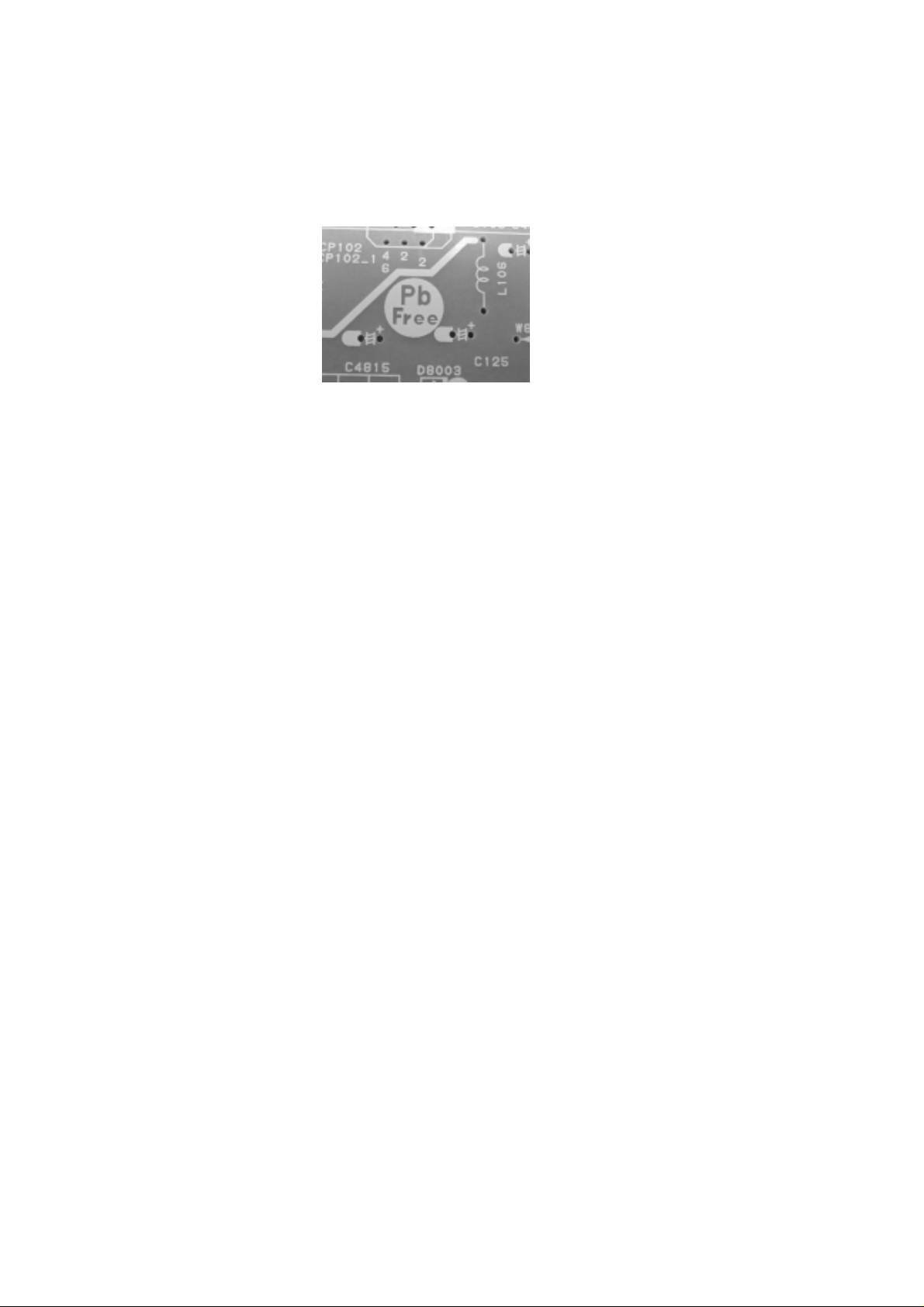
Distinction of PbF PCB:
PCBs (manufactured) using lead free solder will have a PbF printing on the PCB.
(Please refer to figures.)
Caution:
Pb free solder has a higher melting point than standard solder;
•
Typically the melting point is 50°F~70°F(30°C~40°C) higher.
Please use a soldering iron with temperature control and adjust it to 650°F ± 20°F (350°C ± 10°C).
In case of using high temperature soldering iron, please be carefull not to heat too long.
Pb free solder will tend to splash when heated too high (about 1100°F/ 600°C).
•
All products with the printed circuit board with PbF printing must be serviced with lead free solder.
•
When soldering or unsoldering, completely remove all of the solder from the pins or solder area,
and be sure to heat the soldering points with the lead free solder until it melts sufficiently.
Recommendations
Recommended lead free solder composition is Sn-3.0Ag-0.5Cu.
A1-2
Page 4

CONTENTS
SERVICING NOTICES ON CHECKING..........................................................................................................
HOW TO ORDER PARTS ...............................................................................................................................
IMPORTANT....................................................................................................................................................
ABOUT LEAD FREE SOLDER (PbF).............................................................................................................
CONTENTS .....................................................................................................................................................
GENERAL SPECIFICATIONS ........................................................................................................................
DISASSEMBLY INSTRUCTIONS
1. REMOVAL OF ANODE CAP .................................................................................................................
2. REMOVAL AND INSTALLATION OF FLAT PACKAGE IC ...................................................................
SERVICE MODE LIST.....................................................................................................................................
CONFIRMATION OF HOURS USED ..............................................................................................................
WHEN REPLACING EEPROM (MEMORY) IC ...............................................................................................
ELECTRICAL ADJUSTMENTS .......................................................................................................................
BLOCK DIAGRAM ...........................................................................................................................................
PRINTED CIRCUIT BOARDS
MAIN/CRT/OPERATION/FRONT JACK/POWER SW/RELAY....................................................................
MAIN/CRT/OPERATION/FRONT JACK ......................................................................................................
SCHEMATIC DIAGRAMS
MICON/TUNER............................................................................................................................................
CHROMA/SIF/VIF/21PIN .............................................................................................................................
SOUND/AV ..................................................................................................................................................
DEFLECTION/CRT ......................................................................................................................................
TV POWER ..................................................................................................................................................
WAVEFORMS ..................................................................................................................................................
MECHANICAL EXPLODED VIEW ...................................................................................................................
MECHANICAL REPLACEMENT PARTS LIST ...............................................................................................
ELECTRICAL REPLACEMENT PARTS LIST .................................................................................................
A1-1
A1-1
A1-1
A1-2
A2-1
A3-1~A3-4
B1-1
B2-1, B2-2
C-1
C-1
C-1
D-1~D-5
E-1, E-2
F-1, F-2
F-3, F-4
G-1, G-2
G-3, G-4
G-5, G-6
G-7, G-8
G-9, G-10
H-1~H-3
I-1
J1-1
J2-1, J2-2
A2-1
Page 5
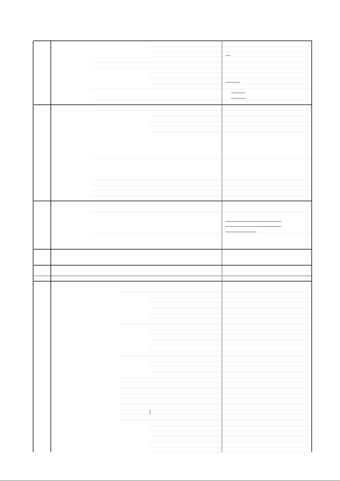
GENERAL SPECIFICATIONS
5oC
0oC
0oC
60oC
G-1 TV CRT CRT Size / Visual Size 14 inch / 335.4mmV
G-2 Tuning Broadcasting System FRANCE+CCIR System B/G L
G-3 Power Power Source AC 230V AC 50Hz
G-4 Regulation Safety CE
G-5 Temperature Operation
G-6 Operating Humidity Less than 80% RH
G-7 On Screen Menu Yes
System CRT Type Normal
Color System PAL / SECAM / MESECAM
Speaker 2 Speaker
Sound Output MAX 0.5+0.5 W
PAL60Hz Yes
System Tuner and System 1Tuner
Receive CH Destination CCIR (W/HYPER), FRENCH CATV
Intermediate PAL,SECAM(U&VH),SECAM(VL)
Frequency Picture(FP) 38.9,38.9,34.4MHz
Auto Tuning Method All Band (Not CCIR CH Plan)
Preset CH 80
StereoTV Sound (Ext Audio Input Only) Yes
Tuner Sound Muting Yes
Power Consumption at AC
Protector Power Fuse Yes
Display Menu Type Disney Character
Picture Yes
Audio No
CH Tuning Yes
Language Yes
Clock Set No
On/Off Timer Set No
Pin Code Registration No
Nicam Auto Off No
Colour System No
Sound System No
AV2 Output Source No
Control Level Yes
Deflection 90 degree
Magnetic Field BV/BH +0.45G/0.18G
Position Ext
Size 3 Inch
Impedance 8 ohm
10%(Typical) -- W
Tuning System F-Synth
Input Impedance VHF/UHF 75 ohm
CH Coverage PAL:
Sound(FS) 33.4,32.4,40.9MHz
FP-FS 5.5,6.5,6.5MHZ
DC -
Stand by (at AC) 5 W at AC 230 V 50 Hz
Per Year -- kWh/Year
Safety Circuit Yes
IC Protector(Micro Fuse) No
Radiation CE
X-Radiation PTB
Storage
Contrast Yes
Brightness Yes
Color Yes
Tint No
Sharpness Yes
Bass No
Treble No
Balance No
BBE On/Off No
Stable Sound On/Off No
Manual Yes
Auto Yes
CH Allocation Yes
Volume Yes
Brightness Yes
Contrast Yes
Color Yes
Tint (NTSC Only) No
E2 - E4, X - Z+2, S1 - S10, E5 - E12,
S11 - S41, E21 - E69
SECAM:
F2-F4, FB-FQ,F21-F69
44 W at AC 230 V 50 Hz
+
~ +4
-2
~ +
A3-1
Page 6
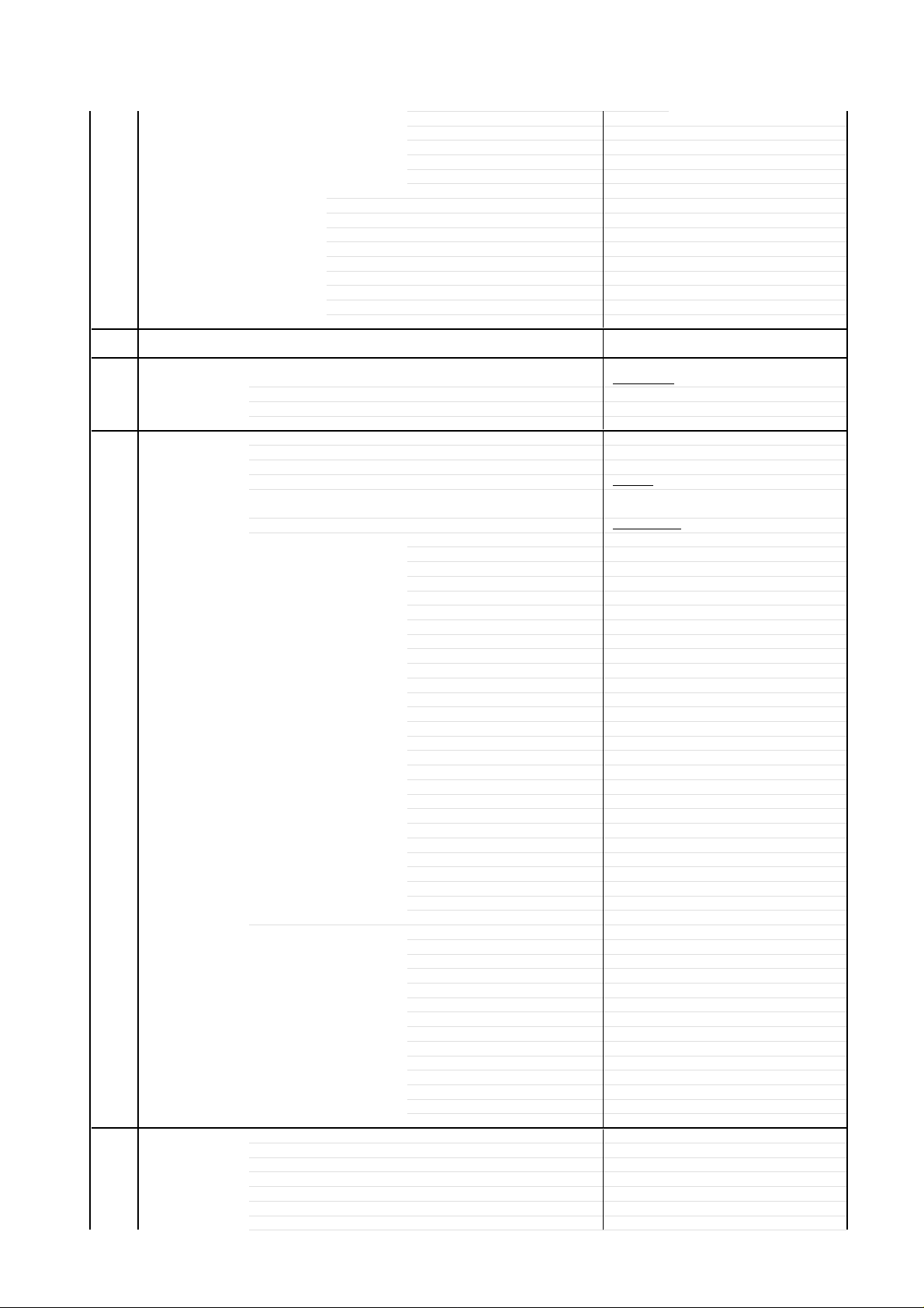
GENERAL SPECIFICATIONS
Sharpness Yes
Tuning Yes
Bass No
Treble No
Balance No
Nicam ST No
Tone 1/2 No
Pin Code No
AV Yes
Skip Yes
Channel Yes
Hotel Lock No
Sleep Timer Yes
Sound Mute Yes
G-8 OSD Language English French Spanish
G-9 Clock and Sleep Timer Max Time 120 Min
Timer Step 10 Min
On/Off Timer Program(On Timer / Off Timer) No
Wake Up Timer No
Timer Back-up (at Power Off Mode) more than -- Min Sec
G-10 Remote Unit RC-JP
Control Glow in Dark Remocon No
Format NEC
Custom Code 80-63 h
Power Source Voltage(D.C) 3V
Total Keys 24 Keys
Keys Power(Stand By) Yes
T'TEXT Keys TEXT / MIX / TV No
G-11 Features Auto Degauss Yes
Auto Shut Off Yes
Canal+ Yes
CATV Yes
Anti-theft No
Memory(Last CH) Yes
Memory(Last Volume) Yes
Back Light No
German Italian
UM size x pcs UM-4 x 2 pcs
1 Yes
2 Yes
3 Yes
4 Yes
5 Yes
6 Yes
7 Yes
8 Yes
9 Yes
0 Yes
TV/AV Yes
CH Up Yes
CH Down Yes
Volume Up / + Yes
Volume Down / - Yes
Quick View Yes
Sleep Yes
Info(CH Call) Yes
Normal No
Menu Yes
Enter No
Mute Yes
Fine Tuning + Yes
Fine Tuning - Yes
Skip Yes
Tone 1/2 No
CH Up / Page Up No
CH Down / Page Down No
Red No
Green No
Yellow / Fine Tuning - No
Cyan / Fine Tuning + No
F/T/B(Expand) / Normal No
Reveal / Skip No
Display Cancel No
Reset No
Reset / Tone 1/2 No
Hold / Status No
Sub Page / Quick View No
A3-2
Page 7
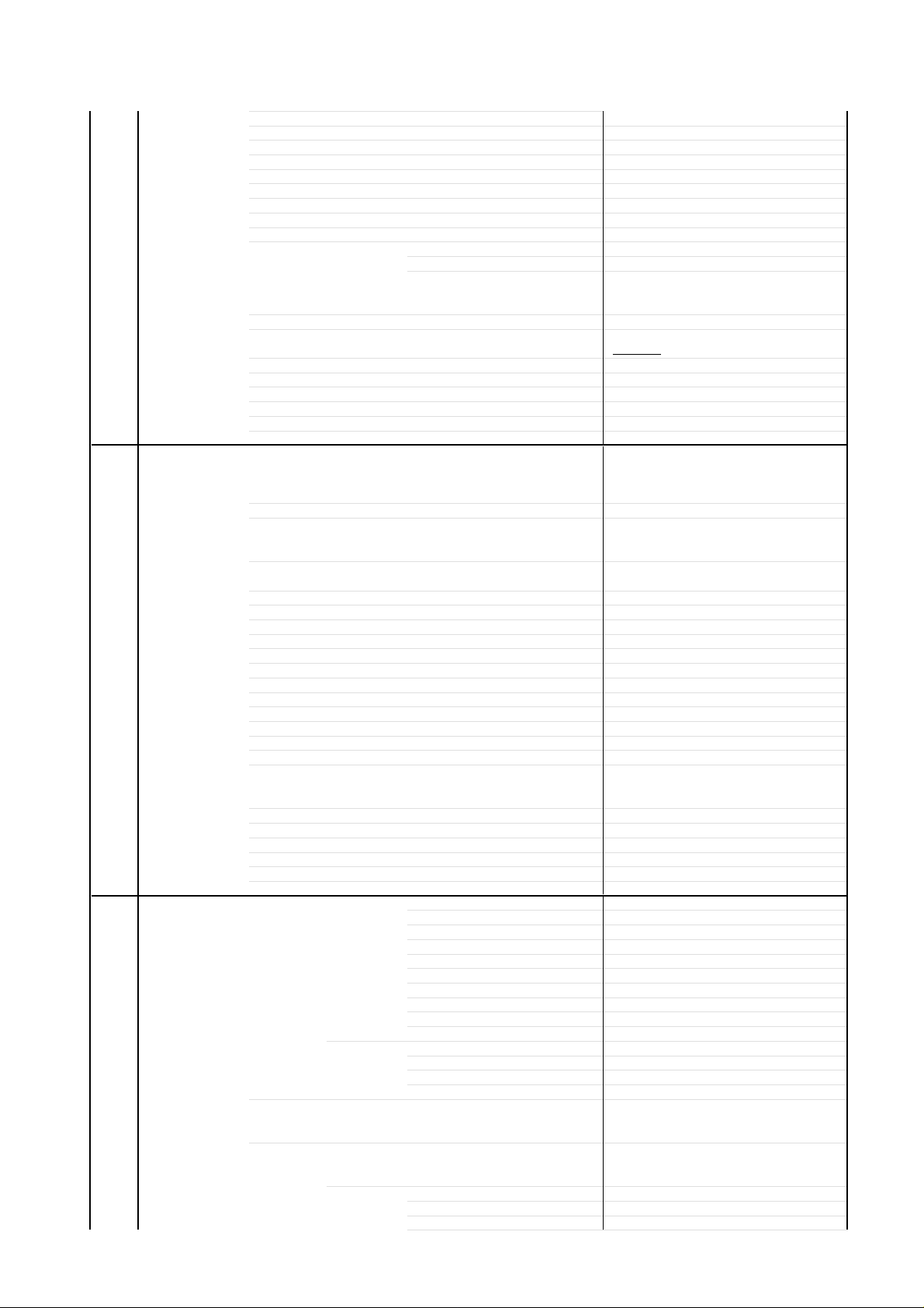
GENERAL SPECIFICATIONS
BBE No
Auto Search Yes
CH Allocation Yes
Channel Lock No
Just Clock Function No
Game Position No
CH Label No
VM Circuit No
Full OSD No
T'Text No
Premiere No
Comb Filter No
Auto CH Memory Yes
Auto Set Up No
Stable Sound No
FBT Leak Test Protect No
Hotel Lock No
Power On Memory Yes
G-12 Accessories Owner's Manual Language Einglish/Germany/French/Spanish
Remote Control Unit Yes
Rod Antenna
Loop Antenna
U/V Mixer
DC Car Cord (Center+)
Guarantee Card Yes
Warning Sheet
Circuit Diagram
Antenna Change Plug
Service Facility List
Important Safeguard
Dew/AHC Caution Sheet
AC Plug Adapter
Short Instbook (Spa/Por/IT/Dutch/Fin/Swe/Dan/Nor)
Quick Set-up Sheet
Battery Yes
AC Cord
AV Cord (2Pin-1Pin)
Registration Card
Safety Strap
Printed Matter for Disney
300 ohm to 75 ohm Antenna Adapter
G-13 Interface Switch Front Power No
Rear AC/DC No
Indicator Power No
Terminals Front Video Input RCA x1
Rear Video Input(Rear1)
Text type Text Language -
Lines
Portuguese/Italian/Dutch/Finnish
w/Guarantee Card
Poles Terminal -
Terminal -
UM size x pcs UM-4 x 2 pcs
OEM Brand
System Select No
Main Power SW Yes
Sub Power No
Channel Up Yes
Channel Down Yes
Volume Up Yes
Volume Down Yes
Menu Yes
TV/AV Yes
TV/CATV Selector No
Degauss No
Main Power SW No
Stand-by Yes
On Timer No
Audio Input RCA x2
Other Terminal
Video Input(Rear2)
Audio Input(Rear1)
Swedish/Danish/Norwegian
No
No
No
No
No
No
No
No
No
No
No
No
No
No
No
No
No
No
No
No
No
Head Phone
No
No
No
A3-3
Page 8
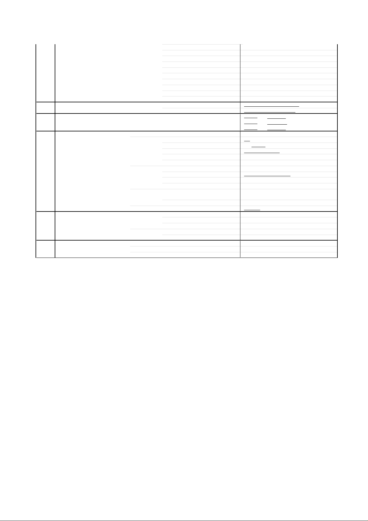
GENERAL SPECIFICATIONS
s
Audio Input(Rear2)
Video Output
Audio Output
Euro Scart(21Pin) Yes ( x1 )
Component Input
Diversity No
Ext Speaker No
DC Jack 12V(Center +) No
VHF/UHF Antenna Input
AC Outlet No
G-14 Set Size Approx. W x D x H (mm) 401.5 x 371 x 465.5
w/o Speaker,Legs Approx. W x D x H (mm)
G-15 Weight Net (Approx.) 11.0kg
Net w/o Speaker,Legs Approx. 9.5 kg
Gross (Approx.) 13.5kg
G-16 Carton Master Carton
Content ---Material --
Dimensions W x D x H(mm) -- x -- x --
Description of Origin
Gift Box Yes
Material Double/Full Color
Dimensions W x D x H(mm) 493 x 423 x 465
Design As per Buyer's
Description of Origin
Drop Test
Height (cm) 62
Container Stuffing
G-17 Material Cabinet Cabinet Front PS 94HB
Cabinet Rear PS 94HB
Cover Yes
PCB Non-Halogen Demand
Eyelet Demand
G-18 Environment Environmental
Pb-free Phase3 (Phase3A)
WEEE Yes
Din Type
401.5 x 371 x 350
Natural Dropping At 1 Corner / 3 Edges / 6
640
Green procurement of ORION
No
No
No
No
( 24.3lbs)
( 20.9lbs )
( 29.8lbs)
No
Sets
/--
No
No
Surfaces
Sets/40' container
No
No
A3-4
Page 9
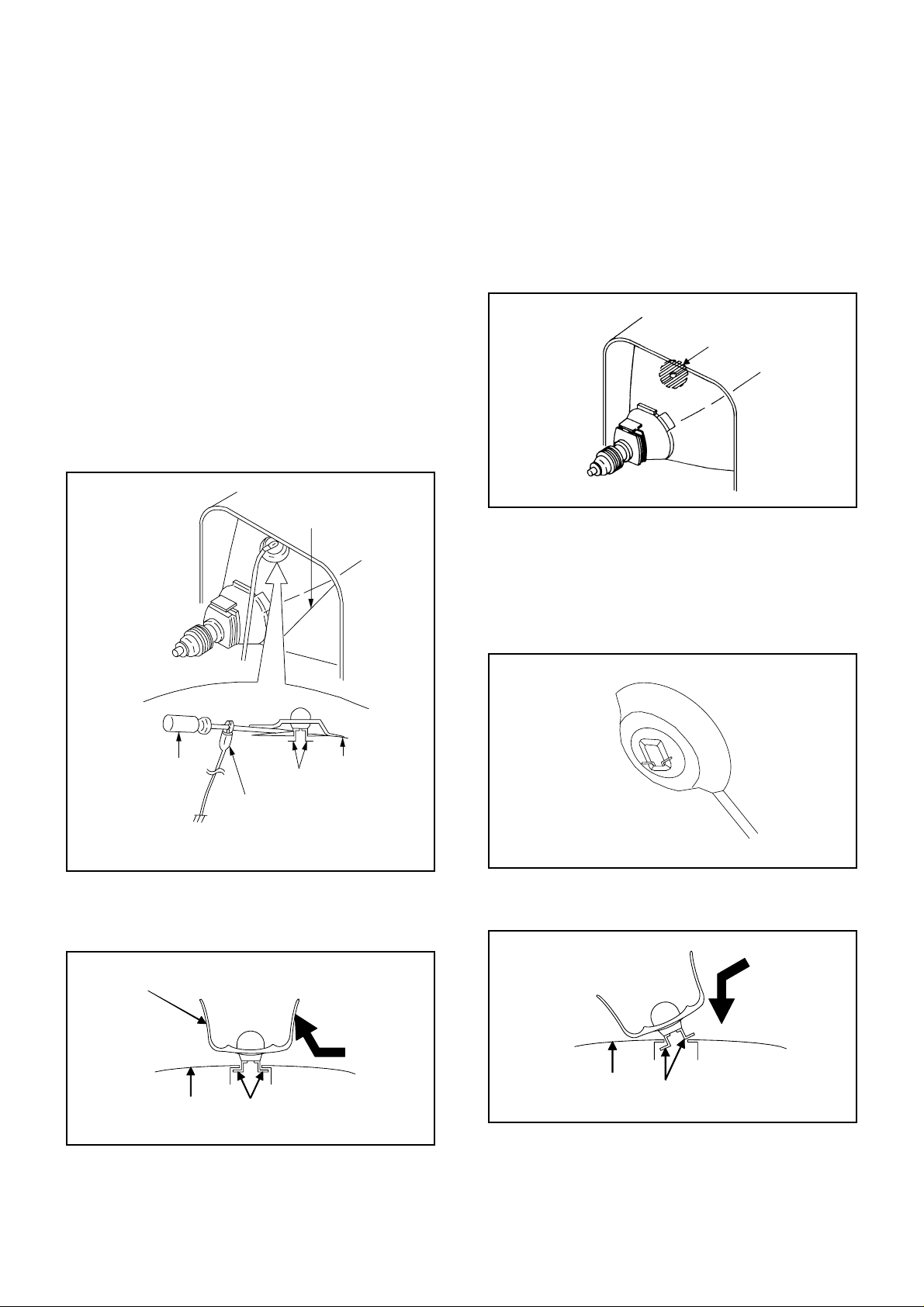
DISASSEMBLY INSTRUCTIONS
1. REMOVAL OF ANODE CAP
Read the following NOTED items before starting work.
After turning the power off there might still be a potential
*
voltage that is very dangerous. When removing the
Anode Cap, make sure to discharge the Anode Cap's
potential voltage.
Do not use pliers to loosen or tighten the Anode Cap
*
terminal, this may cause the spring to be damaged.
REMOVAL
1. Follow the steps as follows to discharge the Anode Cap.
(Refer to Fig. 1-1.)
Connect one end of an Alligator Clip to the metal part of
a flat-blade screwdriver and the other end to ground.
While holding the plastic part of the insulated screwdriver,
touch the support of the Anode with the tip of the
screwdriver.
A cracking noise will be heard as the voltage is discharged.
GND on the CRT
3. After one side is removed, pull in the opposite direction to
remove the other.
NOTE
Take care not to damage the Rubber Cap.
INSTALLATION
1. Clean the spot where the cap was located with a small
amount of alcohol. (Refer to Fig. 1-3.)
Location of Anode Cap
Fig. 1-3
NOTE
Confirm that there is no dirt, dust, etc. at the spot where
the cap was located.
2.3.Arrange the wire of the Anode Cap and make sure the
wire is not twisted.
Turn over the Rubber Cap. (Refer to Fig. 1-4.)
Screwdriver
Alligator Clip
GND on the CRT
Flip up the sides of the Rubber Cap in the direction of the
2.
arrow and remove one side of the support.
(Refer to Fig. 1-2.)
Rubber Cap
CRT
Support
Support
CRT
Fig. 1-1
Fig. 1-2
Fig. 1-4
4. Insert one end of the Anode Support into the anode button,
then the other as shown in Fig. 1-5.
CRT
Support
Fig. 1-5
5.6.Confirm that the Support is securely connected.
Put on the Rubber Cap without moving any parts.
B1-1
Page 10
DISASSEMBLY INSTRUCTIONS
2.
REMOVAL AND INSTALLATION OF
FLAT PACKAGE IC
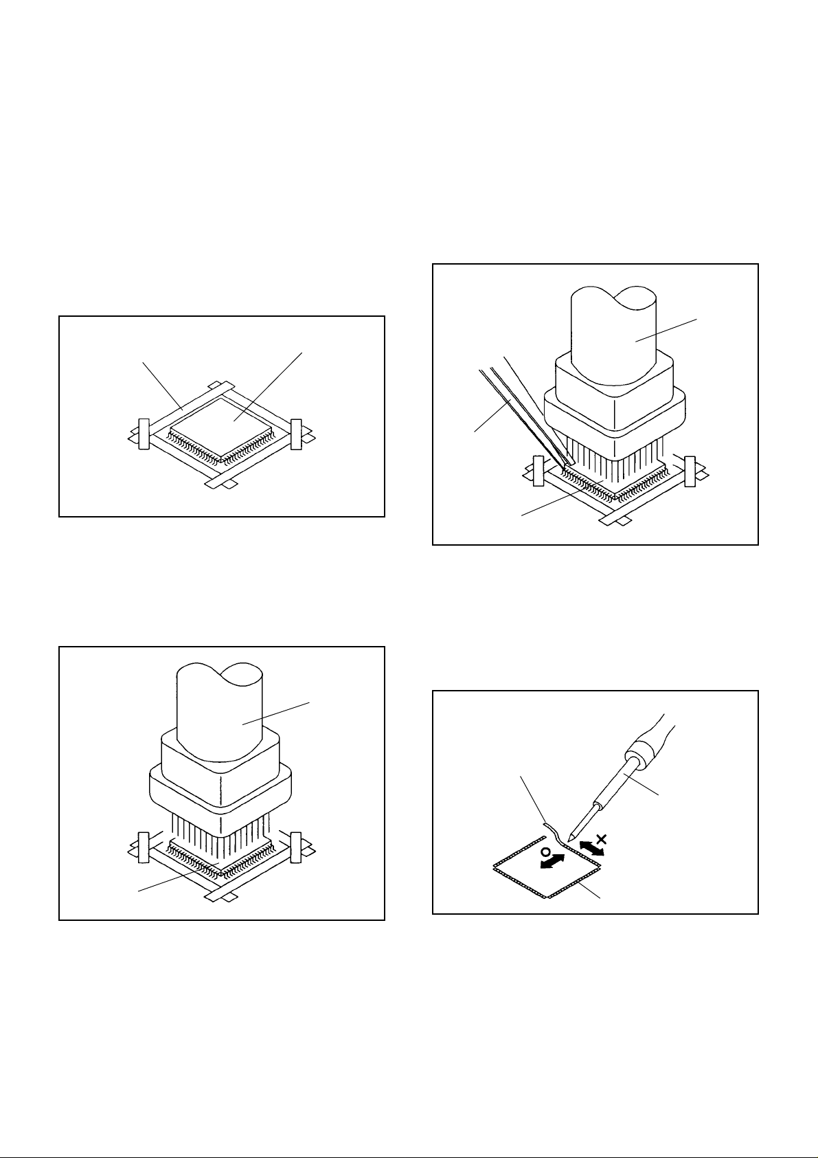
REMOVAL
Put Masking Tape (cotton tape) around the Flat Package
1.
IC to protect other parts from any damage.
(Refer to Fig. 2-1.)
NOTE
Masking is carried out on all the parts located within
10 mm distance from IC leads.
When IC starts moving back and forth easily after
3.
desoldering completely, pickup the corner of the IC using
a tweezers and remove the IC by moving with the IC
desoldering machine. (Refer to Fig. 2-3.)
NOTE
Some ICs on the PCB are affixed with glue, so be
careful not to break or damage the foil of each IC
leads or solder lands under the IC when removing it.
Blower type IC
desoldering
machine
Masking Tape
(Cotton Tape)
Heat the IC leads using a blower type IC desoldering
2.
IC
machine. (Refer to Fig. 2-2.)
NOTE
Do not rotate or move the IC back forth until IC can
move back and forth easily after desoldering the
leads completely.
Blower type IC
desoldering machine
Fig. 2-1
Tweezers
IC
Peel off the Masking Tape.4.
Absorb the solder left on the pattern using the Braided
5.
Shield Wire. (Refer to Fig. 2-4.)
NOTE
Do not move the Braided Shield Wire in the vertical
direction towards the IC pattern.
Fig. 2-3
Braided Shield Wire
Soldering Iron
IC
Fig. 2-2
IC pattern
Fig. 2-4
B2-1
Page 11
DISASSEMBLY INSTRUCTIONS
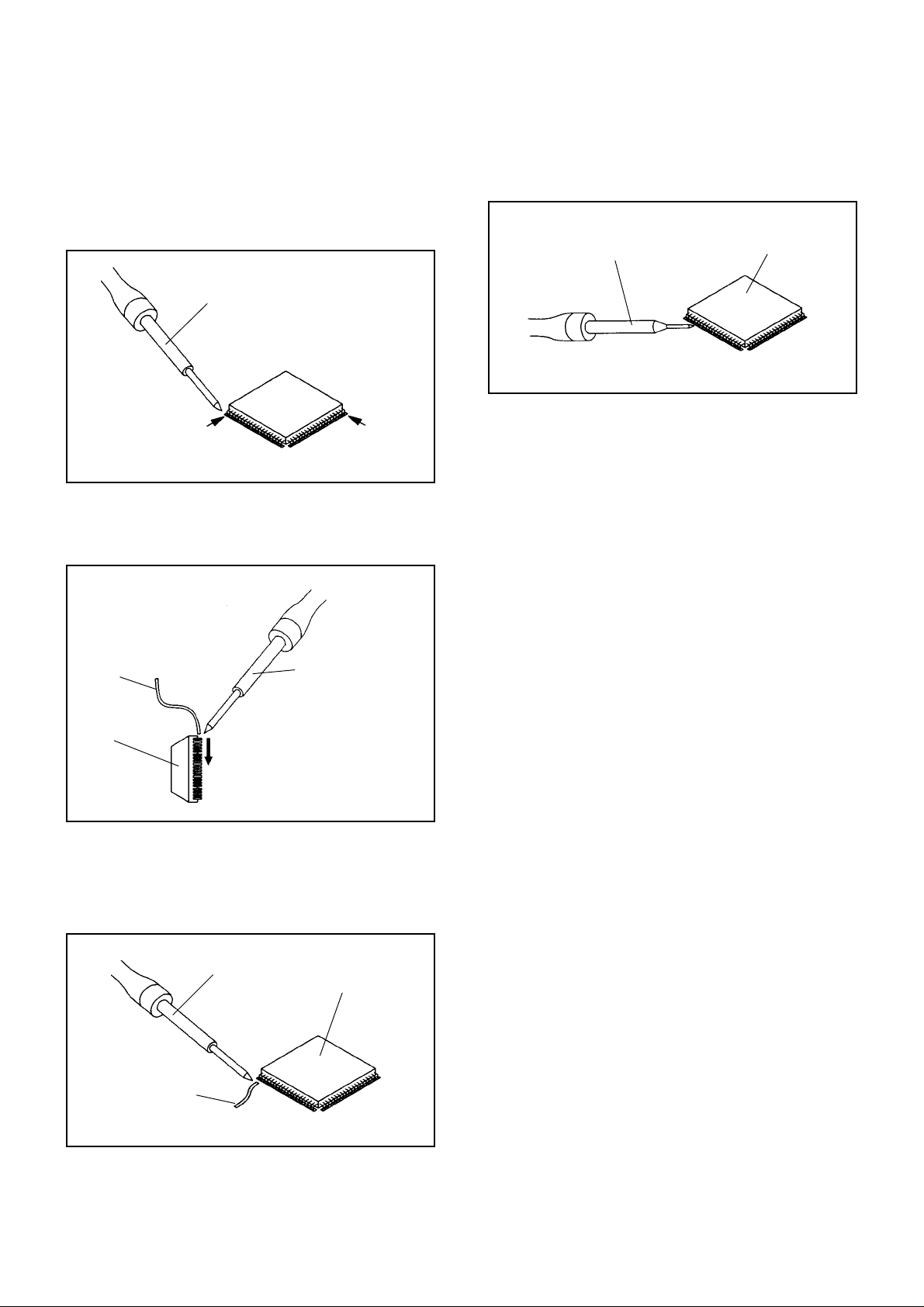
INSTALLATION
Take care of the polarity of new IC and then install the
1.
new IC fitting on the printed circuit pattern. Then solder
each lead on the diagonal positions of IC temporarily.
(Refer to Fig. 2-5.)
Soldering Iron
Solder temporarily
Supply the solder from the upper position of IC leads
2.
Solder temporarily
sliding to the lower position of the IC leads.
(Refer to Fig. 2-6.)
Fig. 2-5
When bridge-soldering between terminals and/or the
4.
soldering amount are not enough, resolder using a Thintip Soldering Iron. (Refer to Fig. 2-8.)
Thin-tip Soldering Iron
IC
Fig. 2-8
Finally, confirm the soldering status on four sides of the
5.
IC using a magnifying glass.
Confirm that no abnormality is found on the soldering
position and installation position of the parts around the
IC. If some abnormality is found, correct by resoldering.
NOTE
When the IC leads are bent during soldering and/or
repairing, do not repair the bending of leads. If the
bending of leads are repaired, the pattern may be
damaged. So, be always sure to replace the IC in this
case.
Soldering IronSolder
IC
Absorb the solder left on the lead using the Braided
3.
Supply soldering
from upper position
to lower position
Shield Wire. (Refer to Fig. 2-7.)
NOTE
Do not absorb the solder to excess.
Soldering Iron
IC
Braided Shield Wire
Fig. 2-6
Fig. 2-7
B2-2
Page 12
SERVICE MODE LIST
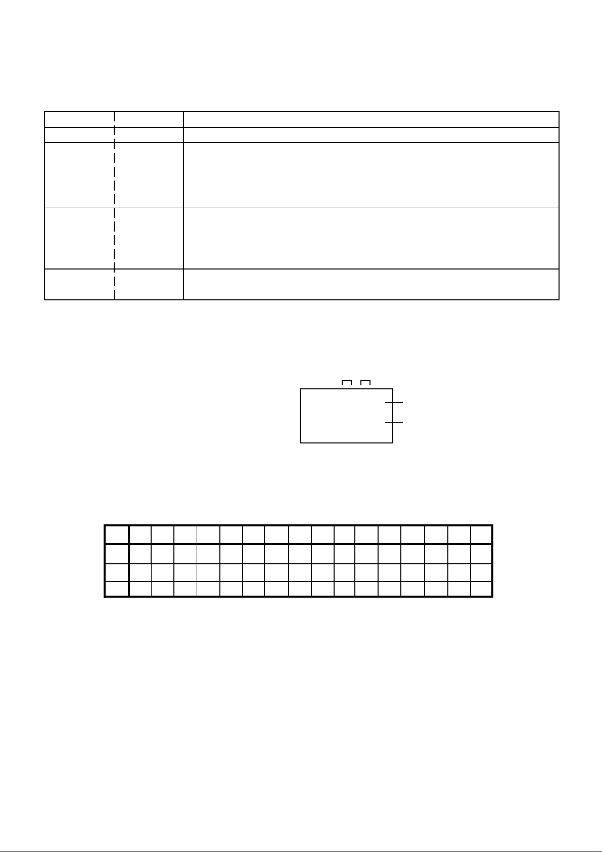
This unit is provided with the following SERVICE MODES so you can repair, examine and adjust easily.
To enter the Service Mode, press both set key and remote control key for more than 1 second.
Set Key
VOL. (-) MIN
VOL. (-) MIN 1
VOL. (-) MIN
VOL. (-) MIN
Remocon Key Operations
0
6
9
Releasing of V-CHIP PASSWORD and LOCK PASSWORD.
Initialization of factory data.
NOTE: Do not use this for normal servicing.
If you set factory initialization, the memories are reset such as the clock
setting, the channel setting, the POWER ON total hours, and PLAY/REC
total hours.
POWER ON total hours is displayed on the screen.
Refer to the "CONFIRMATION OF HOURS USED".
Can be checked of the INITIAL DATA of MEMORY IC.
Refer to the "WHEN REPLACING EEPROM (MEMORY) IC".
Display of the Adjustment MENU on the screen.
Refer to the "ELECTRICAL ADJUSTMENT" (On-Screen Display Adjustment).
CONFIRMATION OF HOURS USED
POWER ON total hours can be checked on the screen. Total hours are displayed in 16 system of notation.
NOTE: If you set factory initialization, the total hours is reset to "0".
Set the VOLUME to minimum.
1.
Press both VOL. DOWN button on the set and Channel
2.
button (6) on the remote control for more than 1 second.
After the confirmation of using hours, turn off the power.
3.
ADDRESS DATA
INIT 00 04
CRT ON 0010
FIG. 1
Initial setting content of MEMORY IC.
POWER ON total hours.
= (16 x 16 x 16 x thousands digit value)
+ (16 x 16 x hundreds digit value)
+ (16 x tens digit value)
+ (ones digit value)
WHEN REPLACING EEPROM (MEMORY) IC
If a service repair is undertaken where it has been required to change the MEMORY IC, the following steps should be taken to
ensure correct data settings while making reference to TABLE 1.
INI
+0 +1 +2 +3 +4 +5 +6 +7 +8 +9 +A +B +C +D +E +F
00 00 00 00 00 C2 AA
04 74 60 90 82 02 00 00 3F 00
8A C0 40 06 00 70 C4 00 00 00 80 00 4A 00 00
0210
00 00 00 00 00 00 00 00 00 0020 00 00 00 00 00 00
Table 1
1.
Enter DATA SET mode by setting VOLUME to minimum.
2.
While holding down VOLUME button on front cabinet, press key 6 on remote control for more than 1 second.
ADDRESS and DATA should appear as FIG 1.
3.
ADDRESS is now selected and should "blink". Using the VOL. +/- button on the remote, step through the ADDRESS until
required ADDRESS to be changed is reached.
4.
Press ENTER to select DATA. When DATA is selected, it will "blink".
5.
Again, step through the DATA using VOL. +/- button until required DATA value has been selected.
6.
Pressing ENTER will take you back to ADDRESS for further selection if necessary.
7.
Repeat steps 3 to 6 until all data has been checked.
8.
When satisfied correct DATA has been entered, turn POWER off (return to STANDBY MODE) to finish DATA input.
After the data input, set to the initializing of shipping.
9.
Turn POWER on.
10.
While holding down VOLUME button on front cabinet, press key 1 on remote control for more than 1 second.
11.
After the finishing of the initializing of shipping, the unit will turn off automatically.
C-1
Page 13
ELECTRICAL ADJUSTMENTS
BEFORE MAKING ELECTRICAL
1.
ADJUSTMENTS
Read and perform these adjustments when repairing the
circuits or replacing electrical parts or PCB assemblies.
CAUTION
Use an isolation transformer when performing any
•
service on this chassis.
Before removing the anode cap, discharge electricity
•
because it contains high voltage.
When removing a PCB or related component, after
•
unfastening or changing a wire, be sure to put the wire
back in its original position.
When you exchange IC and Transistor with a heat sink,
•
apply silicon grease (YG6260M) on the contact
section of the heat sink. Before applying new silicon
grease, remove all the old silicon grease. (Old grease
may cause damages to the IC and Transistor.)
Prepare the following measurement tools for electrical
adjustments.
1. Oscilloscope
2. Digital Voltmeter
3. Pattern Generator
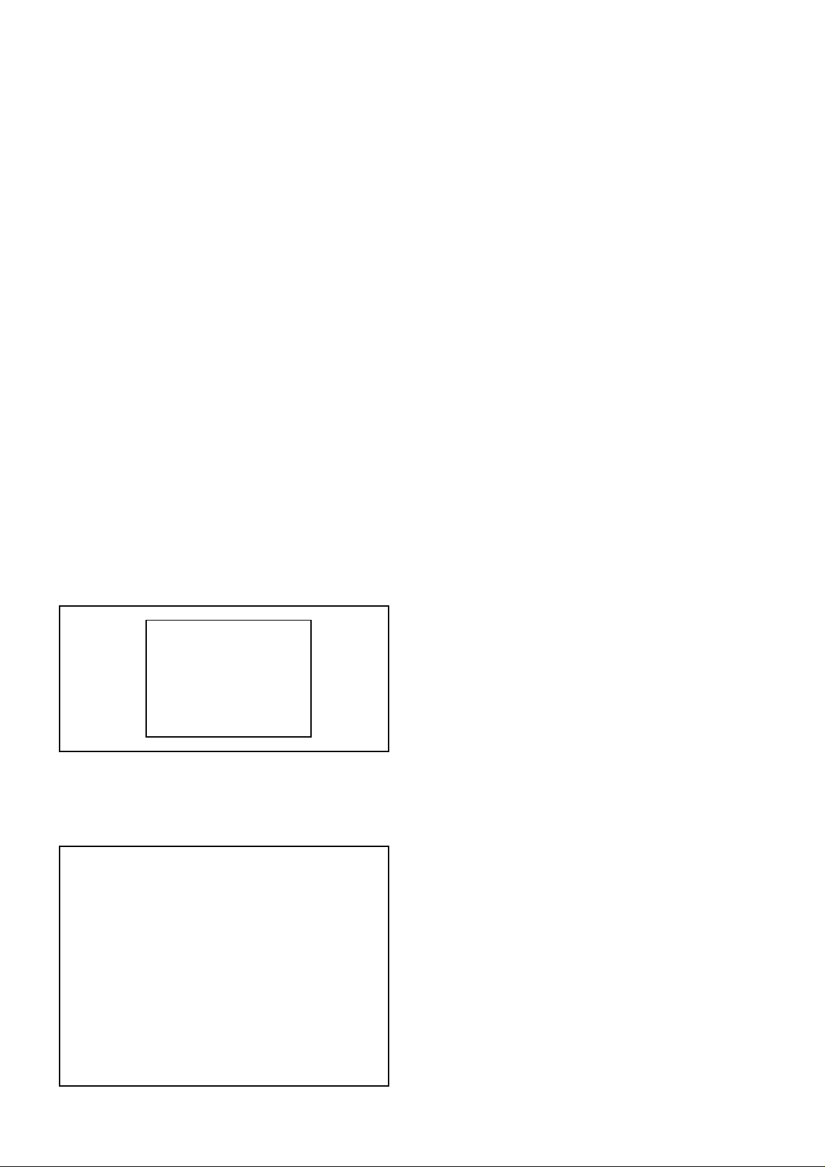
On-Screen Display Adjustment
1.
In the condition of NO indication on the screen.
Press the VOL. DOWN button on the set and the
Channel button (9) on the remote control for more than
2 seconds to appear the adjustment mode on the
screen as shown in Fig. 1-1.
TV
01 RF AGC 34
Fig. 1-1
Use the Channel UP/DOWN button or Channel button
2.
(0-9) on the remote control to select the options shown
in Fig. 1-2.
Press the MENU button on the remote control to end
3.
the adjustments.
2. BASIC ADJUSTMENTS
2-1: AGC VOLTAGE
1.
Place the set in Aging Test for more than 15 minutes.
2.
Receive the UHF (63 ± 1dB).
3.
Connect the digital voltmeter between the TP001 and
the GND.
4.
Activate the adjustment mode display of Fig. 1-1 and
press the channel button (01) on the remote control to
select "RF AGC".
5.
Press the VOL. UP/DOWN button on the remote control
until the digital voltmeter is 2.4 ± 0.05V.
2-2: CUT OFF
Place the set in Aging Test for more than 15 minutes.
1.
Using the remote control, set the brightness and contrast
2.
to normal position.
Activate the adjustment mode display of Fig. 1-1 and
3.
press the channel button (00) on the remote control to
select "CUT OFF".
Adjust the Screen Volume until a dim raster is obtained.
4.
2-3: WHITE BALANCE
NOTE: Adjust after performing CUT OFF adjustment.
1.
Place the set in Aging Test for more than 10 minutes.
2.
Receive the white 100% signal from the Pattern
Generator.
3.
Using the remote control, set the brightness and
contrast to normal position.
4.
Activate the adjustment mode display of Fig. 1-1 and
press the channel button (29) on the remote control to
select "M R CUT OFF".
5.
Using the VOL. UP/DOWN button on the remote control,
adjust the M R CUT OFF.
6.
Press the CH. UP/DOWN button on the remote control
to select the "R DRIVE", "G DRIVE", or "M G CUT OFF".
7.
Using the VOL. UP/DOWN button on the remote control,
adjust the R DRIVE, G DRIVE, M G CUT OFF or M R
CUT OFF.
8.
Perform the above adjustments 6 and 7 until the white
color is achieved.
2-4: FOCUS
1.
Receive the monoscope pattern.
2.
Turn the Focus Volume fully counterclockwise once.
3.
Adjust the Focus Volume until picture is distinct.
FUNCTION
NO.
CUT OFF
00
RF AGC
01
AGC GAIN
02
R DRIVE
03
R CUT OFF
04
G DRIVE
05
G CUT OFF
06
B DRIVE
07
H POSI
08
V POSI
10
V SIZE
12
VCO COASE
14
VCO FINE
15
VCO COASE L1
16
VCO FINE L1
17
BRIGHT CENT
18
BRIGHT MAX
19
BRIGHT MIN
20
NO.
21
22
23
24
25
26
28
29
30
31
32
33
34
35
36
FUNCTION
CONT CENT
CONT MAX
CONT MIN
COLOR CENT
COLOR MAX
COLOR MIN
SHARP
M R CUT OFF
M G CUT OFF
M B CUT OFF
CVBS OUT
APR THR
BELL
BANDPASS
H POSI OSD
Fig. 1-2
2-5: CONSTANT VOLTAGE
1.
Place the set in Aging Test for more than 15 minutes.
2.
Using the remote control, set the brightness and contrast
to normal position.
3.
Connect the digital voltmeter to W066.
4.
Set condition is AV MODE without signal.
5.
Adjust the VR501 until the digital voltmeter is 135 ± 0.5V.
D-1
Page 14
ELECTRICAL ADJUSTMENTS
2-6: HORIZONTAL POSITION
Receive the monoscope pattern.
1.
Using the remote control, set the brightness and
2.
contrast to normal position.
Activate the adjustment mode display of Fig. 1-1 and
3.
press the channel button (08) on the remote control to
select "H POSI".
Press the VOL. UP/DOWN button on the remote control
4.
until the SHIFT quantity of the OVER SCAN on right
and left becomes minimum.
2-7: VERTICAL SIZE
1.
Receive the monoscope pattern.
2.
Using the remote control, set the brightness and
contrast to normal position.
3.
Activate the adjustment mode display of Fig. 1-1 and
press the channel button (12) on the remote control to
select "V SIZE".
4.
Press the VOL. UP/DOWN button on the remote control
until the SHIFT quantity of the OVER SCAN on upside
and downside becomes 8 ± 3%.
5.
Receive a broadcast and check if the picture is normal.
2-8: BRIGHT CENT
Place the set with Aging Test for more than 15 minutes.
1.
Receive the monoscope pattern. (RF Input)
2.
Using the remote control, set the brightness and
3.
contrast to normal position.
Activate the adjustment mode display of Fig. 1-1 and
4.
press the channel button (18) on the remote control to
select "BRIGHT CENT".
Press the VOL. UP/DOWN button on the remote control
5.
until the GLAY SCALE 25% section become to be the
half black.
Receive the monoscope pattern. (Audio Video Input)
6.
Press the AV button on the remote control to set to the
7.
AV mode. Then perform the above adjustments 3~5.
2-9: CONT CENT
Place the set with Aging Test for more than 15 minutes.
1.
Activate the adjustment mode display of Fig. 1-1 and
2.
press the channel button (21) on the remote control to
select "CONT CENT".
Press the VOL. UP/DOWN button on the remote control
3.
until the cont cent step No. becomes "30".
Press the AV button on the remote control to set the AV
4.
mode. Then perform the above adjustments 1~3.
2-10: COLOR CENT
Receive the color bar pattern. (RF Input)
1.
Connect the oscilloscope to TP023.
2.
Using the remote control, set the brightness, contrast
3.
and color to normal position.
Activate the adjustment mode display of Fig. 1-1 and
4.
press the channel button (24) on the remote control to
select "COLOR CENT".
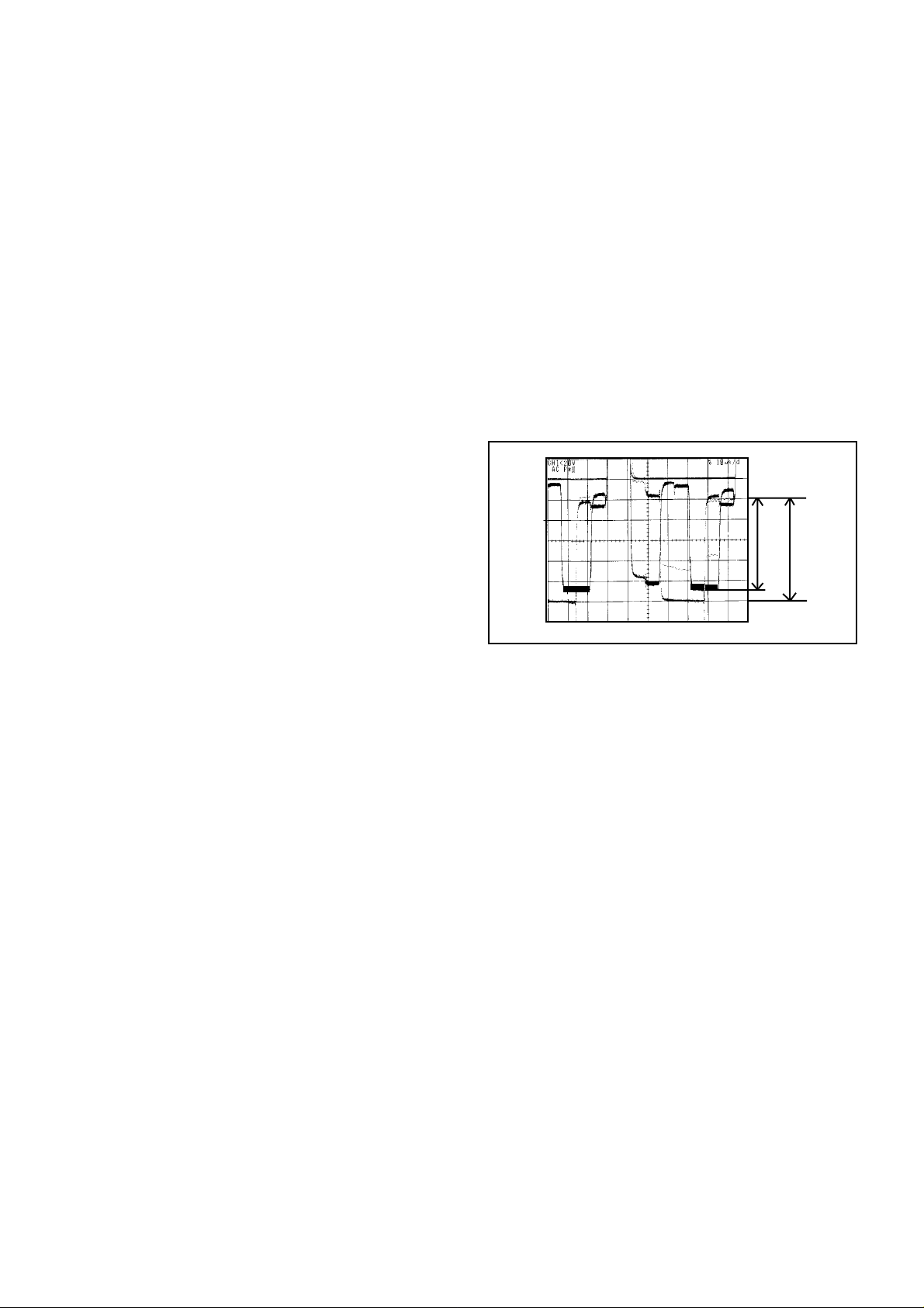
Adjust the VOLTS RANGE VARIABLE knob of the
5.
oscilloscope until the range between white 100% and
0% is set to 5 scales on the screen of the oscilloscope.
Press the VOL. UP/DOWN button on the remote
6.
control until the red color level is adjusted to 85 ± 10%
for the white level. (Refer to Fig. 2-1)
Receive the color bar pattern. (Audio Video Input)
7.
Press the AV button on the remote control to set the AV
8.
mode. Then perform the above adjustments 2~6.
100%
85%
Fig. 2-1
2-11: VCO COASE/VCO FINE
1.
Connect the oscillator (38.9MHz) to between the TP002
and the (GND) of TU001.
2.
Activate the adjustment mode display of Fig. 1-1 and
press the channel button (14) on the remote control to
select "VCO COASE".
3.
Press the VOL. UP/DOWN button on the remote control
until the "+" appear on the screen.
4.
Press the CH UP button once to set to "VCO FINE"
mode.
5.
Press the VOL. UP/DOWN button on the remote control
to select the 3 step down point from the upper limit on
the "+".
(Example: In case of the "+" point 30~41, select 37.)
2-12: VCO COASE L1/VCO FINE L1
1.
Connect the oscillator (33.95MHz) to between the TP002.
2.
Activate the adjustment mode display of Fig. 1-1 and
press the channel button (16) on the remote control to
select "VCO COASE L1".
3.
Press the VOL. UP/DOWN button on the remote control
until the "+" appear on the screen.
4.
Press the CH UP button once to set to "VCO FINE L1"
mode.
5.
Press the VOL. UP/DOWN button on the remote control
to select the 5 step down point from the upper limit on the
"+".
(Example: In case of the "+" point 30~41, select 37.)
D-2
Page 15
ELECTRICAL ADJUSTMENTS
2-13: VERTICAL POSITION
Receive the monoscope pattern.
1.
Using the remote control, set the brightness and
2.
contrast to normal position.
Activate the adjustment mode display of Fig. 1-1 and
3.
press the channel button (10) on the remote control to
select "V POSI".
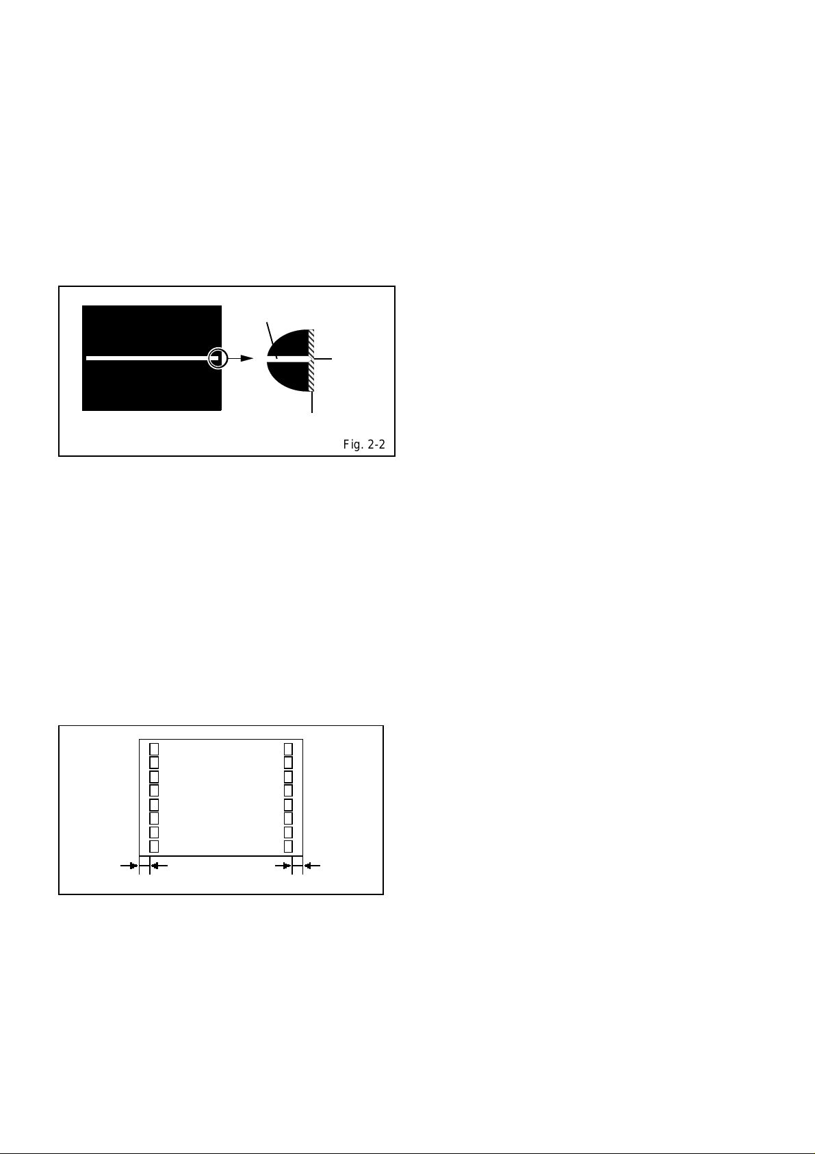
Check if the step No. V. POSI is "11".
4.
Adjust the VR401 until the horizontal line becomes fit
5.
to notch of the shadow mask. (Refer to Fig. 2-2)
horizontal line
Notch
Shadow mask
2-14: VERTICAL LINEARITY
1.
Receive the monoscope pattern.
2.
Using the remote control, set the brightness and
contrast to normal position.
3.
Adjust the VR420 until the SHIFT quantity of the OVER
SCAN on upside and downside becomes minimum.
Fig. 2-2
2-16 : Confirmation of Fixed Value (Step No.)
Please check if the fixed values of the each adjustment
items are set correctly referring below.
FUNCTION
NO.
AGC GAIN
02
R CUT OFF
04
G CUT OFF
06
B DRIVE
07
BRIGHT MAX
19
BRIGHT MIN
20
CONT MAX
22
CONT MIN
23
COLOR MAX
25
COLOR MIN
26
SHARP
28
M B CUT OFF
31
CVBS OUT
32
APR THR
33
BELL FILTER
34
BANDPASS
35
RF
00
00
00
25
35
05
55
04
48
10
12
80
12
04
00
00
AV
---
---
---
--35
05
55
04
48
10
---
---
---
---
---
---
2-15: OSD HORIZONTAL
1.
Using the remote control, set the brightness and contrast
to normal position.
2.
Activate the adjustment mode display of Fig. 1-1 and
press the channel button (36) on the remote control to
select "H POS OSD".
3.
Press the VOL. UP/DOWN button on the remote control
until the difference of A and B becomes minimum.
(Refer to Fig. 2-3)
( PAL)
TV
H POS OSD 30
A
B
Fig. 2-3
D-3
Page 16
ELECTRICAL ADJUSTMENTS
3.
PURITY AND CONVERGENCE
ADJUSTMENTS
NOTE
Turn the unit on and let it warm up for at least 30
1.
minutes before performing the following adjustments.
Place the CRT surface facing east or west to reduce the
2.
terrestrial magnetism.
Turn ON the unit and demagnetize with a Degauss Coil.
3.
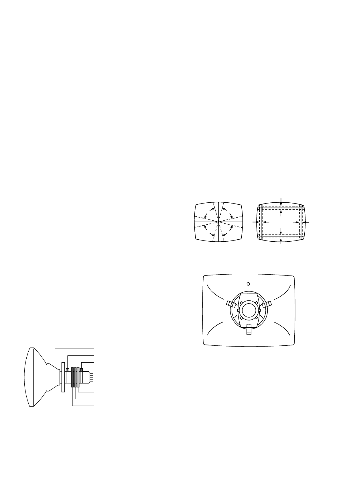
3-1: STATIC CONVERGENCE (ROUGH ADJUSTMENT)
Tighten the screw for the magnet. Refer to the adjusted
1.
CRT for the position. (Refer to Fig. 3-1)
If the deflection yoke and magnet are in one body,
untighten the screw for the body.
Receive the green raster pattern from the color bar
2.
generator.
Slide the deflection yoke until it touches the funnel
3.
side of the CRT.
Adjust center of screen to green, with red and blue on the
4.
sides, using the pair of purity magnets.
Switch the color bar generator from the green raster
5.
pattern to the crosshatch pattern.
Combine red and blue of the 3 color crosshatch pattern
6.
on the center of the screen by adjusting the pair of
4 pole magnets.
Combine red/blue (magenta) and green by adjusting the
7.
pair of 6 pole magnets.
Adjust the crosshatch pattern to change to white
8.
by repeating steps 6 and 7.
3-2: PURITY
NOTE
Adjust after performing adjustments in section 3-1.
1.
Receive the green raster pattern from color bar
generator.
2.
Adjust the pair of purity magnets to center the
color on the screen.
Adjust the pair of purity magnets so the color at the
ends are equally wide.
3.
Move the deflection yoke backward (to neck side)
slowly, and stop it at the position when the whole
screen is green.
4.
Confirm red and blue colors.
5.
Adjust the slant of the deflection yoke while watching the
screen, then tighten the fixing screw.
DEFLECTION YOKE
DEFLECTION YOKE SCREW
MAGNET SCREW
3-3: STATIC CONVERGENCE
NOTE
Adjust after performing adjustments in section 3-2.
1.
Receive the crosshatch pattern from the color bar
generator.
2.
Combine red and blue of the 3 color crosshatch pattern
on the center of the screen by adjusting the pair of
4 pole magnets.
3.
Combine red/blue (magenta) and green by adjusting the
pair of 6 pole magnets.
3-4: DYNAMIC CONVERGENCE
NOTE
Adjust after performing adjustments in section 3-3.
1.2.Adjust the differences around the screen by moving
the deflection yoke upward/downward and right/left.
(Refer to Fig. 3-2-a)
Insert three wedges between the deflection yoke and
CRT funnel to fix the deflection yoke.
(Refer to Fig. 3-2-b)
R G B
R
G
B
UPWARD/DOWNWARD SLANT RIGHT/LEFT SLANT
WEDGE
WEDGE POSITION
R
G
B
Fig. 3-2-a
WEDGE
WEDGE
Fig. 3-2-b
R G B
Fig. 3-1
PURITY MAGNETS
6 POLE MAGNETS
4 POLE MAGNETS
D-4
Page 17
ELECTRICAL ADJUSTMENTS
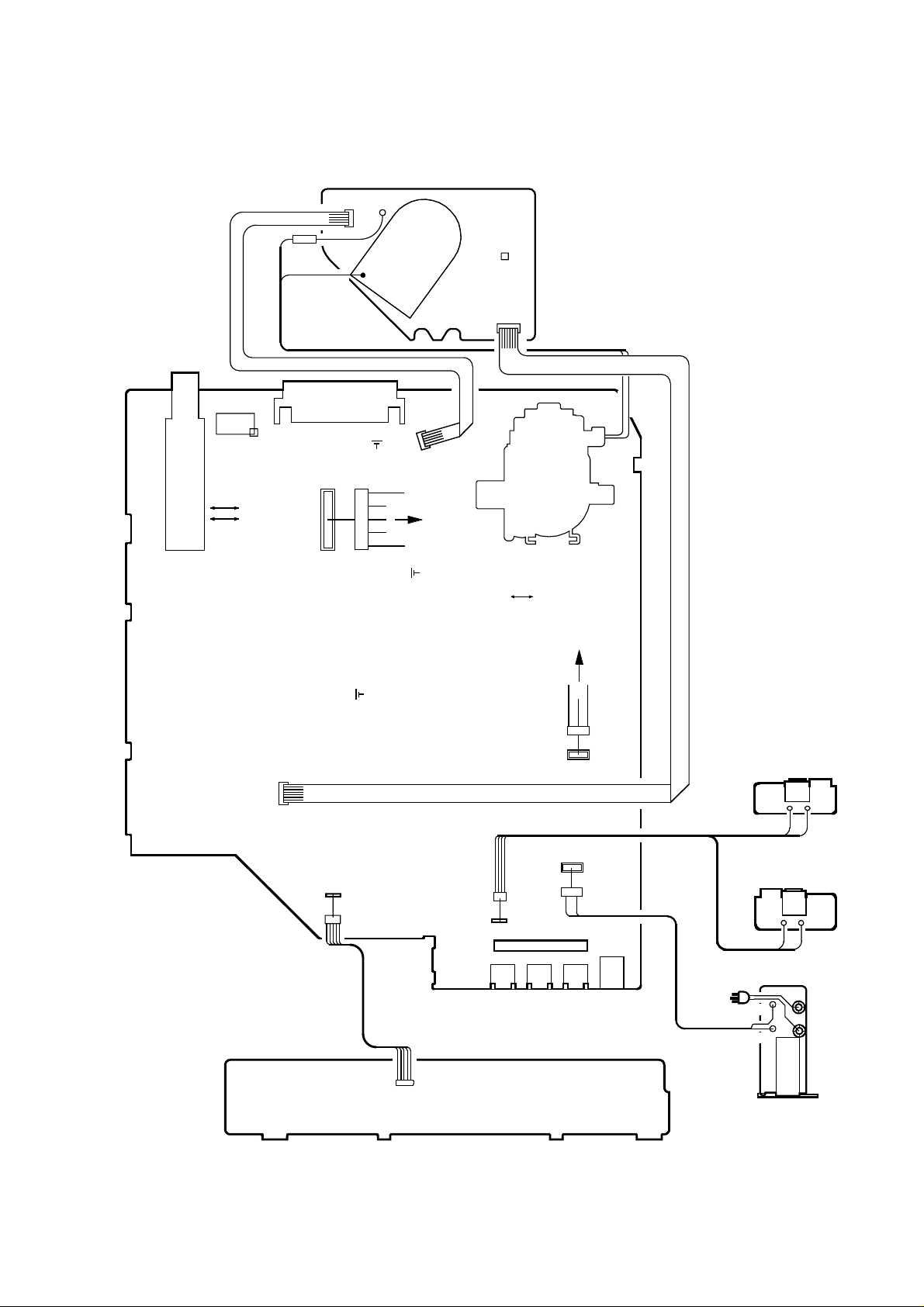
4. ELECTRICAL ADJUSTMENT PARTS LOCATION GUIDE (WIRING CONNECTION)
CRT PCB
CP806
CP803B
J801
TP023
TU001
CP102
CD803
TP001
TP002
J701
CP401
VR401
VR501
VR420
CP802B
CP803A
FB401
CRT DY
CD802
W066
DEGAUSS COIL
L503
MAIN PCB
CP802A
CP101
CD2001
CP1001
RELAY PCB
J704 J702 J703
OPERATION PCB
CP502
CP503
J1001
FRONT JACK PCB
S1152 S1153
FRONT JACK PCB
S1150 S1151
AC IN
CD501
S503A
CD503
S503B
SW501
POWER SW PCB
J1151
J1150
S501A
S501B
D-5
Page 18
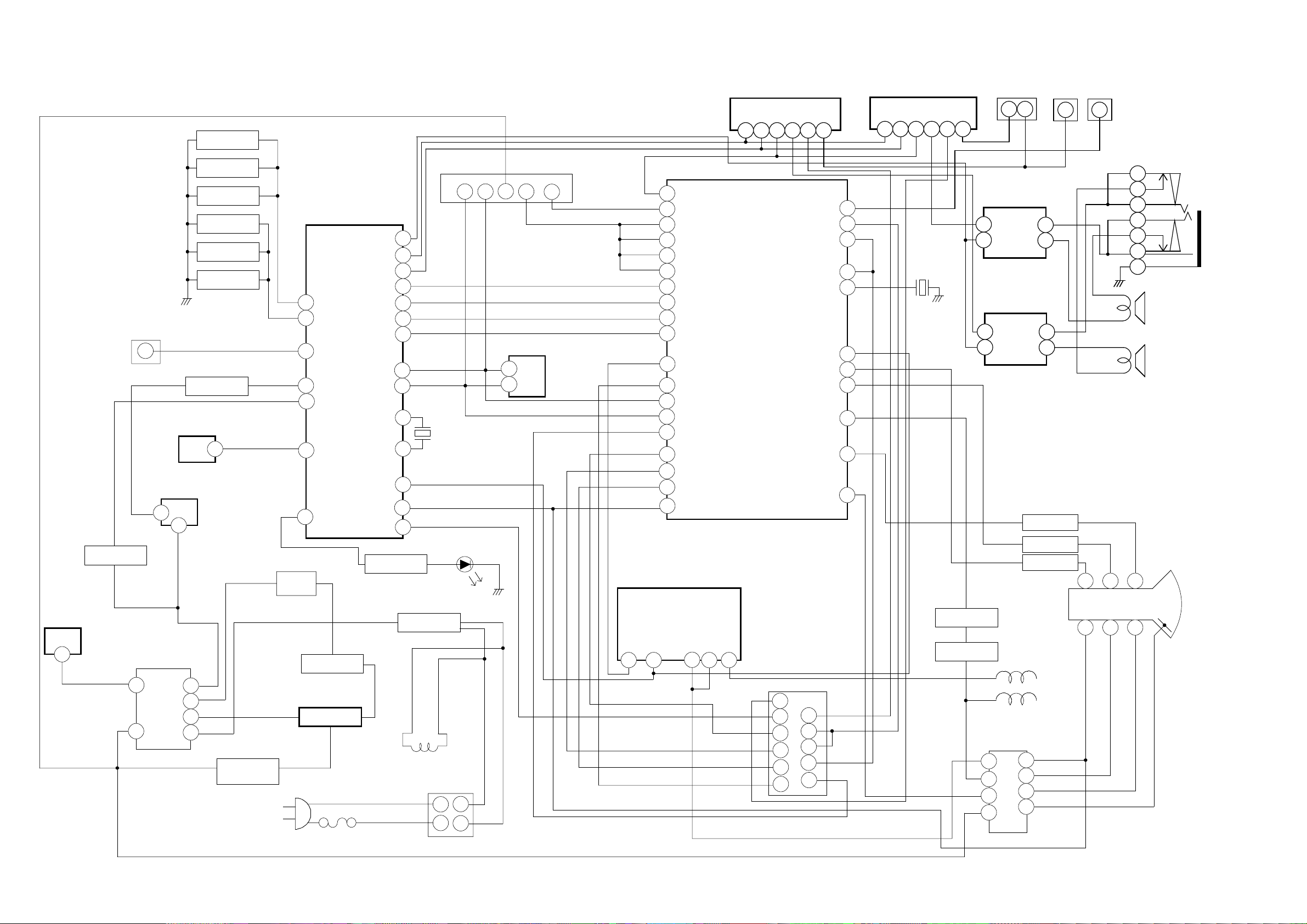
BLOCK DIAGRAM
Q506
P.FAIL
REG. 6V IC
IC502 KIA7806API
1
OS2001
1
RESET IC
IC102 PST3231NR
REG. 9V IC
IC503 KIA78R09API
4
1
T501
CH DOWN
MENU
VOL DOWN
LINE
CH UP
VOL UP
Q510, Q511
P.CON SW.
1
MICON IC
IC101 OEC7110A
8
9
15
33
4
30
11
Q501
POWER
Q502
KEY1
KEY2
REMOCON
POWER
P.FAIL
RESET
BLUE B
BLANK
V.SYNC
H.SYNC
STAND_BY_LED
SCART_IN
Q103
LED DRIVE
POWER
AV2
Xin
Xout
46VOLUME
43AV1
44
52RED R
51GREEN G
50
49
39SCL1
37SDA1
24
25
2
1
3
D501~D504
RECTIFIER
X101
8 MHz
D101
SDA
5
TU001
SCL
4
9
MEMORY IC
IC199 AT24C08AN-10SU-2.7
6
5
AGCIF
11 1
SCL
SDA
CHROMA IC
IC201 STV2248H
55 AUDIO_OUT
8
RF_AGC_OUT
SIFIN1
1
SIFIN2
2
PIFIN1
6
PIFIN2
7
OSD_R
36
OSD_G
35
OSD_B
34
OSD_BK
37
42
X1/VAMP/CHR_OUT
B_EXT/U_EXT
25
SCL
51
SDA
52
CVBSIN2
20
28
BLK_EXT
R_EXT/V_EXT
27
G_EXT/Y_EXT
26
49
LBF/SSC
IC401 TDA8174A
V-DRIVE IC
413
10
TUNER/AV1/AV2 Lch SW
IC701 NJM2534V (TE2)
4
2
INT_CVBS_OUT
2
5
1
7
Y/CVBS_IN3
FM_OUT
CVBSIN1
XTAL1
B.OUT
G.OUT
H.OUT
R.OUT
3
VERT
TUNER/AV1/AV2 Rch SW
IC702 NJM2534V (TE2)
2 4 1
22
11
18
13
40
47
48
30
49
31
48
32
46BCL/SAF
5
7
X601
4.433619MHz
Q402
H. DRIVE
Q401
H. OUTPUT
FRONT JACK
J703
3
2
3
SOUND AMP IC(Rch)
IC1001 AN7513
2
4
SOUND AMP IC(Lch)
IC1002 AN7513
2
4
Q802
Q801
GREEN OUT
Q803
J702
2
6
8
6
8
RED OUT
BLUE OUT
J704
2
397
Heater
F8
4
7
6
2
3
4
5
1
RGB
SPEAKER
SP1001
SPEAKER
SP1002
V801
CRT
HEADPHONE_JACK
J1001
E-1
15
13
17
J701
5
3
IC504 LTV-817M-VB
FEED BACK
8
Q507
FEED BACK
SWITCHING
AC IN
F501
L503
DEGAUSS COIL
L501
2
4
1
3
16
15
11
2
6
8
1
3
19
20
7
FB401
3
1
FBT
7
2
DY
10
F
S
HV
E-2
Page 19
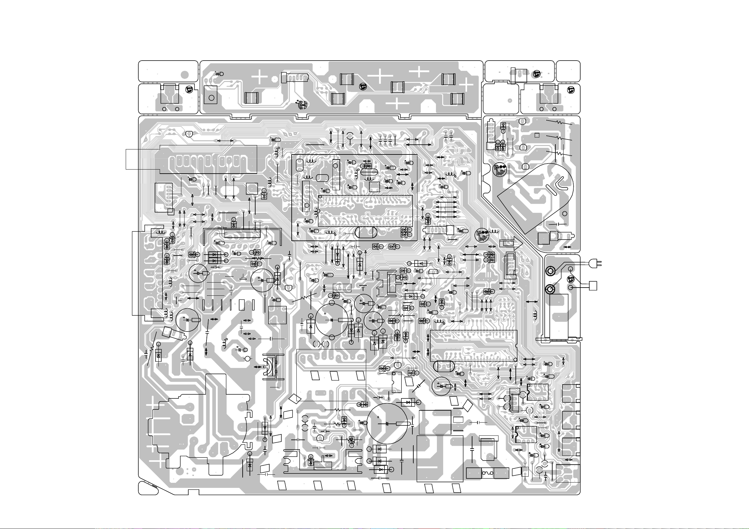
PRINTED CIRCUIT BOARDS
MAIN/CRT/OPERATION/FRONT JACK/POWER SW/RELAY (INSERTED PARTS)
SOLDER SIDE
CEE090A
S1152
L706
D706
J701
L702
R429_1
C401
J1151
D410
S1153
D703
R706
L704
W824
CP803A
CD803A
CP102
W048
D705
R708
R707
VR401
L703
C411
R119
W075
C448
Q203
C003_1
W078
W063
R710_1
D709
R703
R402
R403
W069
W076
W077
C403
D405
TU001
HS401
FB401
R005
C413
W070
C2001
R003
D403
C412
R416
R409
R410
W068
C443
W079
R412
OS2001
W064
R007
R647
C414
L401
TP001
D407
R420
C422
CP401
C423
TP002
D602
C408
VR420
C437
IC401
W067
R421
SW2007
CP001
W062
R404
D401
D402
W071
R447
R405
W072
R002
R408
C418_1
W058
R445
D414
R406
R407
Q401
D604
C435
R411
W081
C528
D001
R417
C417
C444
HS402
R427
L001
L302
C446
T401
W061
C002
W066
R305
D406
R304
R446
CD2001
CF304
C440
Q402
R520
C509
D101
L206
CF301_1R307
C611
W056
W820
W819
R001
R424
C517_1
D510
R517
L203
R514
D522
R213
C610
C533
B501
L103
C516
Q502
C507
CF204
C525
W057
D525
C521
C524
Q501
L601
R643
W060
W065
W055
B504
T501
SW2006
R621
C209
D603
IC503
R503
R502
HS501
SW2004
CF202_2
R511
W049
B1002
C629
R646
W052
W051
C506
D511
D508
L202
C217
C530
W050
R526
D505
CEE092A
W080
W047
IC201
X601
W082
R518
D517
VR501
D513
D507
C519
R523
R516
R525
D503
W046
D611
L204
L207
D610
HS502
C515
C522
D516
D528
C518_1
C503
C608
CF201
C508
D527
R529
C622
C210
W042
R510
C505
C623
C220
D609
R504
D515
C534
D502
D501
SW2003
R720
W044
C602
D608
D607
D518
IC502
R519
D529
Q507
W045
W054
IC504
W018
W043
D521
W053
D514
R530_1
R513
R512
D504
C504
C502
D523
W073
C604
D512
C514
W825
TH501
R501
W017
W028
D109
D103
D524
C527
W015
W014
W024
R524
D509
W039
W074
D606
CP802A
W023
Q511
W823
C118
W016
W013
C634
W029
W027
W025
CD802A
W022
W037
W083
L101
X101
SW2002
C712
L701
W030
W026
D105
D104
SW2005
C707
R422
W036
C115
W031
C535
L501
C710
R601
C613
R115
W035
R110
C122
W803
CME049A
W021
W020
W019
R107
R108
R125
W034
IC101
R137
W038
W041
W040
CP502
C532
C501
FH502
CEE093A
D807
CD802B
CP802B
D809
CCE042A
L707
W001
D102
D106
D107
W032
W033
W005
B1003
B1004
CP503
F501
D808
W818
W002
FH501
R809
R811
R806
W004
CP1001
C1012
W011
R814
W821
CP701
Q801
Q802
Q803
CP101
R1003
W808
W007
W006
C1005_1
W003
B1001
IC1002
C1013
B1008
TP023
J801
IC1001
B1005
W012
C1014
R1008
R807
CP801
L708
C1017
R1013
R1002
C1007
B1007
J1150
S501A
C1003
C1011
R804
B1006
C1015
S1151S1150
R803
R805
C819
CP803B
CD803B
S501B
SW501
W010
R1009_1
CEE091A
R802
CP806_1
W815
S503A
S503B
CEE102A
W008
J704
J702
J703
W009
J1001
CD501
CD503
F-1
F-2
Page 20
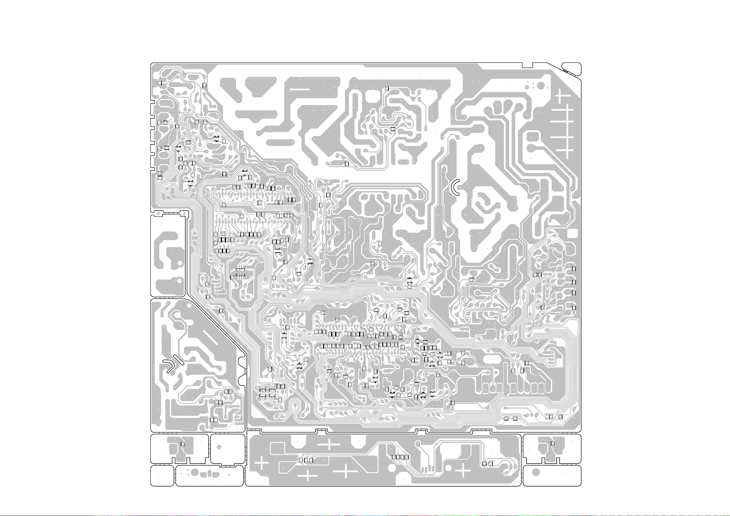
PRINTED CIRCUIT BOARDS
MAIN/CRT/OPERATION/FRONT JACK (CHIP MOUNTED PARTS)
SOLDER SIDE
C1016
R723
C715
R721
C714
R701
R712
CEE102A
R722
Q1003
R1014
R1001
R1012
R1004
Q1001
R1006
C1004
R1010
C1019
C1008
C1001_1
Q1002
R102 R123
R121
R103
R122
C136
R1011
R1005
R101
R124
R104
C139
C141
R139
R120
C101
R133
IC199
Q103
R141
R151
R153
R147
R116
R112
R132
R148
R105
C134
R150
R106
R135
R149
R130
C121
R142
IC102
R109
C120
C113
C105
R134
C104
C114
R129
R128
C102
C119
C103
R515
Q510
R532
C513
C531
C529
R507
C526
R522
Q506
R508
R419
C702
R714R715R713
C713_1
CEE091A
C1150
C1002_1
R813
C804
C805
C706
R816
R815
CME049A
CCE042A
C806
C716
IC701 IC702
Q403
C709
C711
C705
C405
Q605
R623
R2003
R2004
R2005
R630
R618
R629
C607
R628
R622
R625
C620
C619
C626
R636
C618
C603
R219
C621
R217
C630
C221
R206
C615
R608
C201
C616
R639
R204
C216
C614
C215
R644
C207
Q204
C624
R218
R208
R638
C205
R645
C625
C202
C212
C601
C213
Q201
C218
R201
R2007
R606
C612
C206
R607
R202
R2006
R602
C609
C605
C303
C204
R214
R2002
R2001
D301
R301
R215
C203
R310
R309
Q303
R306
C301C306
R312
Q302
Q304
R311
C302_1
Q301
R302
C305
R303
C304
C001
C004
C009
R2008
R2009
R709
R004
C005
C006
R702R719
C708
C1151
R221
R711
CEE090A
CEE093A
CEE092A
F-3 F-4
Page 21
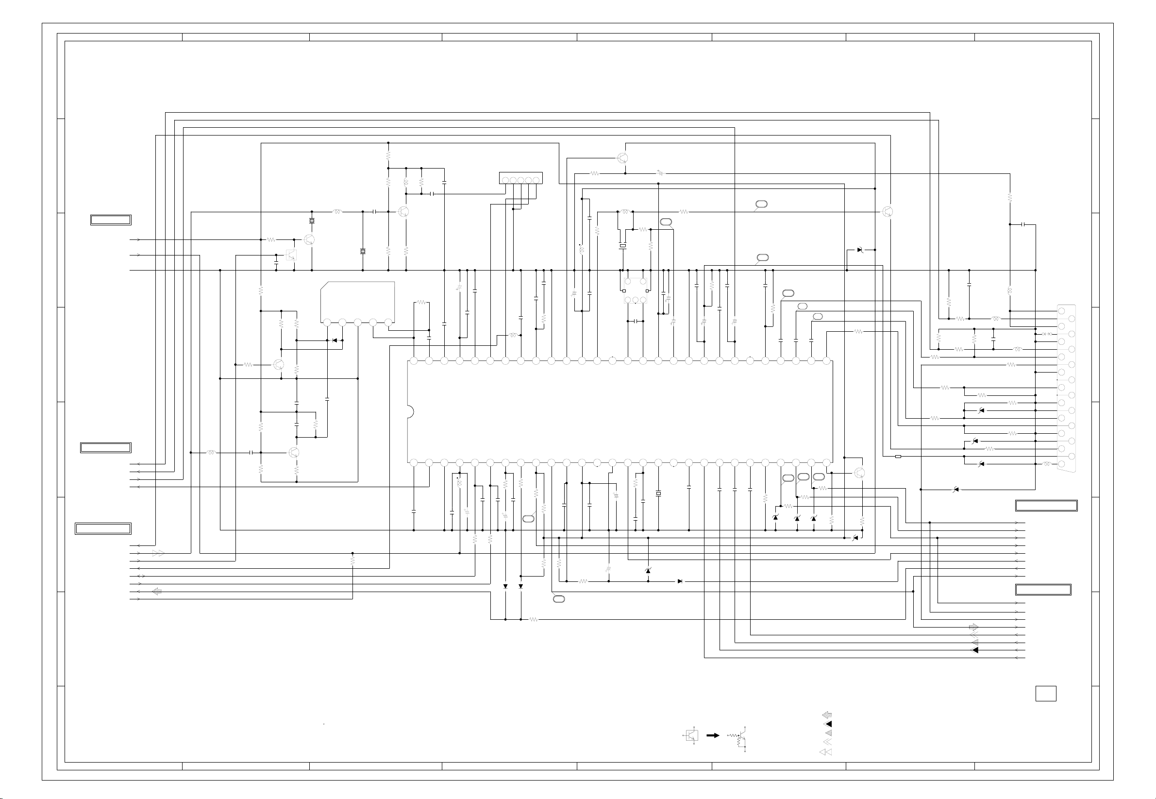
ABC DEF GH
TEST POINT
8
CP102
A2001WR2-7P
1
GND
2
SCL
3
SDA
4
I2C OFF
5
RF AGC
6
R.OUT
7
B.OUT
FROM/TO TV POWER
7
P.CON+5V
POWER
FROM/TO CHROMA/SIF/VIF/21PIN
RF_AGC
6
5
4
FROM/TO CHROMA/SIF/VIF/21PIN
B.OUT
P.CON+5V_A
R.OUT
OSD_R HD
OSD_G V_OUT
OSD_B FOR_VCR
OSD_BLK
TO SOUND/AV
VOLUME
POWER
AUDIO_MUTE
PROTECT
GND
IF
AV2
AV1
SCL
SDA
R119
3
TO DEFLECTION/CRT
PROTECT
2
1SS133
1K
R129
C105
100
4.9
4.9
0
0.1 B
100
R128
B
D104
C104
R142
0.0047
1
NOTE:THIS SCHEMATIC DIAGRAM IS THE LATEST AT THE TIME
OF PRINTING AND SUBJECT TO CHANGE WITHOUT NOTICE
ABC DEF GH
100 1/4W
RESET IC
PST3231NR
123
RESET
VCC
GND
IC102
1K1/4W
NC
NC
R110
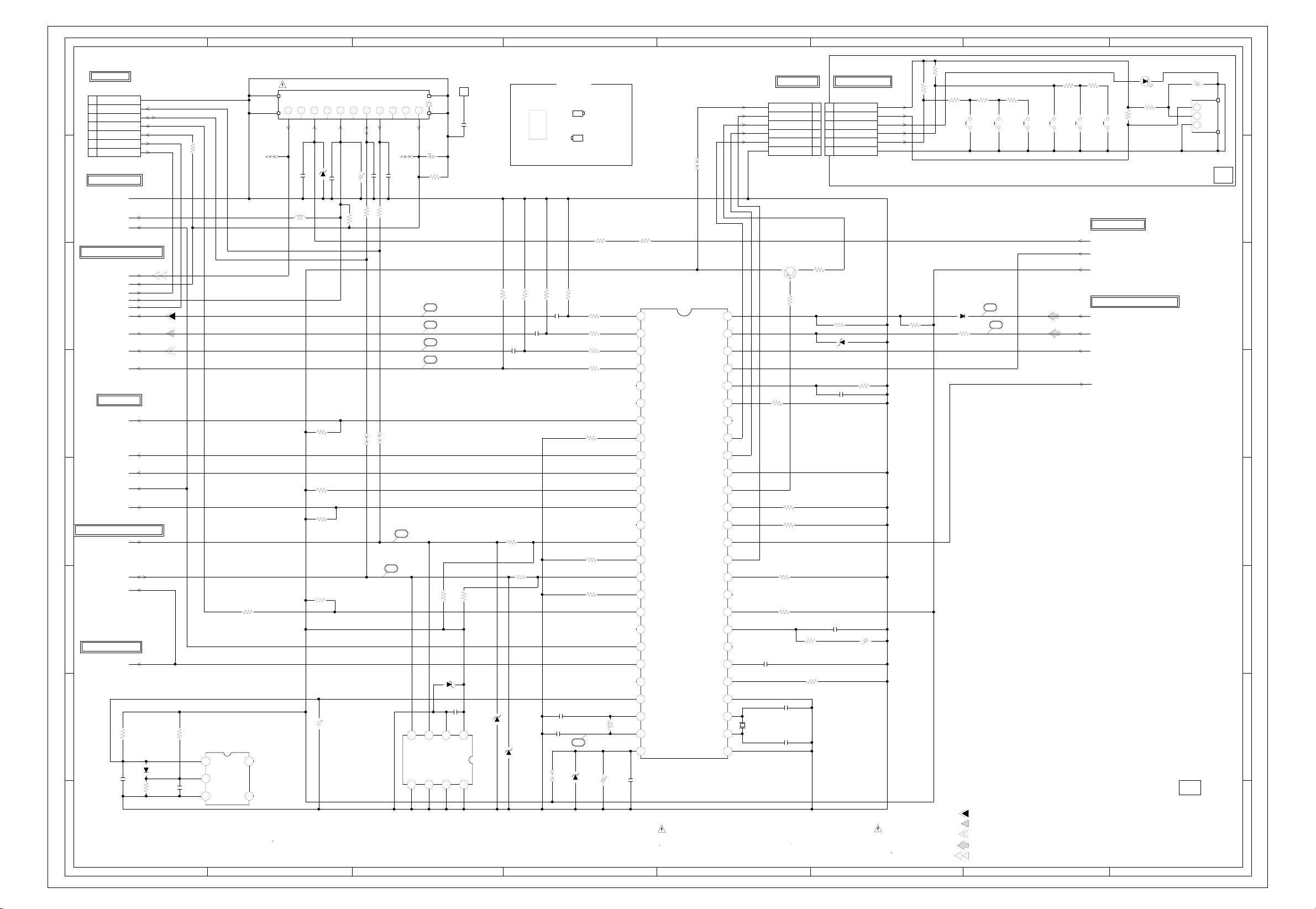
MICON/TUNER SCHEMATIC DIAGRAM
2.2K
R109
10K
R2001
R2002
2.2K
R2003
560
SW2002
VOL DOWN
D105
1SS133
R115
1K1/4W
R20041KR2005
MENU
EVQ21505R
SW2003
EVQ21505R
3
2
1.8K
SW2004
CH DOWN
VOL UP
EVQ21505R
SW2005
EVQ21505R
R2006
560
CH UP
SW2006
R2007
1K
LINE
SW2007
EVQ21505R
EVQ21505R
FROM TV POWER
+B
POWER_FAIL
AT+5V
FROM/TO CHROMA/SIF/VIF/21PIN
SECAM_VL_H
TU001 TUWRF4EG-778F2A_P3
AGC
4.8
R003
W819
SDA
5
ADRES
SCL
2
3
4
4.8
C005 56P CH
C006 56P CH
1/4W
100
W820
1
4.6
1.3NC6.2
NC
AGC
C003_1
TP001
NC
R005
100 1/4W
10
9
4.8
5678
SDA
VSS
0000
12 13
4716V KA
R004
82K
7
6
5
8
SCL
E2
BTL
BPL
IF
9
11
10
14 15
0
0
30.0
NC
IF
TP002
NC
D001 MTZJ33B
C004 0.022 B
L001
0305
10uH
R153
4.7K
R116
4.7K
R132
4.7K
R125
10K1/4W
C115
0
NC
0
4 5
NC
V.S
6
8
7
0
4.9
NC
NC
0.01 B
C001
C002 4706.3V YK
R007
15K 1/4W
0.150V KA
R105
D107
MTZJ5.6B
MODE
E1
3.3K
C101
1B
4.904.8
C009
R106
1
E0 VCC
1234
CP001
003P-2100
0.001 B
3.3K
MEMORY IC
IC199
2.2K
R104
R124
C141
0.1B
R107
1001/4W
R108
1001/4W
D106
MTZJ5.6B
D102
MTZJ5.6B
AT24C08AN-10SU-2.7
RC-JP030
TM101
1K
C139
0.1B
R103
1K
C136
0.1
C113
12P CH
C114
12P CH
W823
ACCESSORY
1K
R102
B
1
D109
18K1/2W
R123
2.7K
R122
2.7K
R121
2.7K
R120
2.7K
R151
4.7K
R150
4.7K
R149
4.7K
MTZJ5.6B
BT001
GR03X-SP2
BT002
GR03X-SP2
R002
C118
(MAIN PCB)
R001
18K1/2W
MICON IC
IC101 OEC7110A
4.5
RED R
4.5
GREEN G
4.5
BLUE B
50 51 52
4.6
BLANK
0
DEGAUSS
NC
0.16
STANDBY_H
NC
2.7
VOLUME
0
NC
4.8
4.8
AV1
4.8
EXT MUTE
4.8
AUDIO MUTE
0
NC
NC
40 41 42 43 44 45 46 47 48 49
4.6
SCL1
0
NC
4.6
SDA1
0
NC
4.8
I2C_OFF
0
X-RAY_TEST
NC
NC
4.8
POWER
4.4
PROTECT_H
0
H_CTL
NC
NC
31 32 33 34 35 36 37 38 39
4.8
RESET
30
2.8
OSC2
L101
0305
2.7
3.3uH
OSC1
4.8 0
27 28 29
47010V YK
1B
C119
W818
H.SYNC
V.SYNC
SCART_IN
P.FAIL
SYNC
NC
NC
KEY1
KEY2AV2
EMERGENCY
STAND_BY_LED
NC
NC
SECAM_VLH
REMOCON
NC
NC
NC
HLF
NC
V.HOLD
CVIN
CNVSS
Xin
Xout
VSSVCC
AT+5VB AT+5VB
4.6
110111213141516171819 220212223242526
4.6
4.6
3
4.8
4
0
5
0
6
0
789
NC
0
0
0
4.3
0
0
4.9
4.8
0
0
NC
4.8
0
0
NC
0
0
0
0
100CT8R005
0
TO OPERATION
CP101
A2001WV2-6P
REMOCON REMOCON
AT+5V
REMOCON
LED LED
KEY2 KEY2
KEY1 KEY1
X101
KEY2
KEY1
GND GND
0.001 B
8MHz
RED LED DRIVE
R133
10K
4.7K 1/4W
C120
Q103
2SA1037AK
4.9
R112
R147
4.7K
R148
4.7K
R135
4.7K
R137
C102
27PCH
C103
27PCH
GND
3.1
2.4
1.5K
R130
1K
R134
470
CD2001
CH262003
1
1
2
2
3
3
4
4
5
5
6
6
R141
560
R101
100K
D103 MTZJ5.1B
C134
0.001 CH
C121
220PCH
FROM MICON/TUNER
AT+5V
REMOCON
POWER LEDPOWER LED
KEY2
KEY1
GND
R139
100
C122
50V
1
KA
STAND BY
D101
SLR-342VCT32
R2009
47K
R2008
C2001
KA
1025V
Vout
47
1
B+
2
GND
3
OS2001
PIC-37143TH5
PCB270
CEE092
8
7
6
5
4
3
2
PCB010
CME049
R.SIGNAL
NOTE:THE DC VOLTAGE AT EACH PART WAS MEASURED
WITH THE DIGITAL TESTER WHEN THE COLOR BROADCAST
WAS RECEIVED IN GOOD CONDITION AND PICTURE IS NORMAL.
CAUTION
:SINCE THESE PARTS MARKED BY
CRITICAL FOR SAFETY,USE ONES
DESCRIBED IN PARTS LIST ONLY
ARE
ATTENTION
:LES PIECES REPAREES PAR UN ETANT
DANGEREUSES AN POINT DE VUE SECURITE
N’UTILISER QUE CELLS DECRITES
DANS LA NOMENCLATURE DES PIECES
G.SIGNAL
B.SIGNAL
DEFLECTION SIGNAL
TUNER VIDEO SIGNAL
1
G-2G-1
Page 22
8
7
6
5
4
3
2
ABC D E F GH
CHROMA/SIF/VIF/21PIN SCHEMATIC DIAGRAM
(MAIN PCB)
SIF BUFFER
5.0
Q204
3.6
R213
100 1/2W
150
1uH
6.8K
R215
L203
7.0
0.022 B
CF204
CF301_1
R6011K1/4W
C204
1.5
R214
2.2K
MKT31.9MA110P
K9650M
OUTOUTGNDININ
0.8
R201
CHROMA IC
IC201 STV2248H
C605
VIF PRE.AMP
L206
FROM TV POWER
P.CON+8V
P.CON+5V
GND
R307
100K 1/4W
FROM/TO SOUND/AV
SCART_AUDIO_L
SCART_AUDIO_R
FRONT_VIDEO_IN
TUNER_AUDIO
FROM/TO MICON/TUNER
P.CON+5V_A H_OUT
IF VAMP
SECAM_VL_H ABCL
RF_AGC AFC
SDA V_OUT
SCL
HD
PROTECT
L302
0.22uH
0.001 B
C304
R304
1K 1/4W
C305
R305
220 1/2W
0.7
IF AMP
Q302
KTC3881S-RTK
R312
5.6K
R302
1.5K
SECAM VL SW
Q303
2SC2412K
0.7
0
0
0.1 B
SECAM VL SW
Q304
DTC124EKA
R309
2.2K
R306
0.2
R310
0
C306
C302_1
1.0
6.7
0.3
R303
0.7
SIF PRE.AMP
KTC3881S-RTK
0.22uH
CF304
0
MKT40.4MA110P
0
SIF SAW FILTER IC
12345
6.8K
0.2 0.2 0 2.7 2.8
D301
MA77
2.2K
C301
0.1 B
150P CH
100
Q301
R311
0.001 B
2.2K
C203
R202
Q201
KTC3881S-RTK
47
R301
1K
1 1011121314 15 16 17 18 192 20 21 22 23 24 25 26 27 28
SIFIN1
FM_CAP
1B
C212
0.01 B
B
C303
0.001
SIFIN2
AUDIO_OUT
C206
3
AGCSIFCAP
GND_D
C609
0.022 B
C209
1B
4
L601
B
0.1
10
25V KA
C218
VREF_IF
(5V)
VCC_D
10uH
C610
C213
B
0.022
5
AGCPIF_CAP
SDA
0305
10016V YK
R602
SAW FILTER
CF202_2
J1981M
12345
B
1
C202
L103
10uH
C625
4.5 2.0 0 3.6 4.9 3.8 2.4 3.8 3.9 7.8 4.1 0 3.2 2.8 3.2 1.7 3.4 3.6 3.4 02.7 2.8 4.8 3.1 2.7 2.5 2.5
PIFIN2
RF_AGC_OUT
SLPF
LBF/SSC
50515253545556
22K
R607
R645
CH
C612
47P
0.0015 B
3.350V KA
C611
100
D602
D603
1SS133
6789
PIFIN1
SCL
C601
47P CH
100
R606
OUTOUTGININ
C205
0.001 B
2.2K
R643
24
1SS133
R647
560 1/2W
C207
B
0.001
R218
IFPLL
H_OUT
470 1/4W
R638
R646
0.33 B
150
2.2K
8.2K 1/4W
GND_IF
VERT
R639
23
C624
FM_OUT
BCL/SAF
8.2K
C217
0.01 B
L202
YK
47
16V
R644
2.7K
R208
C216 0.001 B
3.3uH 0305
C215
VCC_IF(5V)
VCC1 (8V)
C614
1K
220
R204
0.1 B
INT_CVBS_OUT
NC
5.0
NC
B
1
C634
3.2
L204
12uH
CF201
NC
EXT_AUDIO_IN
GND1
07.85.44.6
47010V YK
C613
KA
22
16V
2SC2412K
C629
R217
1K
R219
1.2K
VCO COIL
L207
TPWRF5M50B02-A0
3700005
6
1234
NC
C201
3P CH
PIF_LC1
PIF_LC2
X1/VAMP/CHR_OUT
CLPF
40414243444546474849
R608
47K
X601
C616
0.0047 B
1B
C615
D609
MTZJ5.6B
1025V KA
13
C221 0.1 B
C210
VCC2(8V)
XTAL1
100CT4R408
4.433619MHz
11E1-EIC
YK
C220 47010V
CVBSIN1
XTAL2
39
NC
D604
R206
150V KA
D611
R720
Q605
7.8
4.0
R623
MTZJ9.1B
4.9
3.8
W4BRH3.5X6X1.0
1K
BUFFER
Q203
KTC3198
3.4
C702
100K
R702
820
R710_1
820
D709
MTZJ5.1B
0.001 B
R714
1/4W
R715
75
D703 MTZJ5.6B
MTZJ5.6B
D705
D706
MTZJ5.6B
B1002
R711
R706
1K 1/4W
R708
1K 1/4W
R719
100K
R707
1K 1/4W
11
560
BLK_EXT
CVBSOUT
29
4.42.62.05.24.25.05.04.904.51.5
R618
MTZJ6.8B
MTZJ5.6B
100 1/4W
BUFFER
2SC2412K
4.4
10K
D610
C630
C621
GND2
XTAL3
0.2 0 4.1 4.2 4.8 4.5 1.7 1.702.22.42.8
14
CH
75
R625
C626
150V KA
CVBSIN2
OSD_BK
C603
C618
B
1
BS
OSD_R
0.1 B
56P CH
150V KA
C604
Y/CVBS_IN3
OSD_G
C619
0.1 B
56P
C602
B
0.1
NC
C620
1.7
CHR
OSD_B
0.1 B
C607
R636
R622
APR
ICATH
1B
C608
47K
D606
16
330K
C622
0.1 B
B_EXT/U_EXT
R.OUT
19
R628
270
D607
MTZJ6.8B
17
18
B
C623
0.1
R_EXT/V_EXT
G_EXT/Y_EXT
B.OUT
G.OUT
303132333435363738
20 21
R629
270
D608
MTZJ6.8B
0.1 B
R630
270
8
7
R621
560 1/4W
C708
0.001 B
6
L703
10uH
L702
10uH
75
R221
C713_1
75
L704
0.001 B
10uH
R703
10K 1/4W
R713
75
R709
75
FROM/TO DEFLECTION/CRT
FROM/TO MICON/TUNER
B.OUT
G.OUT
R.OUT
R.OUT
B.OUT
FOR_VCR
V_OUT
OSD_B
OSD_G
OSD_R
OSD_BLK
MRC-021V-07_A
W824
NC
NC
L706
10uH
21PIN
J701
1
5
7
9
11
13
15
17
19
21 3
220
4
6
5
8
10
12
14
16
18
4
3
2
PCB010
CME049
NOTE:THIS SCHEMATIC DIAGRAM IS THE LATEST AT THE TIME
1
OF PRINTING AND SUBJECT TO CHANGE WITHOUT NOTICE
NOTE:THE DC VOLTAGE AT EACH PART WAS MEASURED
WITH THE DIGITAL TESTER WHEN THE COLOR BROADCAST
WAS RECEIVED IN GOOD CONDITION AND PICTURE IS NORMAL.
CAUTION: DIGITAL TRANSISTOR
DEFLECTION SIGNAL
R.SIGNAL
G.SIGNAL
1
B.SIGNAL
TUNER VIDEO SIGNAL
ABC D E F GH
G-4G-3
Page 23
ABC D E F GH
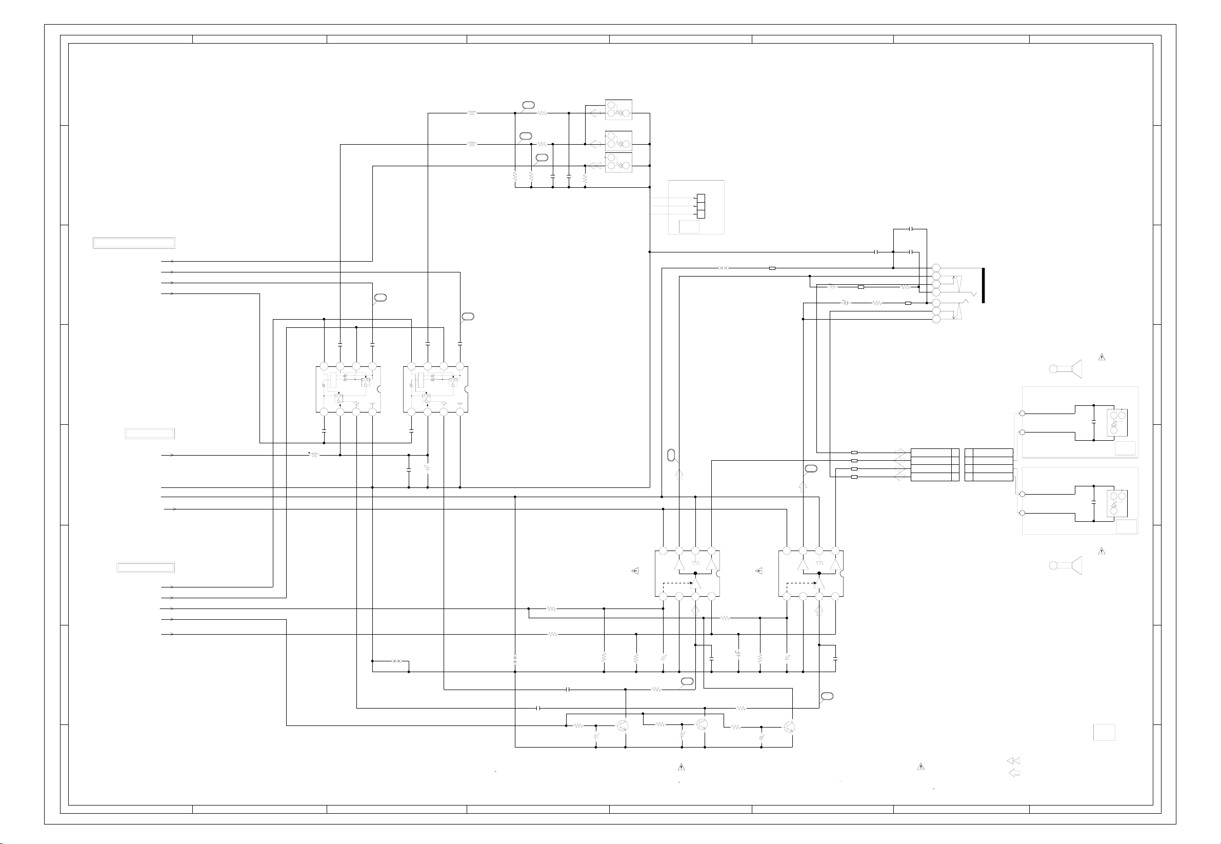
SOUND/AV SCHEMATIC DIAGRAM
47K
R723
820
R721
820
31
C714
0.001 B
(MAIN PCB)
23
HNC
NC
3
2
HNC
NC
3
2
HNC
75
C715
B
0.001
R701
E
1
E
1
E
1
FRONT JACK
RCA JACK(RED)
J703
MTJ-032-05A-31-FE
RCA JACK (WHITE)
J702
MTJ-032-05A-32-FE
RCA JACK (YELLOW)
J704
MTJ-032-05A-30-FE
IMSA-6035B-03Z002-PT1
PCBDB0
CEE093
CP701
8
7
1
2
3
C1019
YK
C1013
25V
47
0.001 B
B1006
W4BRH3.5X6X1.0
R1008
YK
47
W821
B1008
W5RH3.5X5X1.0
C1014
4725V
1/2W
C1015
0.0056 B
C1016
0.0056
B
R1009_1
47 1/2W
B1007
W4BRH3.5X6X1.0
1
5
4
3
2
6
7
HEADPHONE_JACK
J1001
MSJ-2000_AG
6
8
R722
29
30
47K
R712
L707
10uH
L708
10uH
FRONT_VIDEO_IN
7
AV2_A_IN_L
AV2_A_IN_R
FROM/TO CHROMA/SIF/VIF/21PIN
FRONT_VIDEO_IN
6
SCART_AUDIO_R
SCART_AUDIO_L
TUNER_AUDIO
33
SCART_AUDIO_L
SCART_AUDIO_R
32
1F
10016V YK
C712
1F
4.74.84.6
1234
BUFFER
W803
C1002_1
0.022 B
R1001
56K
R1003
47K 1/4W
C1001_1
0.022
B
R1012
39K
C1011
R1004
CP1001
B1001
26
28
5678
08.2 3.5 3.4
5678
08.2 3.5 3.4
-+
IC1001 AN7513
SOUND AMP IC(Rch)
KA
56K
R1005
0.6
0.6
MUTE
Q1001
2250V
2SC2412K
0
KA
100K
R1010
470K
R1013
39K
C1003
1/4W
4.750V
C1012
1234
0
3.95.1 0.3
R1002
1/4W
56K
B
C1005_1
C1004
0.001
25
R1011
MUTE
Q1002
2SC2412K
R1014
33K
470K
0.6
0.6
KA
0
2250V
KA
0.4750V
R1006
C1017
IC1002 AN7513
SOUND AMP IC(Lch)
56K
4.750V KA
C1007
0.6
0.6
MUTE
Q1003
0.4750V
2SC2412K
0
KA
0
27
W4BRH3.5X6X1.0
B1003 W4BRH3.5X6X1.0
W4BRH3.5X6X1.0
B1004
B1005 W4BRH3.5X6X1.0
-+
1234
3.95.1 0.3
C1008
0.001 B
A2502WV2-4P
R
JACK R
JACK L
L
1
2
3
4
CD1001
CH145901
1
2
3
4
R
JACK R
JACK L
L
S1150
R
S1151
JACK R
S1152
L
S1153
JACK L
SPEAKER
NP-300W-L(RCA 115)
C1150
J1151
C1151
SPEAKER
NP-300W-L(RCA 115)
SP1001
8 OHM
J1150
(WHITE)
MTJ-032-05A-32-FE
NC
HNC
2
3
0.001 B
1
E
PCB260
CEE091
(RED)
MTJ-032-05A-31-FE
NC
HNC
2
3
0.001 B
1
E
PCB260
CEE090
SP1002
8 OHM
PCB010
CME049
5
4
3
2
1F
C706
4.8
5
BAIAS
IC701 NJM2534V
TUNER/AV1/AV2 Lch SW
5678
5.2 9.1 0
FROM TV POWER
P.CON+8V
L701
47uH 0305
C705
1F
C707
1F
4.74.84.6
1234
BUFFER
4
GND
SOUND_GND
SOUND+B
3
FROM MICON/TUNER
AV2
AV1
VOLUME
AUDIO_MUTE
POWER
C711
4.8
BAIAS
NJM2534V
IC702
5678
TUNER/AV1/AV2 Rch SW
5.2 9.1 0
C709
1F
C710
C716
0.1 B
W808
2
1
NOTE:THE DC VOLTAGE AT EACH PART WAS MEASURED
WITH THE DIGITAL TESTER WHEN THE COLOR BROADCAST
WAS RECEIVED IN GOOD CONDITION AND PICTURE IS NORMAL.
NOTE:THIS SCHEMATIC DIAGRAM IS THE LATEST AT THE TIME
OF PRINTING AND SUBJECT TO CHANGE WITHOUT NOTICE
CAUTION
:SINCE THESE PARTS MARKED BY
CRITICAL FOR SAFETY,USE ONES
DESCRIBED IN PARTS LIST ONLY
ARE
ATTENTION
:LES PIECES REPAREES PAR UN ETANT
DANGEREUSES AN POINT DE VUE SECURITE
N’UTILISER QUE CELLS DECRITES
DANS LA NOMENCLATURE DES PIECES
TUNER VIDEO SIGNAL
AUDIO SIGNAL
1
ABC D E F GH
G-6G-5
Page 24
8
FROM/TO CHROMA/SIF/VIF/21PIN
G.OUT
R.OUT
B.OUT
VAMP
V_OUT
ABCL
H_OUT
7
6
FROM MICON/TUNER
PROTECT
5
FROM TV POWER
4
P.CON+8V
H.DRV+B
3
ABC DEF GH
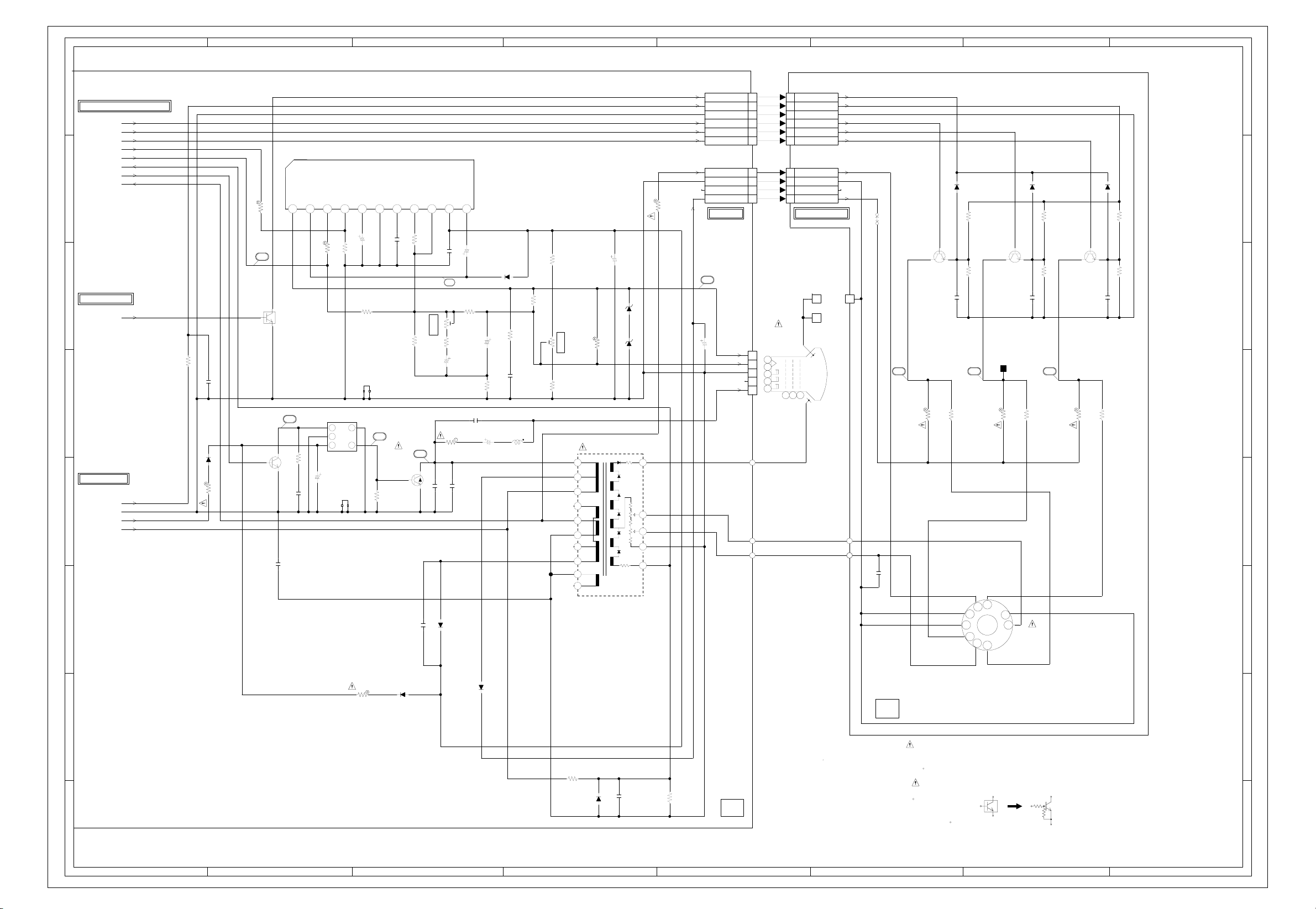
(MAIN PCB)
9
10
8
6
11
FOCUS
SM2041-007
V801
R
G
B
CP802B
B2013H02-6P
1
PROTECT
2
CUT OFF
3
4
G.OUT
5
R.OUT
6
B.OUTB.OUT
CP803B
B2013H02-4P
1
2
3
4
CD801
175
CP802A
B2013H02-6P
CP803A
B2013H02-4P
TO CRT FROM DEFLECTION
36
YK
22
250V
1
PROTECT
2
CUT OFF
3
GND
4
G.OUT
5
R.OUT
6
1
HEATER
2
GND GND
3
NC
4
180V
A34JXV70X73N45A
CP401
A1561WV2-A5P
5
4
3
2
NC
1
ANODE
SCREEN
GND
HEATER
180V
1
1
(to CP001)
CP801
003P-2100
FOCUS
CP806_1
SCREEN
8
GND
NCNCNC
W815
GREEN OUT
2SC1473A
1
41 40
D807
1SS133
1/4W
R809
4.7K
Q801
100.6 2.7
C804
R813
B
390P
2SC1473A
330
RED OUT
Q802
TP023
98.4
D808
1SS133
R811
4.7K 1/4W
R815
390P B
BLUE OUT
Q803
2SC1473A
330
42
3.23.2
2.7
C805
95.4
D809
1SS133
R814
4.7K 1/4W
3.2
2.7
330
R816
C806
390P B
7
6
5
R803
1/4W
R802
15K 1W
2.7K
R805
R804
15K 1W
2.7K 1/2W
R807
1/4W
R806
15K 1W
2.7K
4
0.0012KV B
C819
96.4
6.4
3
4
101.6
0
5
0
6
7
0
0
1
F
J801
8
9
99.6
ISMS01S
3
AFC
GND
DEFLECTION/CRT SCHEMATIC DIAGRAM
PROTECT1 PROTECT1
CUTOFF CUTOFF
GND GND
G.OUT G.OUT
R.OUT R.OUT
B.OUT B.OUT
IC401 TDA8174AV-DRIVE IC
HEATER HEATER
180V 180V
MTZJ27B
MTZJ27B
HV
F
S
GND
11
7
25.2
5.6
R429_1
0
3W
4.7
C448
POWER OUTPUT
OUTPUT STAGE Vs
TRIGGER INPUT
C446
R408
2250V YK
HEIGHT ADJ.
R405
1K +-1%
T401
ETH09K14BZ
34
2
1
HS67
HS402
763WSA0017
R404
0
R422
330 1/4W
C405
1B
D406
11E1-EIC
180 1W
R424
+B
0.3
H.DRIVE
Q402
2SC1627_Y
1101123456789
14.5 23.0 5.0 6.4 4.4 12.0 12.0 4.4 25.0 1.70.0
330K M+-1%
34
2.2
PROTEC
Q403
DTC114EKA
0
37
27.0
1/2W
R446
330
0
MMTS
0.01100V
C440
CH
C401
0.001
Vref. DECOUP.
10
C408
25V KA
390K M+-1%
R406
6.8K1/4W
HS51
HS401
763WSAA016
6
38
R427
GND
100 1/4W
C412
H.OUTPUT
Q401
2SC5885
RAMP GENERATOR
BUFFER OUTPUT
R412
8.2K 1/4W
0.047 MMTV
R417
3.3K 1/4W
39
131.7
0
0
C444
C411
0.0015500V B
Vs
INVERTING INPUT
C413
C414
0.1 B
35
R420
10K1/4W
VR420
470
V_LIN
METAL
1.2K
R419
1050V YK
C417
R447
681/2W
MPP
MPP
0.0082
C443
470P
1.25KV
1.25KV
D405
AU02A-EIC
FB. GENERATOR
10035V YK
YK
2200
C418_1
R407
1.2 1/2W
C437
PMS
0.39250V
C423
2.2250V MHE
D403
11E1-EIC
R416
25V
C422
4.7mH
L401
1 1/2W
MKT
0.15
100V
0909
R410
1/2W
1K
R402
R403
680 1/2W
V_POSI
680 1/4W
6.3
VR401
130
135
NC
NC
NC
METAL
R409
2.2K
FB401 FNI14B002_M
COL
1
0
E180
6
B+
2
0
AFC
9
HEA
TER
10
0
GND
8
0
E12
4
0
E27
3
0
GND
8
0
E8
5
1K +-1%
C403
47035V YK
D401
D402
ABL
R411
1502W
2
1
D407
11E1-EIC
D410
AU02A-EIC
220K
R445
1/4W
D414
C435
11E1-EIC
0.1100V MKT
R421
47K 1/4W
PCB010
CME049
PCB110
CCE042
ATTENTION
CAUTION
NOTE:THIS SCHEMATIC DIAGRAM IS THE LATEST AT THE TIME
:LES PIECES REPAREES PAR UN ETANT
DANGEREUSES AN POINT DE VUE SECURITE
N’UTILISER QUE CELLS DECRITES
DANS LA NOMENCLATURE DES PIECES
:SINCE THESE PARTS MARKED BY
CRITICAL FOR SAFETY,USE ONES
DESCRIBED IN PARTS LIST ONLY
OF PRINTING AND SUBJECT TO CHANGE WITHOUT NOTICE
THE RESISTOR MARKED F IS FUSE RESISTOR.NOTE:
THE ALUMI ELECTROLYTIC CAPACITOR MARKED NP
IS NON POLAR ONE.
ARE
NOTE:THE DC VOLTAGE AT EACH PART WAS MEASURED
WITH THE DIGITAL TESTER WHEN THE COLOR BROADCAST
WAS RECEIVED IN GOOD CONDITION AND PICTURE IS NORMAL.
CAUTION: DIGITAL TRANSISTOR
2
1
ABC DEF GH
G-8G-7
Page 25
ABC DEF GH
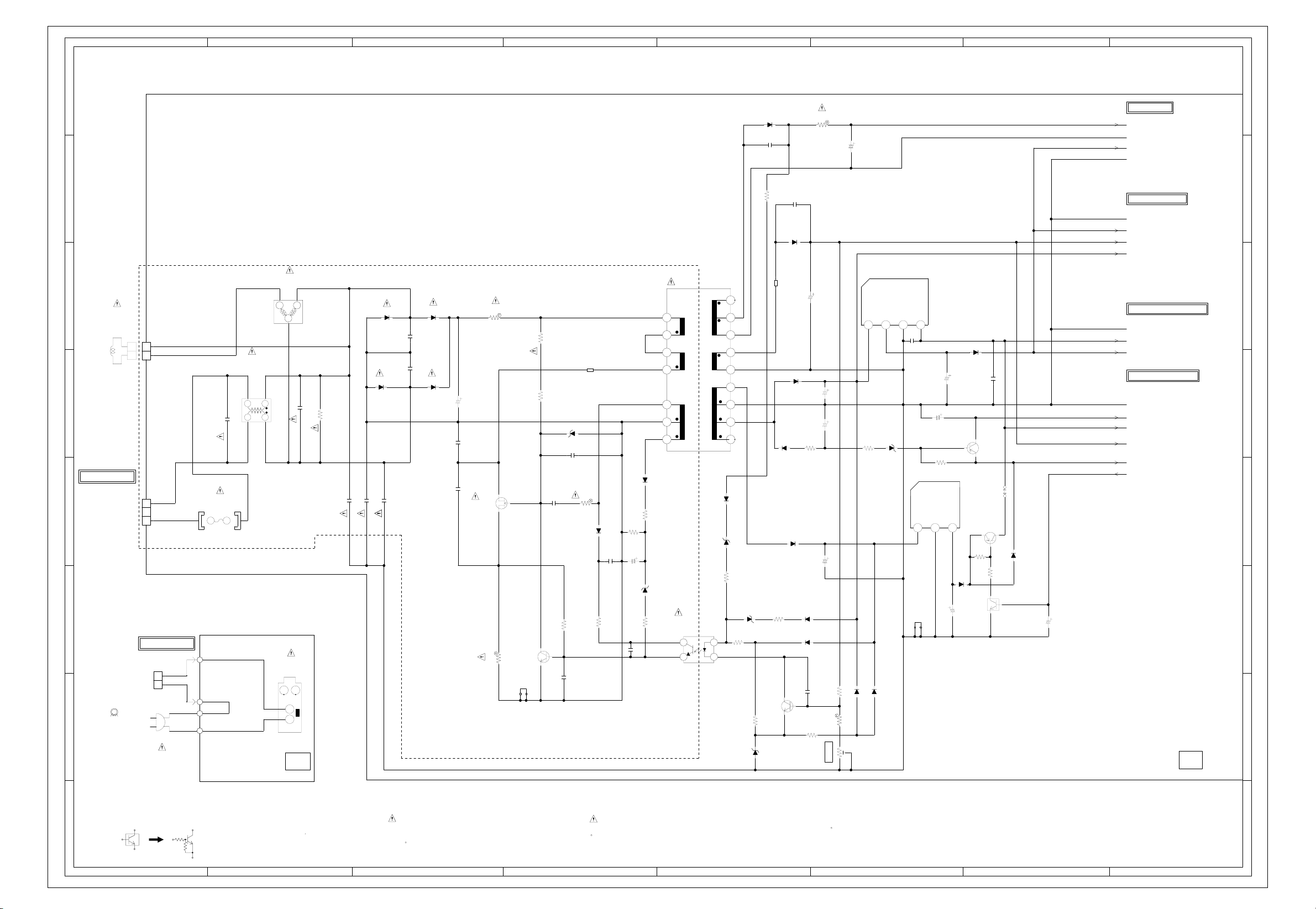
TV POWER SCHEMATIC DIAGRAM
8
(MAIN PCB)
8
7
TH501
B59104-T80-B10
6
DEGAUSS COIL
L503
8R140018
21
CP502
A1561WV2-2PK
1
2
COIL LINE FILTER
0R7A223F24Y
5
C501
0.22275V ECQUL
FROM/TO POWER SW
CP503
A3963WV2-3PD
4
POWER_SW SCHEMATIC DIAGRAM
3
BLUE
12
BROWN
FH501
EYF-52BCY
F501
50T040H
T4A_L_250V
EYF-52BCY
FH502
PH
L501
34
12
(POWER_SW PCB)
FROM/TO MAIN
CD503
CHU23001
1
2
2
L502
W5T_20X10X10A
AC230V_50Hz
CD501_1
06455821
BLUE
BROWN
S503B
BROWN
S503A
BLUE
S501A
BLUE
S501B
BROWN
MAIN POWER SW
SW501
ESB92S22B
3 4
NCNC
1
2
PW/SW
CEE102
123
C502
0.22275V ECQUL
R501
1.5M 1/2W
C532
0.001250V KX
RM11C-EIC
C528
D503
RM11C-EIC
D504
KX
C527
470P250V
0.0015
250V KX
C503
C504
D501
B
RM11C-EIC
0.0022
2KV
0.0022
D502
2KV B
RM11C-EIC
82400V USR
C505
680P2KV R
C509
C507
0.00122KV R
2SK2647-01MR
POWER
Q501
R503
0.22 1W
R516
237.7
D
G
S
0.3
1W
1
763WAA0162
6.7
POWER
Q502
KTC3203_Y
HS9V
HS501
R520
1.5M 1/2W
R517
1.5M 1/4W
C516
0.047MMTV
6.7
0
0.0047
R511
0.3
C524
MTZJ18B
C526
B501
W4BRH3.5X6X1.0X2
D522
B
R502
2201W
D505
0.47
1/4W
R510
680
0.0033 B
1SS133
C518_1
2.2K 1/4W
MMTS
R525
2.2K
1/4W
C519
50V
C531
TO SOUND/AV
SOUND+B
SOUND_GND
P.CON+8V
GND
D527
21DQ09N
C534
470P500V B
R530_1
1.5 1W
C535
47016V YK
7
C517_1
R504
1K 1/4W
0.0012KV RR
D510
RU2AM-EIC
REG.9V IC
T501 8129110H
258.8
8
270
7
270
6
237.7
5
45.9
3
0
2
19.1
1
D507
1SS133
R523
220 1/4W
1
KA
D508
MTZJ18B
FEED BACK
R522
IC504
2.2K
LTV-817M-VB
12.3
B
0.001
0.3
34
1
9.1
2
8.1
D515
D529
R529
0
NC
10
0
11
0
12
163.9
13
0
14
0
15
13.0
16
9.7
17
0
18
NC
1SS133
MTZJ5.6B
100 1/4W
MTZJ3.6B
R512
4701/4W
D524
FEED BACK
SWITCHING
KTC3198
R513
D528
B504
1N4937
R532
1K
Q507
560 1/4W
MTZJ5.6B
C521
W4BRH3.5X6X1.0X2
D513
21DQ09N
R526
D511
1001/4W
D516
21DQ09N
D523
1SS133
D518
1SS133
C513
8.1
6.2
5.6
R519
1001/4W
100160V YXF
470
C515
16V
C506
0.4750V KA
C522
100016V YK
R514
0.01 B
R518
+B ADJ
IC503 KIA78R09API
1234
YK
R507
2.2K
D514
D521
56K 1/2W
1SS133
M+-1%
2.2K
1K
VR501
11.2
OUTINGND
8.0
D525
MTZJ12B
1SS133
SW
0
5.0
C529
0.001
B
C533
10
25V KA
R508 10K
REG.6V IC
IC502 KIA7806API
GND
IN
123
HS6S
HS502
763WAAA048
C525
6.008.0
C508
11E1-EIC
22016V YK
4.2
OUT
D509
11E1-EIC
P.CON SW
10010V YK
DTC124EKA
D517
4.9
4.9
Q510
P.FAIL
2SA1037AK
P.CON SW
Q511
KTA1281_Y
5.1
R515
10K
R524
C530
Q506
B
0.001
W825
5.0
4.4
D512
SB140-EIC
560 1/4W
0.1
4.7
0
C514
1025V KA
TO DEFLECTION/CRT
GND
P.CON+8V
+B
H.DRV+B
TO CHROMA/SIF/VIF/21PIN
GND
P.CON+5V
P.CON+8V
FROM/TO MICON/TUNER
GND
POWER_FAIL
P.CON+5V
+B
AT+5V
POWER
PCB010
CME049
6
5
4
3
2
1
CAUTION: DIGITAL TRANSISTOR
ATTENTION
:LES PIECES REPAREES PAR UN ETANT
DANGEREUSES AN POINT DE VUE SECURITE
N’UTILISER QUE CELLS DECRITES
DANS LA NOMENCLATURE DES PIECES
CAUTION
:SINCE THESE PARTS MARKED BY
CRITICAL FOR SAFETY,USE ONES
DESCRIBED IN PARTS LIST ONLY
ARE
NOTE:THIS SCHEMATIC DIAGRAM IS THE LATEST AT THE TIME
OF PRINTING AND SUBJECT TO CHANGE WITHOUT NOTICE
NOTE:THE DC VOLTAGE AT EACH PART WAS MEASURED
WITH THE DIGITAL TESTER WHEN THE COLOR BROADCAST
WAS RECEIVED IN GOOD CONDITION AND PICTURE IS NORMAL.
1
ABC DEF GH
G-10G-9
Page 26
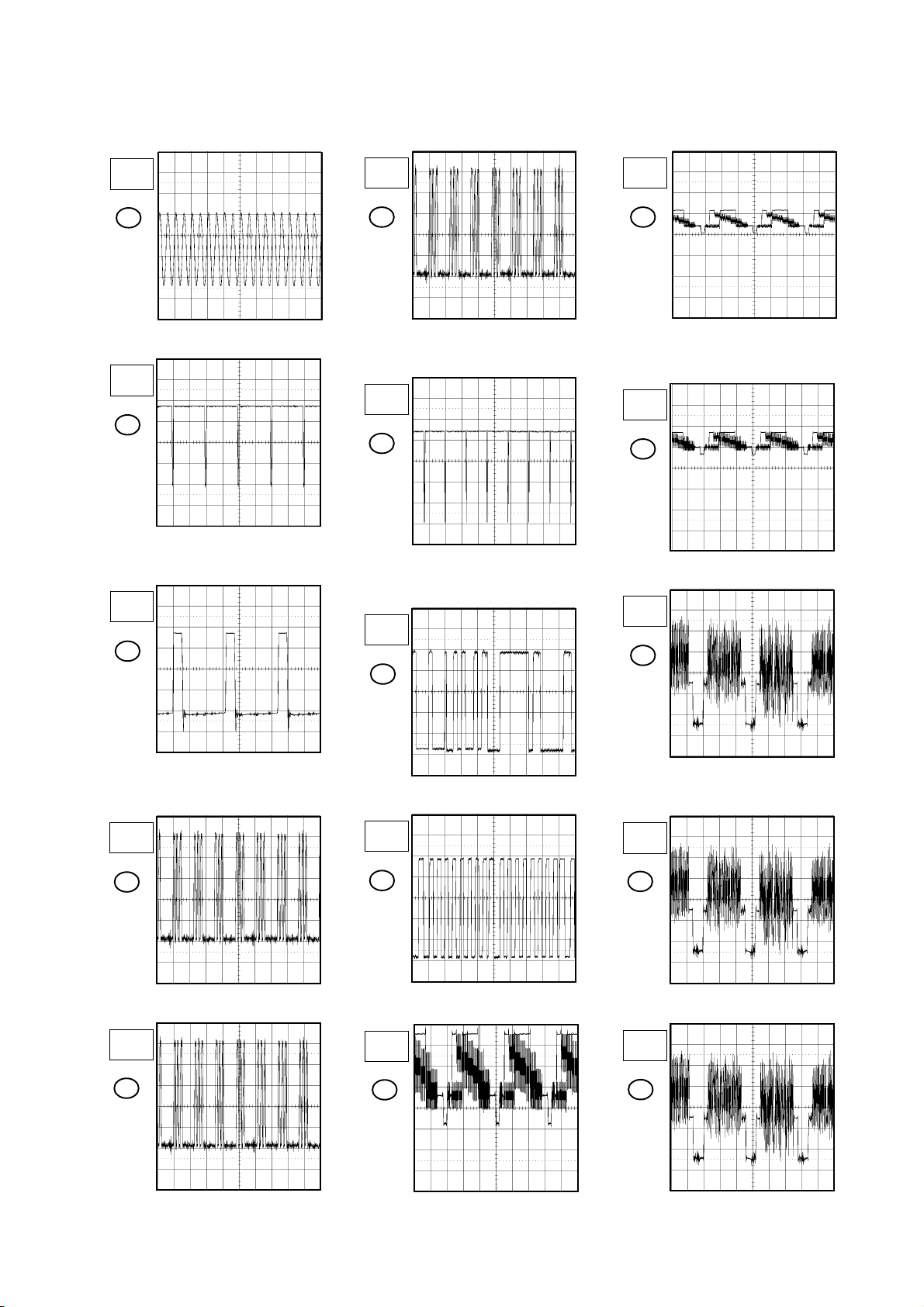
MICON/TUNER
WAVEFORMS
0.5µs
1V
1
10ms
1V
2
20µs
1V
3
50µs
100mV
7
50µs
0.5V
8
0.2ms
1V
9
20µs
1V
13
20µs
1V
14
20µs
100mV
16
50µs
100mV
5
50µs
100mV
6
0.2ms
1V
10
20µs
1V
17
CHROMA/SIF/VIF/21PIN
20µs
0.5V
11
The following waveforms were measured at the point of the corresponding
NOTE:
balloon number in the schematic diagram.
H-1
20µs
100mV
18
Page 27
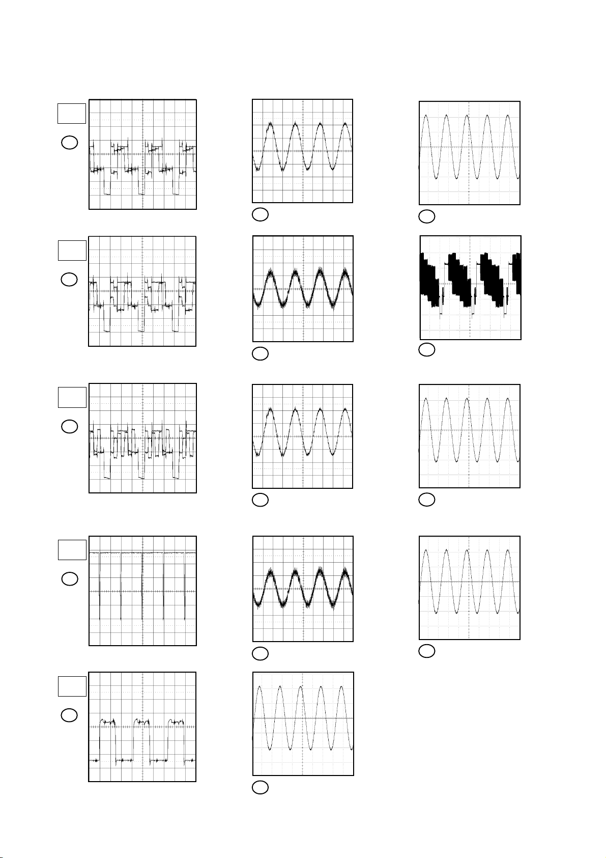
20µs
1V
19
WAVEFORMS
SOUND/AV
20µs
1V
20
20µs
1V
21
25 200mV 1ms/div
26
0.5V 1ms/div
27 200mV 1ms/div
200mV 500µs/div
30
31 500mV 20µs/div
200mV 500µs/div
32
10ms
1V
23
20µs
200mV
24
200mV 500µs/div
28
0.5V 1ms/div
200mV 500µs/div
29
The following waveforms were measured at the point of the corresponding
NOTE:
balloon number in the schematic diagram.
33
H-2
Page 28
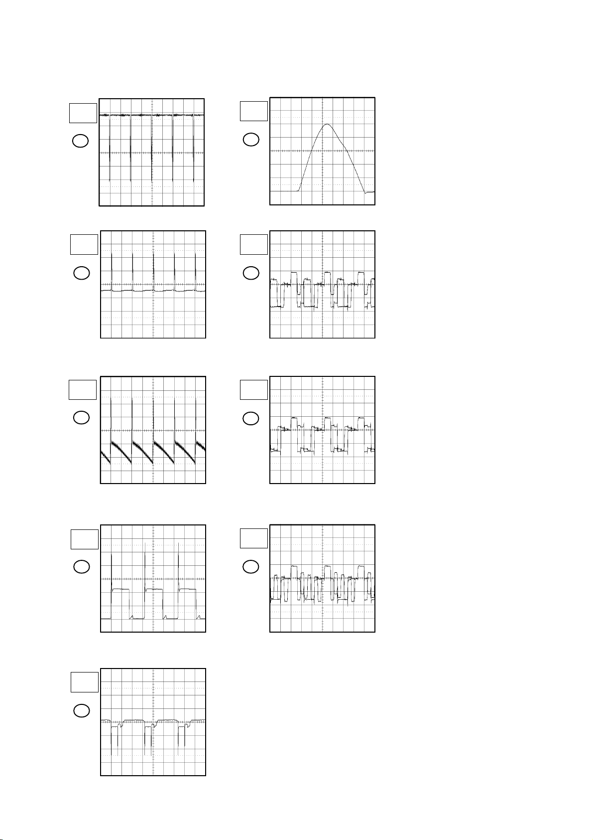
DEFLECTION/CRT
10ms
1V
WAVEFORMS
2µs
200V
34
10ms
10V
35
10ms
10V
36
39
20µs
50V
40
20µs
50V
41
20µs
10V
37
20µs
5V
38
20µs
50V
42
The following waveforms were measured at the point of the corresponding
NOTE:
balloon number in the schematic diagram.
H-3
Page 29
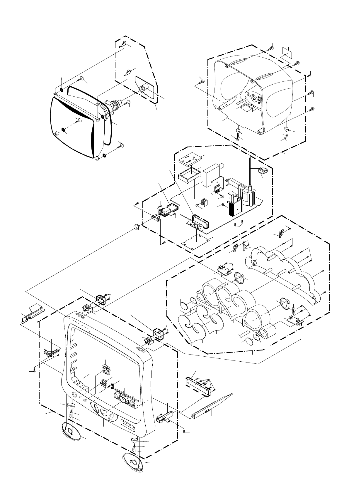
MECHANICAL EXPLODED VIEW
114
205
108
205
115
V801
206
115
206
115
114
206
PCB110
(CRT PCB ASS'Y)
L503
206
PCBDB0
115
(RELAY PCB ASS'Y)
PCB320
(POWER SW PCB ASS'Y)
202
103
113
202
202
J801
202
205
107
207
109
203
207
106
102A
102D
116M
207
204
202
102B
201
202
116K
112
116L
201
102D
202
205
205
102C
102
PCB010
(MAIN PCB ASS'Y)
202
202
202
202
110
202
101
PCB260A
(FRONT JACK PCB ASS'Y)
101G
202
101B
201
101I
104
205
PCB260B
(FRONT JACK PCB ASS'Y)
101K
101F
101D
101J
101E
101A
101L
201
101I
202
101C
105
116G
205
101H
202
116I
116F
116C
116E
116B
PCB270
(OPERATION PCB ASS'Y)
202
111
202
116A
116G
116D
SP1002
116F
116
116H
SP1001
202
116N
202
116J
I-1
Page 30
MECHANICAL REPLACEMENT PARTS LIST
REF. NO. PART NO. DESCRIPTION
101 7A701A567A FRONT CABI ASS'Y
101A 701WPJD162 CABINET,FRONT
101B 704WPAA029 LEG-FRONT(L)
101C 704WPAA030 LEG-FRONT(R)
101D 713WPAA174 GUIDE REMOCON
101E 738WPJA023 BUTTON FRAME-PRINCESS
101F 738WPBA132 BUTTON,FRAME
101G 761WPAA096 HOLDER,PCB-2(L)
101H 761WPAA097 HOLDER PCB-2(R)
101I 800WFA0060 CUSHION LEG
101J 713WPAA175 GLASS LED
101K 761WPAA133 HOLDER,SPEAKER-PCB(L)
101L 761WPAA134 HOLDER,SPEAKER-PCB(R)
102 7A702A172A BACK CABI ASS'Y
102A 702WPBA206 CABINET BACK
102B 704WPAA027 LEG-BACK(L)
102C 704WPAA028 LEG-BACK(R)
102D 800WFA0060 CUSHION LEG
103 735WPAA782 HOLDER,POWER SW
104 704WPAA031 LEG,PRINCESS(L)
105 704WPAA032 LEG,PRINCESS(R)
106 752WSAA006 PLATE,SHIELD
107 752WSAA008 SHIELD,CASE
108 722616A031 SHEET RATING
109 752WSAA013 SHIELD,LID
110 761WPAA107 HOLDER,PCB (L)
111 761WPAA108 HOLDER,PCB (R)
112 899HV3T000 HOLDER ANODE WIRE
113 735WPBB239 BUTTON,POWER
114 8994101000 HOLDER CRT WIRE
115 800WR0A011 SHEET CRT SUPPORT (D)
116 7A701A568A SPEAKER CABI ASS'Y
116A 701WPBA062 CABINET FRONT-SP
116B 711WPAA116 PLATE,HEART-CENTER
116C 711WPAA117 PLATE,HEART(L)
116D 711WPAA118 PLATE,HEART(R)
116E 729WDAA001 DUBLE,FACE-TAPE 1
116F 729WDAA002 DUBLE,FACE-TAPE 2
116G 800WQ0A086 FELT SHEET T=0.5
116H 702WPBA205 CABINET BACK SP.1/2
116I 761WPAA109 HOLDER,TIARA(L)
116J 761WPAA110 HOLDER,TIARA(R)
116K 761WPAA111 HOLDER,SPEAKER1(L)
116L 761WPAA112 HOLDER,SPEAKER1(R)
116M 761WPAA113 HOLDER,SPEAKER2(L)
116N 761WPAA114 HOLDER,SPEAKER2(R)
201 8117330A0U SCREW TAPPING(BO) FLAT 3x10
202 8110630A0U SCREW TAP TITE(P) BRAZIER 3x10
203 810763080U SCREW TAP TITE(S) BRAZIER 3x8
204 810963080Q SCREW TAP TITE(B) BRAZIER 3x8
205 8117540A6U SCREW TAP TITE(B0) TRUSS 4x16
206 8121J50B5U SCREW TAP TITE(P) GW20 5x28
207 8109I3080U SCREW TAP TITE(B) WH7 3x8
--- 793WCDC966 GIFT BOX
--- 791WHAA122 FILM BAG
--- 791WHAA137 LIGHTRON SHEET
--- 792UHAA057 PACKAGE,BOTTOM
--- 792UHAA064 PACKAGE,TOP
--- A3Q909W975 INSTRUCTION BOOK KIT
--- J3Q90502A GUARANTEE CARD
--- J3Q909B1A INSTRUCTION BOOK
--- JA4XD200 POLYBAG,INSTRUCTION(RED CAUTION)
J1-1
Page 31
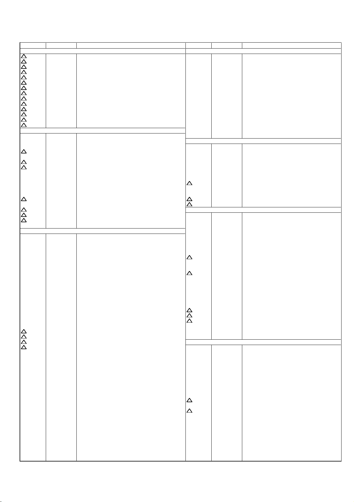
ELECTRICAL REPLACEMENT PARTS LIST
REF. NO. PART NO. DESCRIPTION REF. NO. PART NO. DESCRIPTION
RESISTORS DIODES
! R408 R4X5T6102F R,METAL 1K OHM 1/6W D602 D1VT001330 DIODE,SILICON 1SS133T-77
! R411 R3X28A151J R,METAL OXIDE 150 OHM 2W D603 D1VT001330 DIODE,SILICON 1SS133T-77
! R424 R3X181181J R,METAL OXIDE 180 OHM 1W D604 D2WT011E10 DIODE SILICON 11E1-EIC
! R429 R3X28B4R7J R,METAL OXIDE 4.7 OHM 3W D606 D97U06R81B DIODE,ZENER MTZJ6.8B T-77
! R447 R638U2680J R,FUSE 68 OHM 1/2W D607 D97U06R81B DIODE,ZENER MTZJ6.8B T-77
! R501 R002T2155J RC 1.5M OHM 1/2W D608 D97U06R81B DIODE,ZENER MTZJ6.8B T-77
! R502 R3X181221J R,METAL OXIDE 220 OHM 1W D609 D97U05R61B DIODE,ZENER MTZJ5.6B T-77
! R503 R63881R22J R,FUSE 0.22 OHM 1W D610 D97U09R11B DIODE,ZENER MTZJ9.1B T-77
! R516 R3X181010J R,METAL OXIDE 1 OHM 1W D611 D97U05R61B DIODE,ZENER MTZJ5.6B T-77
! R520 R002T2155J RC 1.5M OHM 1/2W D703 D97U05R61B DIODE,ZENER MTZJ5.6B T-77
! R530 R3X1811R5J R,METAL OXIDE 1.5 OHM 1W D705 D97U05R61B DIODE,ZENER MTZJ5.6B T-77
! R803 R3X181153J R,METAL OXIDE 15K OHM 1W D706 D97U05R61B DIODE,ZENER MTZJ5.6B T-77
! R805 R3X181153J R,METAL OXIDE 15K OHM 1W D709 D97U05R11B DIODE,ZENER MTZJ5.1B T-77
! R807 R3X181153J R,METAL OXIDE 15K OHM 1W D807 D1VT001330 DIODE,SILICON 1SS133T-77
CAPACITORS
C418 E02L03222M CE 2200 UF 25V D809 D1VT001330 DIODE,SILICON 1SS133T-77
C437 P4J7F3394J CMPP 0.39 UF 250V PMS
C443 P4N8FJ822H CMPP 0.0082UF 1.25KV IC101 I56D07110A IC OEC7110A
! C444 P4N8FJ471J CMPP 470 PF 1.25KV IC102 I9UF032310 IC PST3231NR
C448 E0ELFD220M CE 22 UF 250V IC199 A3Q907W015 INIT DATA
! C501 P2122B224M CMP 0.22 UF 275V ECQUL IC201 I0WDE2248H IC STV2248H
! C502 P2122B224M CMP
C503 C0JBB07H3K CC 0.0022UF 2KV B IC502 I1KA97806A IC KIA7806API
C504 C0JBB07H3K CC 0.0022UF 2KV B IC503 I1KA98R09A IC KIA78R09API
C505 E52DHH820M CE 82 UF 400V ! IC504 0002E00610 PHOTO COUPLER LTV-817M-VB
C507 C03L0R7B3K CC 0.0012UF 2KV R IC701 I0QF02534V IC NJM2534V(TE2)
C509 C0PLRR7U2K CC 680 PF 2KV R IC702 I0QF02534V IC NJM2534V(TE2)
! C517 C0PLRR713K CC 0.001 UF 2KV R ! IC1001 I01DP75130 IC AN7513
C521 E62NFB101M CE 100 UF 160V ! IC1002 I01DP75130 IC AN7513
! C527 CD39E0ME3M CC 0.0015UF 250V
! C528 CD39B0MQ2K CC 470 PF 250V Q103 T6YJ1037K0 TRANSISTOR,SILICON 2SA1037AKT146R,S
! C532 CD39E0M13M CC 0.001 UF 250V Q201 T8AA03881S TRANSISTOR SILICON KTC3881S-RTK
C819 C0JBB0713K CC 0.001 UF 2KV B Q203 TCATC31980 TRANSISTOR,SILICON KTC3198-AT(Y,GR)
0.22 UF 275V ECQUL IC401 I0WTD81740 IC TDA8174A
DIODES
D001 D97U03301B DIODE,ZENER MTZJ33B T-77 Q301 T8AA03881S TRANSISTOR SILICON KTC3881S-RTK
D101 0021721150 LED SLR-342VCT32 Q302 T8AA03881S TRANSISTOR SILICON KTC3881S-RTK
D102 D97U05R61B DIODE,ZENER MTZJ5.6B T-77 Q303 T8YJ2412K0 TRANSISTOR SILICON 2SC2412KT146 R,S
D103 D97U05R11B DIODE,ZENER MTZJ5.1B T-77 Q304 TNYJC05001 COMPOUND TRANSISTOR DTC124EKAT146
D104 D1VT001330 DIODE,SILICON 1SS133T-77 ! Q401 TC1G058850 TRANSISTOR SILICON 2SC5885
D105 D1VT001330 DIODE,SILICON 1SS133T-77 Q402 TC5T01627Y TRANSISTOR SILICON 2SC1627_Y(TPE2)
D106 D97U05R61B DIODE,ZENER MTZJ5.6B T-77 Q403 TNYJB05001 COMPOUND TRANSISTOR DTC114EKAT146
D107 D97U05R61B DIODE,ZENER MTZJ5.6B T-77 ! Q501 T410K26470 FET 2SK2647-01MR
D109 D97U05R61B DIODE,ZENER MTZJ5.6B T-77 Q502 TCAT032034 TRANSISTOR, SILICON KTC3203_Y-AT
D301 DD1R0MA770 DIODE,SILICON MA77 Q506 T6YJ1037K0 TRANSISTOR,SILICON 2SA1037AKT146R,S
D401 D97U02701B DIODE,ZENER MTZJ27B T-77 Q507 TCATC31980 TRANSISTOR,SILICON KTC3198-AT(Y,GR)
D402 D97U02701B DIODE,ZENER MTZJ27B T-77 Q510 TNYJC05001 COMPOUND TRANSISTOR DTC124EKAT146
D403 D2WT011E10 DIODE SILICON 11E1-EIC Q511 TAAT01281Y TRANSISTOR SILICON KTA1281_Y
D405 D2WTAU02A0 DIODE SILICON AU02A-EIC Q605 T8YJ2412K0 TRANSISTOR SILICON 2SC2412KT146 R,S
D406 D2WT011E10 DIODE SILICON 11E1-EIC ! Q801 TCKT1473A0 TRANSISTOR SILICON 2SC1473A-TA-(RQ)
D407 D2WT011E10 DIODE SILICON 11E1-EIC ! Q802 TCKT1473A0 TRANSISTOR SILICON 2SC1473A-TA-(RQ)
D410 D2WTAU02A0 DIODE SILICON AU02A-EIC ! Q803 TCKT1473A0 TRANSISTOR SILICON 2SC1473A-TA-(RQ)
D414 D2WT011E10 DIODE SILICON 11E1-EIC Q1001 T8YJ2412K0 TRANSISTOR SILICON 2SC2412KT146 R,S
! D501 D2WTRM11C0 DIODE SILICON RM11C-EIC Q1002 T8YJ2412K0 TRANSISTOR SILICON 2SC2412KT146 R,S
! D502 D2WTRM11C0 DIODE SILICON RM11C-EIC Q1003 T8YJ2412K0 TRANSISTOR SILICON 2SC2412KT146 R,S
! D503 D2WTRM11C0 DIODE SILICON RM11C-EIC
! D504 D2WTRM11C0 DIODE SILICON RM11C-EIC L001 02167F100J COIL 10 UH
D505 D1VT001330 DIODE,SILICON 1SS133T-77 L101 02167F3R3J COIL 3.3 UH
D507 D1VT001330 DIODE,SILICON 1SS133T-77 L103 021LA6100K COIL 10 UH
D508 D97U01801B DIODE,ZENER MTZJ18B T-77 L202 02167F3R3J COIL 3.3 UH
D509 D2WT011E10 DIODE SILICON 11E1-EIC L203 021LA61R0M COIL 1 UH
D510 D2WXRU2AM0 DIODE SILICON RU2AM-EIC L204 021LA6120K COIL 12 UH
D511 D2WXN49370 DIODE SILICON 1N4937 L206 021LA6R22M COIL 0.22 UH
D512 D2WXSB1400 DIODE SCHOTTKY SB140-EIC L207 033700005R COIL,VIDEO IFT 3700005
D513 D28T21DQN9 DIODE SCHOTTKY 21DQ09N-TA2B1 L302 021LA6R22M COIL 0.22 UH
D514 D1VT001330 DIODE,SILICON 1SS133T-77 L401 021679472K COIL 4.7 MH
D515 D1VT001330 DIODE,SILICON 1SS133T-77 ! L501 029T000094 COIL,LINE FILTER 0R7A223F24Y
D516 D28T21DQN9 DIODE SCHOTTKY 21DQ09N-TA2B1 L502 02AHB0A0A4 CORE FERRITE W5T_20X10X10A
D517 D2WT011E10 DIODE SILICON 11E1-EIC ! L503 028R140018 COIL,DEGAUSS 8R140018
D518 D1VT001330 DIODE,SILICON 1SS133T-77 L601 02167F100J COIL 10 UH
D521 D1VT001330 DIODE,SILICON 1SS133T-77 L701 02167F470J COIL 47 UH
D522 D97U01801B DIODE,ZENER MTZJ18B T-77 L702 021LA6100K COIL 10 UH
D523 D1VT001330 DIODE,SILICON 1SS133T-77 L703 021LA6100K COIL 10 UH
D524 D97U03R61B DIODE,ZENER MTZJ3.6B T-77 L704 021LA6100J COIL 10 UH
D525 D97U01201B DIODE,ZENER MTZJ12B T-77 L706 021LA6100K COIL 10 UH
D527 D28T21DQN9 DIODE SCHOTTKY 21DQ09N-TA2B1 L707 021LA6100K COIL 10 UH
D528 D97U05R61B DIODE,ZENER MTZJ5.6B T-77 L708 021LA6100K COIL 10 UH
D529 D97U05R61B DIODE,ZENER MTZJ5.6B T-77 T401 045009003J TRANS,HORIZONTAL DRIVE ETH09K14BZ
D808 D1VT001330 DIODE,SILICON 1SS133T-77
ICS
AT24C08AN-10SU-2.7
TRANSISTORS
Q204 T8YJ2412K0 TRANSISTOR SILICON 2SC2412KT146 R,S
COILS &TRANSFORMERS
J2-1
Page 32
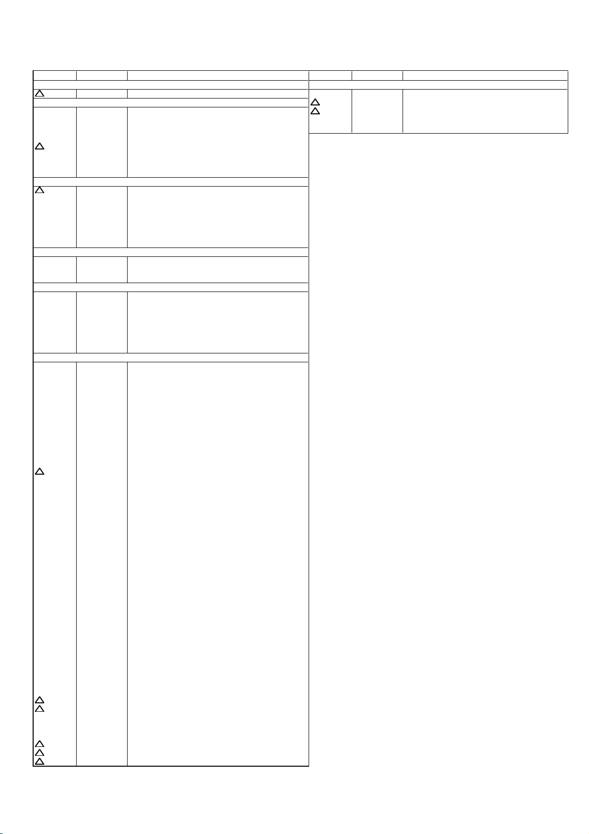
ELECTRICAL REPLACEMENT PARTS LIST
.
REF. NO. PART NO. DESCRIPTION REF. NO. PART NO. DESCRIPTION
COILS &TRANSFORMERS MISCELLANEOUS
! T501 048129110H TRANSFORMER,SWITCHING 8129110H TM101 076N0JP030 TRANSMITTER RC-JP030
JACKS
J701 063D100050 SOCKET,21PIN MRC-021V-07_A ! V801 09FY140402 CRT W/DY(B+D) A34JXV70X73N45A
J702 060J421037 RCA JACK MTJ-032-05A-32-FE X101 100CT8R005 CRYSTAL HC-49/U-S
J703 060J421030 RCA JACK MTJ-032-05A-31-FE X601 100CT4R408 CRYSTAL HC-49/U
J704 060J421036 RCA JACK MTJ-032-05A-30-FE
! J801 066F120018
J1001 060J131016 HEADPHONE JACK MSJ-2000_AG RC................... CARBON RESISTOR
J1150 060J421037 RCA JACK MTJ-032-05A-32-FE
J1151 060J421030 RCA JACK MTJ-032-05A-31-FE CAPACITORS
SOCKET,CATHODE RAY TUBE ISMS01S RESISTOR
SWITCHES
! SW501 0530105019 SWITCH ESB92S22B CE................... ALUMI ELECTROLYTIC CAPACITOR
SW2002 0504101T34 SWITCH,TACT EVQ21505R CP................... POLYESTER CAPACITOR
SW2003 0504101T34 SWITCH,TACT EVQ21505R CPP.................. POLYPROPYLENE CAPACITOR
SW2004 0504101T34 SWITCH,TACT EVQ21505R CPL.................. PLASTIC CAPACITOR
SW2005 0504101T34 SWITCH,TACT EVQ21505R CMP..................
SW2006 0504101T34 SWITCH,TACT EVQ21505R CMPL................ METAL PLASTIC CAPACITOR
SW2007 0504101T34 SWITCH,TACT EVQ21505R CMPP................ METAL POLYPROPYLENE CAPACITOR
! TU001 0145517012 TUNER,VHF-UHF TUWRF4EG-778F2A_P3
CC................... CERAMIC CAPACITOR
METAL POLYESTER CAPACITOR
VARIABLE RESISTORS
VR401 V1K63H3BTE VOLUME,SEMI FIXED NVG6TLTAB222
VR420 V1K63Q2BTE VOLUME,SEMI FIXED NVG6TLTAB471
VR501 V116313BTC VOLUME,SEMI FIXED EVNCYAA03B13
P.C.BOARD ASSEMBLIES
PCB010 A3Q909W010K PCB ASS'Y CME049A
PCB110 A3Q909W110K PCB ASS'Y CCE042A
PCB270 A3Q909W270K PCB ASS'Y CEE092A
PCB320 A3Q909W320K PCB ASS'Y CEE102A
PCBDB0 A3Q909WDB0K PCB ASS'Y CEE093A
PCB260A A3Q909W260K PCB ASS'Y CEE090A
PCB260B A3Q909W260K PCB ASS'Y CEE091A
MISCELLANEOUS
B501 024HT03563 CORE,BEADS W4BRH3.5X6X1.0X2
B504 024HT03563 CORE,BEADS W4BRH3.5X6X1.0X2
B1001 024HT03564 CORE,BEADS W4BRH3.5X6X1.0
B1002 024HT03564 CORE,BEADS W4BRH3.5X6X1.0
B1003 024HT03564 CORE,BEADS W4BRH3.5X6X1.0
B1004 024HT03564 CORE,BEADS W4BRH3.5X6X1.0
B1005 024HT03564 CORE,BEADS W4BRH3.5X6X1.0
B1006 024HT03564 CORE,BEADS W4BRH3.5X6X1.0
B1007 024HT03564 CORE,BEADS W4BRH3.5X6X1.0
B1008 024HT03553 CORE,BEADS W5RH3.5X5X1.0
BT001 141R004016 BATTERY,MANGAN GR03X-SP2
BT002 141R004016 BATTERY,MANGAN GR03X-SP2
! CD501 1206455821 CORD AC BUSH 6455821
CD503 06CHU23001 CORD CONNECTOR CHU23001
CD801 1278140031 BRAIDED WIRE SM2041-007
CD802 WDL6042038 FLAT CABLE
CD803 WBL6028038 FLAT CABLE AWG26 4C BLACK 280MM
CF201 1012T5R515 FILTER,CERAMIC TRAP TPWRF5M50B02-A0
CF202 102E238R9E FILTER,SAW J1981M
CF204 1012T03101 FILTER CERAMIC TRAP MKT31.9MA110P-TF
CF301 102E238R94 FILTER,SAW K9650M
CF304 1012T04001 FILTER,CERAMIC TRAP MKT40.4MA110P-TF
CP001 069W01001A CONNECTOR PCB SIDE 003P-2100
CP101 069S260629 CONNECTOR PCB SIDE A2001WV2-6P
CP102 069S270639 CONNECTOR PCB SIDE A2001WR2-7P
CP401 069S450089 CONNECTOR PCB SIDE A1561WV2-A5P
CP502 069S420099 CONNECTOR PCB SIDE A1561WV2-2PK
CP503 069S320419 CONNECTOR PCB SIDE A3963WV2-3PD
CP701 069J130340 CONNECTOR PCB SIDE
CP801 069W01001A CONNECTOR PCB SIDE 003P-2100
CD1001 06CH145901 CORD CONNECTOR CH145901
CD2001 06CH262003 CORD CONNECTOR CH262003
CP1001 069S140419 CONNECTOR PCB SIDE A2502WV2-4P
CP802A 067U006049 WIRE HOLDER B2013H02-6P
CP802B 067U006049 WIRE HOLDER B2013H02-6P
CP803A 067U004029 WIRE HOLDER B2013H02-4P
CP803B 067U004029 WIRE HOLDER B2013H02-4P
EL002 124120301A EYE LET XRY20X30BD
! F501 080NT04004 FUSE 50T040H
! FB401 043214050F TRANSFORMER,FLYBACK FNI14B002_M
FH501 06710T0009 HOLDER,FUSE EYF-52BCY
FH502 06710T0009 HOLDER,FUSE EYF-52BCY
OS2001 077Q037002 REMOTE RECEIVER PIC-37143TH5
! SP1001 070W132024 SPEAKER
! SP1002 070W132024 SPEAKER NP-300W-L(RCA 115)
! TH501 D8E080B100 DEGAUSS ELEMENT B59104-T80-B10
AWG26 6C BLACK 420MM
IMSA-6035B-03Z002-PT
NP-300W-L(RCA 115)
J2-2
Page 33

SPEC.NO.
O/R NO.
M3Q9-09W
U593562
 Loading...