

Page 1
A
f
Please click here to visit our online spice models database.
Product Line o
200V PNP LOW V
Features
• BV
• BV
• Continuous current I
• V
• R
• P
• 2 Amps continuous current
• Up to 5 Amps peak current
• Very low saturation voltage
• Enhanced switching performance
> -200V
CEO
> -2V
ECO
< -160mV @ -1A
CE(sat
=130mΩ
CE(sat)
= 2.4W
D
C(cont)
= 2A
Mechanical Data
• Case: SOT-89
• UL Flammability Rating 94V-0
• Moisture Sensitivity: Level 1 per J-STD-020
• Terminals: Matte Tin Finish
• Weight: 0.052 grams (approximate)
Diodes Incorporated
TRANSISTOR IN SOT-89
CE(sat)
ZXTP03200BZ
Applications
• DC-DC Convertors
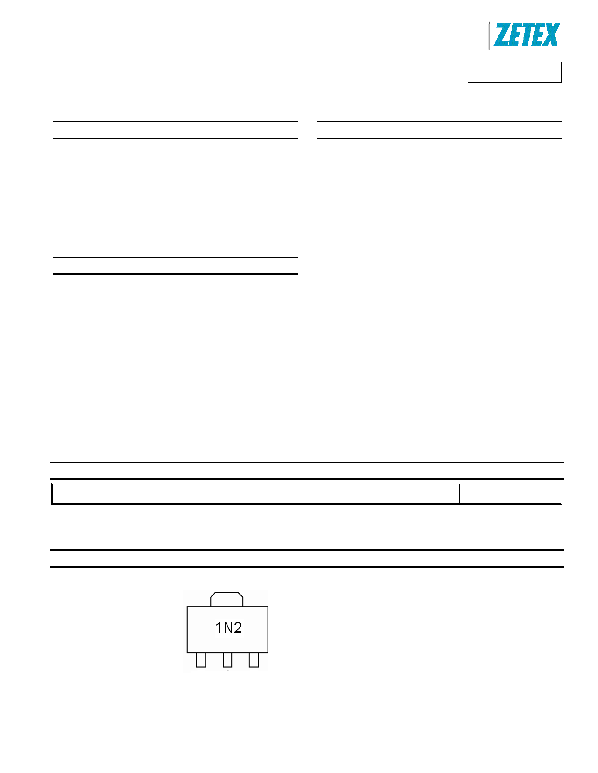
SOT-89
Top View
Ordering Information
Product Marking Reel size (inches) Tape width (mm) Quantity per reel
ZXTP03200BZTA 1N2 7 12 1000
Marking Information
ZXTP03200BZ
Document Number DS31902 Rev. 2 - 2
Device symbol Pin Configuration
1N2 = Product type Marking Code
1 of 7
www.diodes.com
August 2009
© Diodes Incorporated
Page 2
A
f
θ
θ
θ
θ
θ
Product Line o
200V PNP LOW V
Diodes Incorporated
TRANSISTOR IN SOT-89
CE(sat)
ZXTP03200BZ
Maximum Ratings @T
= 25°C unless otherwise specified
A
Characteristic Symbol Value Unit
Collector-Base Voltage
Collector-Emitter Voltage
Emitter-Base Voltage
Continuous Collector Current (Note a)
Base Current
Peak Pulse Current
V
CBO
V
CEO
V
EBO
I
C
I
B
I
CM
-220 V
-200 V
-7 V
-2 A
-1 A
-5 A
Thermal Characteristics
Characteristic Symbol Value Unit
Power Dissipation at TA = 25°C (Note a)
Linear derating factor
Power Dissipation at TA = 25°C (Note b)
Linear derating factor
Power Dissipation at TA = 25°C (Note c)
Linear derating factor
Power Dissipation at TA = 25°C (Note d)
Linear derating factor
Power Dissipation at TA = 25°C (Note e)
Linear derating factor
Junction to Ambient (Note a)
Junction to Ambient (Note b)
Junction to Ambient (Note c)
Junction to Ambient (Note d)
Junction to Lead (Note e)
Operating and Storage Temperature Range
Notes: a. For a device surface mounted on 15mm X 15mm X 1.6mm FR4 PCB with high coverage of single sided 1 oz copper, in still air conditions
b. Mounted on 25mm X 25mm X 1.6mm FR4 PCB with high coverage of single sided 1 oz copper, in still air conditions.
c. Mounted on 25mm X 25mm X 1.6mm FR4 PCB with high coverage of single sided 2 oz copper, in still air conditions.
d. As (c) above measured at t<5 seconds
e. Junction to lead from collector Tab. Typical
P
P
P
P
P
R
R
R
R
R
T
J, TSTG
D
D
D
D
D
JA
JA
JA
JA
JL
1.1
8.8
1.8
14.4
2.4
19.2
4.46
35.7
38.7
309.6
117
68
51
28
3.23
-55 to +150
ZXTP03200BZ
Document Number DS31902 Rev. 2 - 2
2 of 7
www.diodes.com
W
mW /°C
W
mW /°C
W
mW /°C
W
mW /°C
W
mW /°C
°C/W
°C/W
°C/W
°C/W
°C/W
°C
August 2009
© Diodes Incorporated
Page 3

A
f
200V PNP LOW V
Thermal Characteristics and Derating information
Product Line o
Diodes Incorporated
TRANSISTOR IN SOT-89
CE(sat)
ZXTP03200BZ
ZXTP03200BZ
Document Number DS31902 Rev. 2 - 2
www.diodes.com
3 of 7
August 2009
© Diodes Incorporated
Page 4

A
f
(BR)
(BR)
(BR)
(BR)
)
)
r
Product Line o
200V PNP LOW V
Diodes Incorporated
TRANSISTOR IN SOT-89
CE(sat)
ZXTP03200BZ
Electrical Characteristics @T
= 25°C unless otherwise specified
A
Characteristic Symbol Min Typ Max Unit Test Condition
Collector-Base Breakdown Voltage
Collector-Emitter Breakdown Voltage
Collector-Emitter Breakdown Voltage (Note f)
Emitter-Base Breakdown Voltage
Collector-Base Cutoff Current
Emitter Cutoff Current
Static Forward Current Transfer Ratio (Note f)
Collector-Emitter Saturation Voltage (Note f)
Base-Emitter Saturation Voltage (Note f)
Base-Emitter Turn-On Voltage (Note f)
Output Capacitance (Note f)
Transition Frequency
Delay Time
Rise Time
Storage Time
Fall Time
Notes: f. Measured under pulsed conditions. Pulse width = 300 µs. Duty cycle ≤ 2%
V
V
V
V
I
CBO
I
EBO
h
V
CE(SAT)
V
BE(sat
V
BE(ON
C
CBO
CER
CEO
EBO
FE
obo
f
T
t
d
t
T
s
T
f
-220 -245 V
-220 -245 V
-220 -225 V
-7 -8.4 V
<1
-50
-0.5
nA
µA
<1 -10 nA
100
100
20
195
179
50
-37
-120
-130
-160
300
5
-50
-155
-160
-260
mV
mV
mV
mV
-940 -1100 mV
-840 -1000 mV
31 pF
105 MHz
21 ns
18 ns
680 ns
75 ns
IC = -100µA
IC = -1µA, RBE ≤ 1kΩ
IC = -10mA
IE = -100µA
= -200V
V
CB
= -200V, T
V
CB
V
= -6V
EB
I
= -10mA, V
C
I
= -1A, V
C
= -2A, V
I
C
I
= -5A, V
C
CE
CE
CE
amb
= -5V
CE
= -5V
= -5V
= -5V
= 100°C
IC = -100mA, IB = -10mA
= -500mA, IB = -25mA
I
C
I
= -1A, IB = -100mA
C
= -2A, IB = -400mA
I
C
IC = -2A, IB= -400mV
IC = -2A, V
V
= -10V. f = 1MHz
CB
= -10V, IC = -100mA
V
CE
CE
= -5V
f = 50MHz
V
= -50V, IC = -1A
CC
= -IB2 = -100mA
I
B1
ZXTP03200BZ
Document Number DS31902 Rev. 2 - 2
4 of 7
www.diodes.com
August 2009
© Diodes Incorporated
Page 5

A
f
Typical Characteristics
200V PNP LOW V
Product Line o
Diodes Incorporated
TRANSISTOR IN SOT-89
CE(sat)
ZXTP03200BZ
ZXTP03200BZ
Document Number DS31902 Rev. 2 - 2
www.diodes.com
5 of 7
August 2009
© Diodes Incorporated
Page 6

A
f
Package Outline Dimensions
200V PNP LOW V
Product Line o
Diodes Incorporated
TRANSISTOR IN SOT-89
CE(sat)
ZXTP03200BZ
Suggested Pad Layout
ZXTP03200BZ
Document Number DS31902 Rev. 2 - 2
6 of 7
www.diodes.com
August 2009
© Diodes Incorporated
Page 7

A
f
Product Line o
IMPORTANT NOTICE
DIODES INCORPORATED MAKES NO WARRANTY OF ANY KIND, EXPRESS OR IMPLIED, WITH REGARDS TO THIS DOCUMENT,
INCLUDING, BUT NOT LIMITED TO, THE IMPLIED WARRANTIES OF MERCHANTABILITY AND FITNESS FOR A PARTICULAR
PURPOSE (AND THEIR EQUIVALENTS UNDER THE LAWS OF ANY JURISDICTION).
Diodes Incorporated and its subsidiaries reserve the right to make modifications, enhancements, improvements, corrections or other
changes without further notice to this document and any product described herein. Diodes Incorporat ed does not assume an y liabi lity arising
out of the application or use of this document or any product described herein; neither does Diodes Incorporated convey any license under
its patent or trademark rights, nor the rights of others. Any Customer or user of this document or products described herein in such
applications shall assume all risks of such use and will agree to hold Diodes Incorporated and all the companies whose products are
represented on Diodes Incorporated website, harmless against all damages.
Diodes Incorporated does not warrant or accept any liability whatsoever in respect of any products purchased through unauthorized sales
channel. Should Customers purchase or use Diodes Incorporated products for any unintended or unauthorized application, Customers shall
indemnify and hold Diodes Incorporated and its representatives harmless against all claims, damages, expenses, and attorney fees arising
out of, directly or indirectly, any claim of personal injury or death associated with such unintended or unauthorized application.
Products described herein may be covered by one or more United States, international or foreign patents pending. Product names and
markings noted herein may also be covered by one or more United States, international or foreign trademarks.
Diodes Incorporated products are specifically not authorized for use as critical components in life support devices or systems without the
express written approval of the Chief Executive Officer of Diodes Incorporated. As used herein:
A. Life support devices or systems are devices or systems which:
1. are intended to implant into the body, or
2. support or sustain life and whose failure to perform when properly used in accordance with instructions for use provided in
the labeling can be reasonably expected to result in significant injury to the user.
B. A critical component is any component in a life support device or system whose failure to perform can be reasonably expected to cause
the failure of the life support device or to affect its safety or effectiveness.
Customers represent that they have all necessary expertise in the safety and regulatory ramifications of their life support devices or systems,
and acknowledge and agree that they are solely responsible for all legal, regulatory and safety-related requirements concerning their
products and any use of Diodes Incorporated products in such safety-critical, life support devices or systems, notwithstanding any devicesor systems-related information or support that may be provided by Diodes Incorporated. Further, Customers must fully indemnify Diodes
Incorporated and its representatives against any damages arising out of the use of Diodes Incorpor ated products in such safety-critical, life
support devices or systems.
Copyright © 2009, Diodes Incorporated
www.diodes.com
200V PNP LOW V
LIFE SUPPORT
Diodes Incorporated
TRANSISTOR IN SOT-89
CE(sat)
ZXTP03200BZ
ZXTP03200BZ
Document Number DS31902 Rev. 2 - 2
7 of 7
www.diodes.com
August 2009
© Diodes Incorporated
 Loading...