

Diodes ZXTP03200BG User Manual
ZXTP03200BG
200V PNP Low V
(sat) transistor in SOT223
CE
Summary
BV
> -200V
CEO
> -2V
BV
ECO
= 2A
I
C(cont)
V
R
P
Description
Packaged in the SOT223 outline this new 5th generation low
saturation 200V PNP transistor offers extremely low on state
losses making it ideal for use in DC-DC circuits and various
driving and power management functions
Features
• 2 Amps continuous current
• Up to 5 Amps peak current
• Very low saturation voltage
• Enhanced switching performance
Applications
• DC-DC conversion
< -160mV @ -1A
CE(sat)
= 135mΩ
CE(sat)
= 3W
D
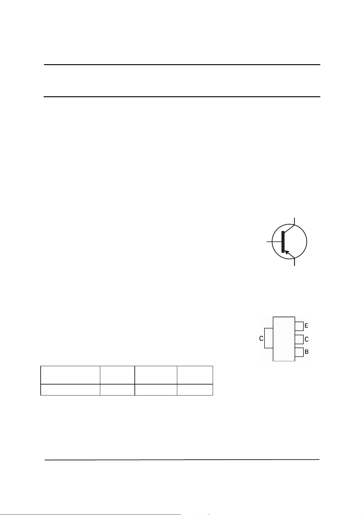
C
B
E
Ordering Information
Device Reel size
(inches)
ZXTP03200BGTA 7 12 1000
Tape width
(mm)
Quantity
per reel
Device Marking
ZXTP03200BG
Issue 1 - August 2008 1
© Diodes Incorporated 2008
Pin out - top view
www.zetex.com
www.diodes.com
ZXTP03200BG
Absolute Maximum Ratings
Parameter Symbol Limit Unit
Collector-Base Voltage
Collector-Emitter Voltage
Emitter-Base Voltage
Continuous Collector Current
(a)
Base Current
Peak Pulse Current
Power Dissipation at TA =25°C
(a)
Linear Derating Factor
Power Dissipation at TA =25°C
(b)
Linear Derating Factor
Power Dissipation at TA =25°C
(c)
Linear Derating Factor
Power Dissipation at TA =25°C
(d)
Linear Derating Factor
Power Dissipation at TC =25°C
(e)
Linear Derating Factor
Operating and Storage Temperature Range
T
V
V
V
j
CBO
CEO
EBO
I
C
I
B
I
CM
P
P
P
P
P
, T
D
D
D
D
D
stg
-220 V
-200 V
-7 V
-2 A
-1 A
-5 A
1.25
10
1.65
13.2
3
24
5.8
46.5
11.9
95.2
-55 to 150
W
mW/°C
W
mW/°C
W
mW/°C
W
mW/°C
W
mW/°C
°C
Thermal Resistance
Parameter Symbol Value Unit
Junction to Ambient
Junction to Ambient
Junction to Ambient
Junction to Ambient
Junction to Lead
NOTES:
(a) For a device surface mounted on 15mm x 15mm x 1.6mm FR4 PCB with high coverage of single sided 1oz copper, in still
air conditions.
(b) Mounted on 25mm x 25mm x 1.6mm FR4 PCB with high coverage of single sided 1oz copper, in still air conditions.
(c) Mounted on 50mm x 50mm x 1.6mm FR4 PCB with high coverage of single sided 2oz copper, in still air conditions.
(d) As (c) above measured at t<5 seconds.
(e) Junction to Lead from Collector Tab.Typical
(e)
(a)
(b)
(c)
(d)
R
R
R
R
R
θJA
θJA
θJA
θJA
θJL
100
76
41.6
21.5
10.5
°C/W
°C/W
°C/W
°C/W
°C/W
Issue 1 - August 2008 2
© Diodes Incorporated 2008
www.zetex.com
www.diodes.com
Thermal Characteristics
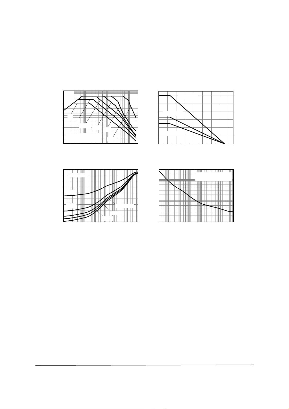
10
V
CE(sat)
Limit
1
DC
1s
100m
Single Pulse. T
Collector Current (A)
C
10m
-I
100m 1 10 100
100ms
10ms
=25°C
amb
See note (c)
-VCE Colle ctor-Emitter Vo l t a g e (V)
Safe Operating Area
1ms
100µs
ZXTP03200BG
3.0
2.5
2.0
See note (b)
1.5
1.0
See note (a)
0.5
0.0
0 20 40 60 80 100 120 140 160
Max Power Dissipation (W)
See note (c)
Temperature (°C)
Derating Curve
40
See note (c)
30
D=0.5
20
D=0.2
10
0
100µ 1m 10m 100m 1 10 100 1k
Thermal Resistance (°C/W)
Pulse Width ( s)
Single Pulse
D=0.05
D=0.1
Transient Thermal Impedance
Single Pulse. T
100
10
1
100µ 1m 10m 100m 1 10 100 1k
Max Power Dissipation (W)
Pulse Width ( s)
See note (c)
Pulse Power Dissipation
amb
=25°C
Issue 1 - August 2008 3
© Diodes Incorporated 2008
www.zetex.com
www.diodes.com
 Loading...