

Diodes ZXTN5551FL User Manual
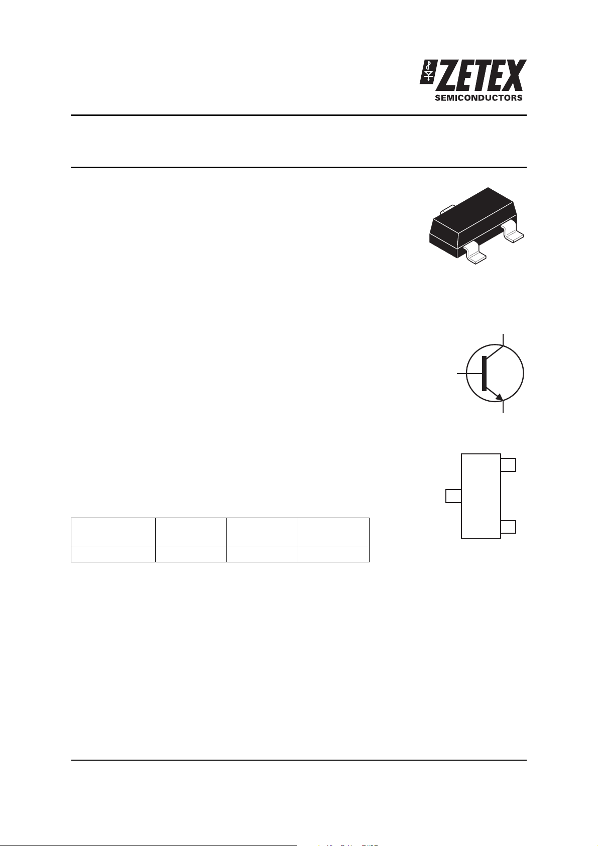
ZXTN5551FL
C
E
B
C
E
B
Pinout - top view
160V, SOT23, NPN High voltage transistor
Summary
BV
BV
I
P
Complementary part number ZXTP5401FL
> 160V
CEO
> 6V
EBO
= 600mA
C(cont)
= 330mW
D
Description
A high voltage NPN transistor in a small outline surface mount package.
Features
•160V rating
• SOT23 package
Applications
• High voltage amplification
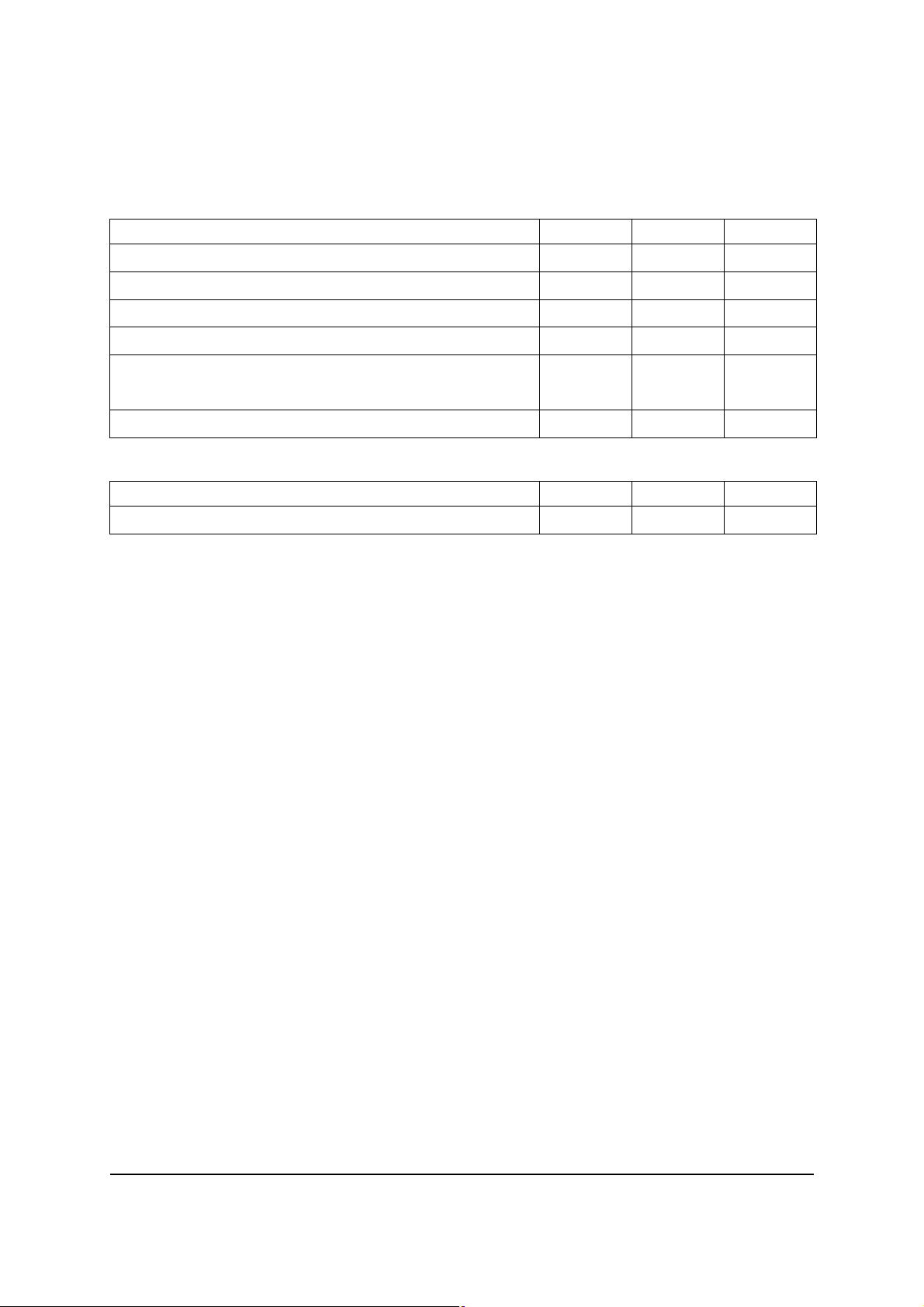
Ordering information
Device Reel size
(inches)
ZXTN5551FLTA 7 8 3000
Tape width
(mm)
Quantity
per reel
Device marking
N51
Issue 1 - August 2007 1 www.zetex.com
© Zetex Semiconductors plc 2007
ZXTN5551FL
Absolute maximum ratings
Parameter Symbol Limit Unit
Collector-base voltage V
Collector-emitter voltage V
Emitter-base voltage V
Continuous collector current
Power dissipation at T
amb
(a)
=25°C
(a)
CBO
CEO
EBO
I
C
P
D
Linear derating factor 2.64 mW/°C
Operating and storage temperature range T
j
, T
stg
Thermal resistance
Parameter Symbol Limit Unit
Junction to ambient
NOTES:
(a) For a device surface mounted on 25mm x 25mm x 1.6mm FR4 PCB with high coverage of single sided 1oz copper, in
still air conditions.
(a)
R
⍜JA
180 V
160 V
6V
600 mA
330 mW
-55 to 150 °C
379 °C/W
Issue 1 - August 2007 2 www.zetex.com
© Zetex Semiconductors plc 2007
ZXTN5551FL
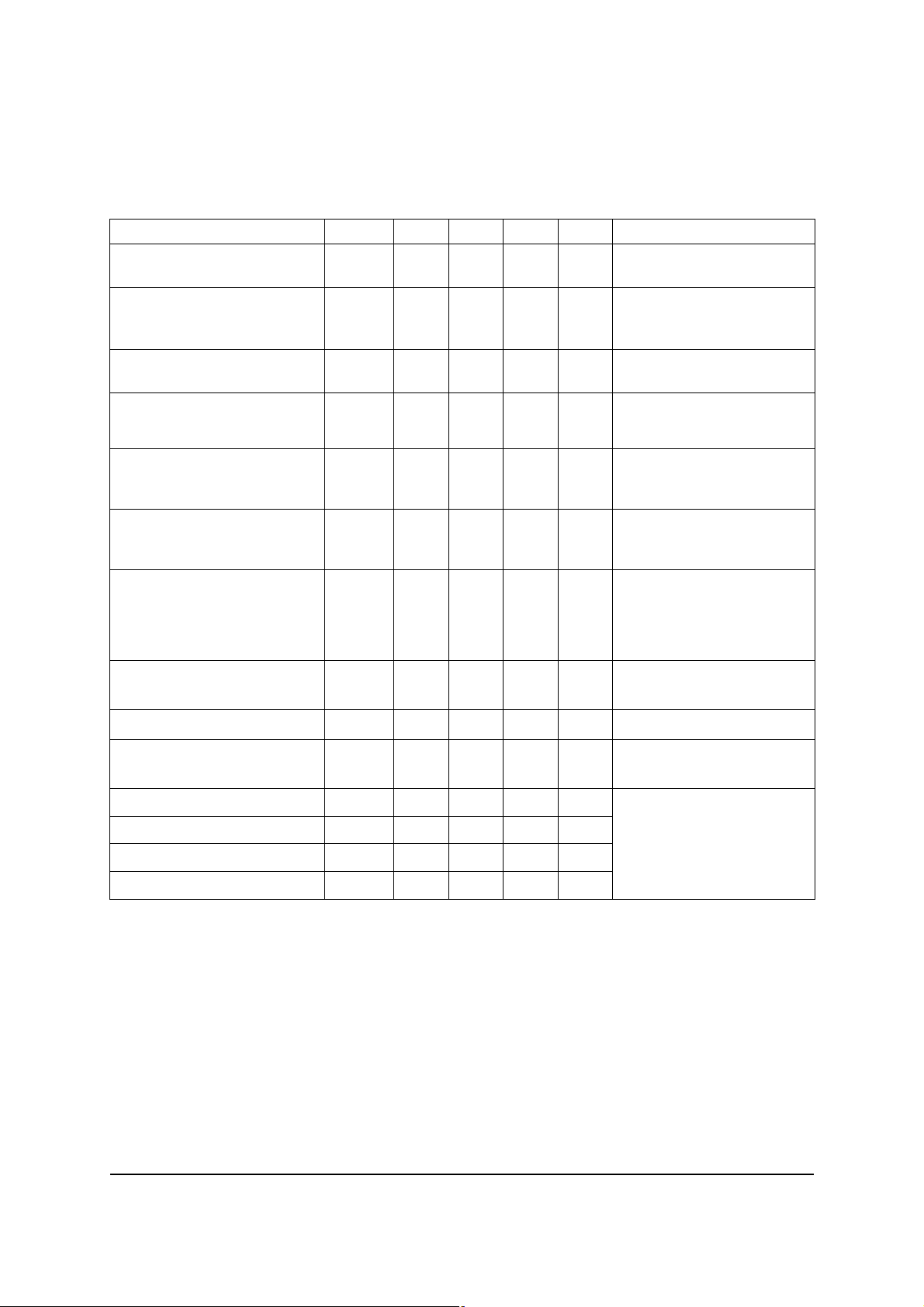
NOTES:
Electrical characteristics (at T
= 25°C unless otherwise stated)
amb
Parameter Symbol Min. Typ. Max. Unit Conditions
Collector-base breakdown
BV
CBO
180 270 V IC = 100A
voltage
Collector-emitter
breakdown voltage (base
BV
CEO
160 200 V
= 1mA
I
C
open)
Emitter-base breakdown
BV
EBO
67.85 VIE = 10A
voltage
Collector cut-off current I
Collector-emitter saturation
voltage
Base-emitter saturation
voltage
Static forward current
transfer ratio
Transition frequency f
Output capacitance C
Small signal h
Delay time t
Rise time t
Storage time t
Fall time t
CBO
V
CE(sat)
V
BE(sat)
h
FE
T
OBO
FE
(d)
(r)
(s)
(f)
<1 50 nA V
50 AV
65 150 V
115 200 V
760 1000 mV
840 1200 mV
80 135
80 145 250
30 65
130 MHz IC = 10mA, VCE = 10V,
6pF
50 260 IC = 10mA, VCE = 10V,
95 ns V
64 ns
1256 ns
140 ns
= 120V
CB
= 120V, T
CB
= 10mA, IB = 1mA
I
C
= 50mA, IB = 5mA
I
C
= 10mA, IB = 1mA
I
C
= 50mA, IB = 5mA
I
C
= 1mA, VCE = 5V
I
C
= 10mA, VCE = 5V
I
C
= 50mA, VCE = 5V
I
C
= 100MHz
f
= 10V, f = 1MHz
V
CB
f=1kHz
I
(†)
= 10V, IC = 10mA, I
CC
= 1mA
B2
(*)
amb
= 100°C
(*)
(*)
(*)
(*)
(*)
(*)
(*)
(*)
B1
=
(*) Measured under pulsed conditions. Pulse width ⱕ300s; duty cycle ⱕ2%.
(†) Periodic sample test only
Issue 1 - August 2007 3 www.zetex.com
© Zetex Semiconductors plc 2007
 Loading...