

Page 1
A
f
Product Line o
HIGH GAIN, LOW V
Features
• High Gain Low Vcesat NPN transistor
• Very Low Rcesat
• High ICM capability
• 1.5A Continuous Current Rating
• Ultra-Small Surface mount Package
• Qualified to AEC-Q101 Standards for High Reliability
• Lead, Halogen and Antimony Free, RoHS Compliant (Note 1)
• “Green” Device (Note 2)
• ESD rating: 400V-MM, 8KV-HBM
Mechanical Data
• Case: DFN1411-3
• Case Material: Molded Plastic, “Green” Molding Compound.
UL Flammability Classification Rating 94V-0
• Moisture Sensitivity: Level 1 per J-STD-020
• Terminals: Finish – NiPdAu over Copper lead frame. Solderable
per MIL-STD-202, Method 208
• Weight: 0.003 grams (approximate)
Applications
• MOSFET and IGBT gate driving
• DC-DC conversion
• Interface between low voltage IC and Load
• LED driving
Diodes Incorporated
CE(SAT)
NPN BIPOLAR TRANSISTOR
ZXTN26020DMF
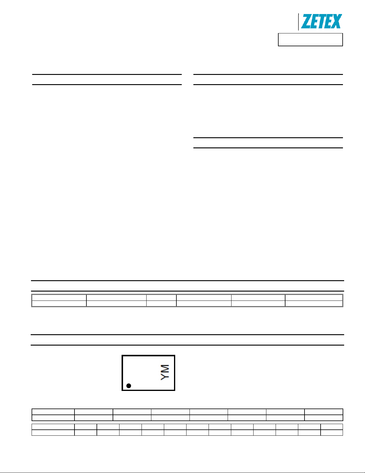
Top view
Device Symbol Bottom view
Pin-out Top view
Ordering Information
Product Status Marking Reel size (inches) Tape width (mm) Quantity per reel
ZXTN26020DMFTA Active Z1 7 8 3000
Notes: 1. No purposefully added lead. Halogen and Antimony Free.
2. Diodes Inc’s “Green” Policy can be found on our website at http://www.diodes.com
Marking Information
Date Code Key
Year 2009 2010 2011 2012 2013 2014 2015
Code W X Y Z A B C
Month Jan Feb Mar Apr May Jun Jul Aug Sep Oct Nov Dec
Code 1 2 3 4 5 6 7 8 9 O N D
ZXTN26020DMF
Documnt Number: DS31953 Rev. 2 - 1
Z1
Z1 = Product Type Marking Code
YM = Date Code Marking
Y = Year (ex: W = 2009)
M = Month (ex: 9 = September)
1 of 6
www.diodes.com
September 2009
© Diodes Incorporated
Page 2
A
f
θ
θ
P, P
OWER
PATIO
P(pk), P
T
RAN
N
T P
OWER
)
T
R
T T
HER
R
T
C
Product Line o
Diodes Incorporated
ZXTN26020DMF
Maximum Ratings
Characteristic Symbol Value Unit
Collector-Base Voltage
Collector-Emitter Voltage
Emitter-Base Voltage
Continuous Collector Current (Note 4)
Peak Pulse Current
Base Current
V
CBO
V
CEO
V
EBO
I
C
I
CM
I
B
20 V
20 V
7 V
1.5 A
4 A
0.5 A
Thermal Characteristics
Characteristic Symbol Value Unit
Power Dissipation (Note 3)
Power Dissipation (Note 4)
Thermal Resistance, Junction to Ambient (Note 3) @ TA = 25°C
Thermal Resistance, Junction to Ambient (Note 3) @ TA = 25°C
Operating and Storage Temperature Range
Notes: 3. Device mounted on FR-4 PCB with 1inch square pads.
4. Device mounted on FR-4 PCB with minimum recommended pad layout
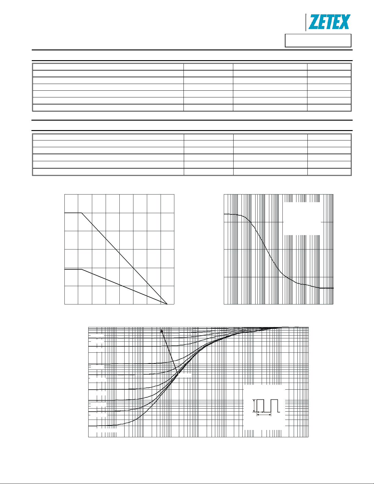
1.2
1.0
Note 3
N (W)
0.8
P
P
R
R
T
J, TSTG
D
D
JA
JA
1,000
(W
100
1 W
380 mW
125
330
-55 to +150
Single Pulse
R (t) = r(t) *
θ
JA
R = 328°C/W
T - T = P * R (t)
JA JA12θ
Duty Cycle, D = t /t
R
JA
θθJA
°C/W
°C/W
°C
SIE
0.6
10
DISSI
0.4
Note 4
D
EAK
1
0.2
0
0 20 40 60 80 100 120 140 160
T , AMBIENT TEMPERATURE ( C)
A
°
Fig. 1 Power Dissipation vs. Ambient Temperature
0.1
0.00001 0.001 0.1 10 1,000
t , PULSE DURATION TIME (s)
1
Fig. 2 Single Pulse Maximum Power Dissipation
1
D = 0.7
E
D = 0.5
AN
D = 0.3
ESIS
0.1
D = 0.1
MAL
D = 0.05
D = 0.02
0.01
D = 0.01
ANSIEN
D = 0.005
r(t),
D = Single Pulse
0.001
0.00001 0.0001 0.001 0.01 0.1 1 10 100 1,000
D = 0.9
t , PULSE DURATION TIME (s)
1
R (t) = r(t) *
θ
JA
R = 328°C/W
JA
P(pk)
t
1
t
2
T - T = P * R (t)
JA JA12θ
Duty Cycle, D = t /t
R
θθJA
Fig. 3 Transi ent Therma l R esponse
ZXTN26020DMF
Documnt Number: DS31953 Rev. 2 - 1
2 of 6
www.diodes.com
September 2009
© Diodes Incorporated
Page 3

A
f
(BR)
(BR)
(BR)
(BR)
)
)
)
r
C
O
CTO
R C
U
R
R
N
T
C
CUR
R
T
G
Product Line o
Diodes Incorporated
ZXTN26020DMF
Electrical Characteristics (at T
= 25°C unless otherwise specified)
A
Characteristic Symbol Min Typ Max Unit Test Condition
Collector-Base Breakdown Voltage
Collector-Emitter Breakdown Voltage (Note 5)
Emitter-Base Breakdown Voltage
Emitter-Collector Breakdown Voltage
V
CBO
V
CEO
V
EBO
V
ECO
Collector Cutoff Current Icbo
Emitter Cutoff Current Ices
Base Cutoff Current Iebo
DC Current Gain (Note 5)
Collector-Emitter Saturation Voltage (Note 5)
Equivalent On-Resistance
Base-Emitter Turn-On Voltage
Base-Emitter Saturation Voltage
Output Capacitance (Note 5)
Input Capacitance (Note 5)
Current Gain-Bandwidth Product
Turn-On Time
Delay Time
Rise Time
Turn-Off Time
Storage Time
Fall Time
Notes: 5. Short duration pulse test used to minimize self-heating effect.
h
FE
V
CE(SAT)
R
CE(SAT
V
BE(ON
V
BE(SAT
C
obo
C
ibo
f
T
t
⎯
on
t
⎯
d
t
⎯
t
⎯
off
t
⎯
s
t
⎯
f
⎯
⎯ ⎯
⎯ ⎯
⎯ ⎯
20
20
7
5
⎯ ⎯
⎯ ⎯
⎯ ⎯
300
290
270
200
⎯
⎯
⎯
⎯
⎯
⎯
—
⎯
⎯ ⎯
⎯ ⎯
⎯ ⎯
⎯ ⎯
1000
⎯
⎯
⎯
⎯
⎯
⎯
⎯
⎯
⎯
⎯
90
⎯
260
60
20
40
225
205
20
V
V
V
V
100
0.5
nA
μA
100 nA
100 nA
⎯
⎯
⎯
⎯
45
70
125
225
225
290
⎯
mV
mV
mV
mV
mV
mV
mΩ
1.2 V
1.1 V
20 pF
150 pF
⎯
⎯
⎯
⎯
⎯
⎯
⎯
MHz
ns
ns
ns
ns
ns
ns
IC = 100μA, IE = 0A
IC = 10mA, IB = 0A
IE = 100μA, IC = 0A
IE = 100μA, IB = 0A
= 20V, IE = 0A
V
CB
V
= 20V, IE = 0, TA = 125°C
CB
V
= 20V, VBE = 0V
CE
V
= 5.6V, IC = 0A
BE
= 2V, IC = 100mA
V
CE
= 2V, IC = 0.5A
V
CE
V
= 2V, IC = 1A
CE
= 2V, IC = 2A
V
CE
IC = 100mA, IB = 1mA
I
= 500mA, IB = 25mA
C
= 1A, IB = 50mA
I
C
I
= 1.5A, IB = 30mA
C
= 2A, IB = 100mA
I
C
I
= 2A, IB = 40mA
C
IC = 1A, IB = 50mA
VCE = 2V, IC = 2A
IC = 2A, IB = 100mA
VCB = 10V, f = 1.0MHz
VEB = 0.5V, f = 1.0MHz
V
= 10V, IC = 50mA,
CE
f = 100MHz
V
= 10V, IC = 1A
CC
= -IB1 = 50mA
I
B2
2.8
2.4
I = 5mA
(A)
2.0
E
1.6
1.2
B
I = 4mA
B
I = 3mA
B
I = 2mA
B
LLE
0.8
C
I,
I = 1mA
B
0.4
1,200
1,100
1,000
AIN
EN
FE
h, D
900
800
700
600
500
400
300
200
T = 150°C
A
T = 125°C
A
T = 85°C
A
T = 25°C
A
T = -55°C
A
100
0
012 345
V , COLLECTOR-EMITTER VOLTAGE (V)
CE
Fig. 4 Typical Collector Current
vs. Collector-Emitter Voltage
0
0.001 0.01 0.1 1 10
I , COLLECTOR CURRENT (A)
Fig. 5 Typical DC Curr ent G ain vs. Co llector Curr ent
C
ZXTN26020DMF
Documnt Number: DS31953 Rev. 2 - 1
3 of 6
www.diodes.com
September 2009
© Diodes Incorporated
Page 4

A
f
C
O
CTO
R
T
TER
T
TER TURN-O
O
T
G
T
TER
TURATIO
N VOLTAG
CAPACITAN
C
G
N
N
T
H PRODU
C
T
H
Product Line o
Diodes Incorporated
ZXTN26020DMF
1
I/I = 20
CB
1.0
E (V)
V = 5V
A
L
CE
0.8
0.1
-EMI
VOLTAGE (V)
T = 125°C
A
T = 150°C
A
T = 25°C
T = -55°C
A
LLE
0.01
SATURATION
CE(SAT)
V,
0.001
0.1 1 10 100 1,000 10,000
Fig. 6 Typical Collector-Emitter Saturation Voltage
I , COLLECTOR CURRENT (mA)
C
vs. Collector Current
1.2
I = 10
/I
E (V)
CB
1.0
0.8
T = -55°C
A
0.6
T = 25°C
A
SA
0.4
T = 150°C
A
T = 125°C
A
T = 85°C
A
0.2
A
T = 85°C
A
N V
T = -55°C
A
0.6
T = 25°C
A
0.4
T = 85°C
A
T = 125°C
0.2
T = 150°C
A
BE(ON)
V , BASE-EMI
0
0.1 1 10 100 1,000 10,000
I , COLLECTOR CURRENT (mA)
Fig. 7 Typical Base-Emitter Turn-On Voltage
A
C
vs. Collector Current
1,000
f = 1MHz
100
E (pF)
C
ibo
C
10
obo
0
0.1 1 10 100 1,000 10,000
BE(SAT)
V , BASE-EMI
I , COLLECTOR CURRENT (mA)
C
Fig. 8 Typical Base-Emitter Saturation Voltage
vs. Collector Current
500
z)
V = 10V
(M
400
CE
1
0 5 10 15 20 25 30 35 40
V , REVERSE VOLTAGE (V)
R
Fig. 9 Typical Capacitance Characteristics
100
V = 20V
CBE
I = 0
C
300
10
200
DWID
-BA
AI
100
T
f,
0
0 5 10 15 20 25 30 35 40 45 50
I , COLLECTOR CURRENT (mA)
C
Fig. 10 Typica l G ain-Bandwidt h Pr oduct vs . C ollector Curr e nt
ZXTN26020DMF
Documnt Number: DS31953 Rev. 2 - 1
4 of 6
www.diodes.com
CBO
I , COLLECTOR CUTOFF CURRENT (nA)
1
-50 -25 0 25 50 75 100 125 150
T , AMBIENT TEMPERATURE (°C)
A
Fig. 11 Collector Cutoff Current vs. Ambient Temperature
September 2009
© Diodes Incorporated
Page 5

A
f
Package Outline Dimensions
A
A1
Suggested Pad Layout
X1
C
Y
G1
Z
X2
G2
Product Line o
Diodes Incorporated
ZXTN26020DMF
DFN1411-3
Dim Min Max Typ
A 0.47 0.53 0.50
A1 0 0.05 0.02
b 0.25 0.35 0.30
D 1.35 1.475 1.40
D2 0.65 0.85 0.75
E 1.05 1.18 1.10
e
⎯ ⎯
L 0.225 0.325 0.275
L1
⎯ ⎯
All Dimensions in mm
Dimensions Value (in mm)
Z 1.38
G1 0.15
X
G2 0.15
X 0.95
X1 0.75
X2 0.40
Y 0.75
C 0.76
0.55
0.20
ZXTN26020DMF
Documnt Number: DS31953 Rev. 2 - 1
5 of 6
www.diodes.com
September 2009
© Diodes Incorporated
Page 6

A
f
Product Line o
IMPORTANT NOTICE
DIODES INCORPORATED MAKES NO WARRANTY OF ANY KIND, EXPRESS OR IMPLIED, WITH REGARDS TO THIS DOCUMENT,
INCLUDING, BUT NOT LIMITED TO, THE IMPLIED WARRANTIES OF MERCHANTABILITY AND FITNESS FOR A PARTICULAR PURPOSE
(AND THEIR EQUIVALENTS UNDER THE LAWS OF ANY JURISDICTION).
Diodes Incorporated and its subsidiaries reserve the right to make modifications, enhancements, improvements, corrections or other changes
without further notice to this document and any product described herein. Diodes Incorporated does not assume any liability arising out of the
application or use of this document or any product described herein; neither does Diodes Incorporated convey any license under its patent or
trademark rights, nor the rights of others. Any Customer or user of this document o r products described herein in such applica tions shall assume
all risks of such use and will agree to hold Diodes Incorporated and all the companies whose products are represented on Diodes Incorporated
website, harmless against all damages.
Diodes Incorporated does not warrant or accept any liability whatsoever in respect of any products purchased through unauthorized sales channel.
Should Customers purchase or use Diodes Incorporated products for any unintended or unauthorize d application, Customers shall indemnify and
hold Diodes Incorporated and its representatives harmless against all claims, damages, expenses, and attorney fees arising out of, directly or
indirectly, any claim of personal injury or death associated with such unintended or unauthorized application.
Products described herein may be covered by one or more United States, international or foreign patents pending. Product names and markings
noted herein may also be covered by one or more United States, international or foreign trademarks.
LIFE SUPPORT
Diodes Incorporated products are specifically not authorized for use as critical components in life support devices or systems without the express
written approval of the Chief Executive Officer of Diodes Incorporated. As used herein:
A. Life support devices or systems are devices or systems which:
1. are intended to implant into the body, or
2. support or sustain life and whose failure to perform when properly used in accordance with instructions for use provided in the
labeling can be reasonably expected to result in significant injury to the user.
B. A critical component is any component in a life support device or system whose failure to perform can be reasonably expected to cause
the failure of the life support device or to affect its safety or effectiveness.
Customers represent that they have all necessary expertise in the safety and regulatory ramifications of their life support devices or systems, and
acknowledge and agree that they are solely responsible for all legal, regulatory and safety-related requirements concerning their products and any
use of Diodes Incorporated products in such safety-critical, life support devices or systems, notwithstanding any devices- or systems-related
information or support that may be provided by Diodes Incorporated. Further, Customers must fully indemnify Diodes Incorporated and its
representatives against any damages arising out of the use of Diodes Incorporated products in such safety-critical, life support devices or systems.
Copyright © 2009, Diodes Incorporated
www.diodes.com
Diodes Incorporated
ZXTN26020DMF
ZXTN26020DMF
Documnt Number: DS31953 Rev. 2 - 1
6 of 6
www.diodes.com
September 2009
© Diodes Incorporated
 Loading...