

Page 1
A
f
Product Line o
40V NPN MEDIUM POWER PLANAR TRANSISTOR IN SOT23
Features and Benefits
• BV
• I
• Low Saturation Voltage V
• R
• h
• High h
• 1.25W power dissipation
• 130V forward blocking voltage
• 6V reverse blocking voltage
• Complementary part number ZXTP25040DFH
• “Lead-Free”, RoHS Compliant (Note 1)
• Halogen and Antimony Free. “Green” Device (Note 2)
• Qualified to AEC-Q101 Standards for High Reliability
> 40V
CEO
= 4A Continuous Collector Current
C
= 35mΩ
CE(sat)
characterised up to 10A
FE
min 300 @ 1A
FE
CE(sat)
SOT23
< 55mV @ 1A
Mechanical Data
• Case: SOT23
• Case material: Molded Plastic. “Green” Molding Compound
(Note 2) UL Flammability Classification Rating 94V-0
• Moisture Sensitivity: Level 1 per J-STD-020
• Terminals: Matte Tin Finish; Solderable per MIL-STD-202,
Method 208
• Weight: 0.008 grams (Approximate)
Applications
• MOSFET gate drivers
• Power switches
• Motor control
• DC fans
• DC-DC converters
Diodes Incorporated
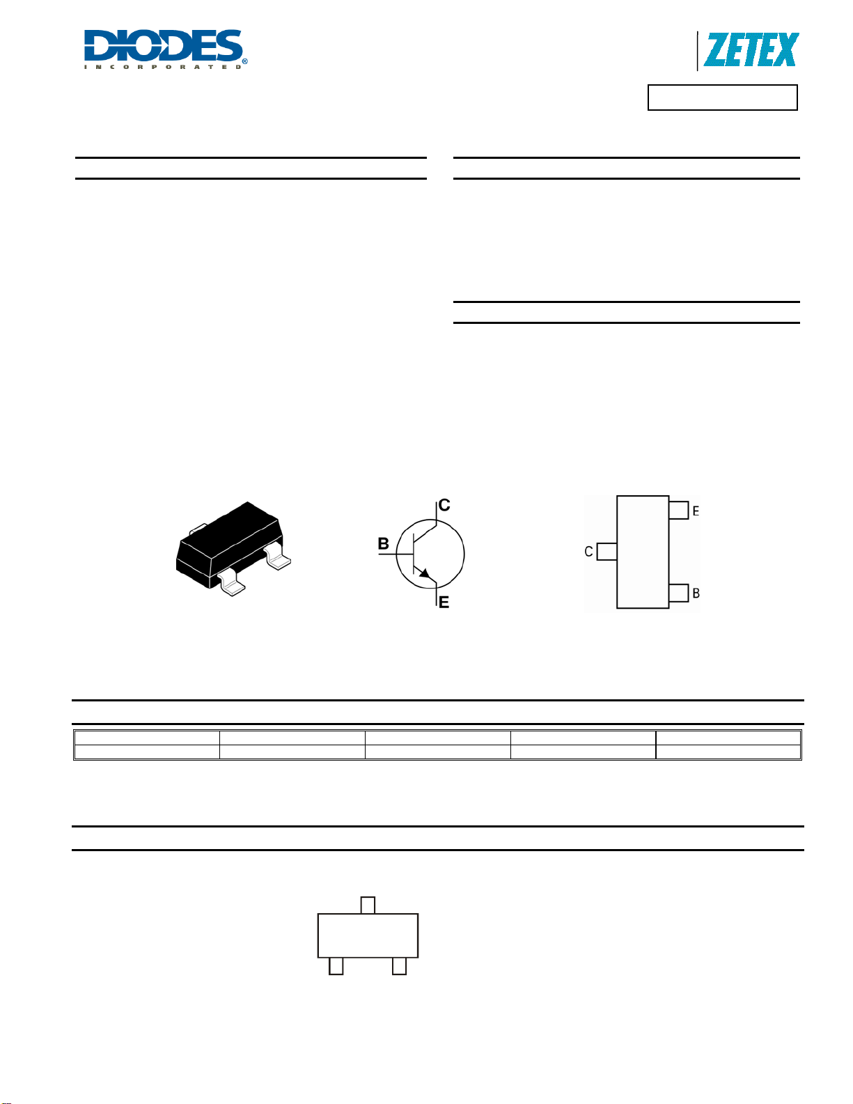
ZXTN25040DFH
Top View
Device Symbol
Top View
Pin Configuration
Ordering Information (Note 3)
Product Marking Reel size (inches) Tape width (mm) Quantity per reel
ZXTN25040DFHTA 1A4 7 8 3,000
Notes: 1. No purposefully added lead.
2. Diodes Inc‘s “Green” Policy can be found on our website at https://www.diodes.com/
3. Devices with lot number starting from PID0155145 (March 2010) are “Green” products.
Marking Information
ZXTN25040DFH
Document number: DS33697 Rev. 2 - 2
1A4
www.diodes.com
1A4 = Product Type Marking Code
1 of 7
January 2012
© Diodes Incorporated
Page 2
A
f
Product Line o
Diodes Incorporated
ZXTN25040DFH
Maximum Ratings @T
= 25°C unless otherwise specified
A
Characteristic Symbol Value Unit
Collector-Base Voltage
Collector-Emitter Voltage (Forward Blocking)
Collector-Emitter Voltage
Emitter-Collector Voltage (Reverse Blocking)
Emitter-Base Voltage
Continuous Collector Current (Note 6)
Peak Pulse Current
Base Current
V
CBO
V
CEX
V
CEO
V
ECO
V
EBO
I
C
I
CM
I
B
130 V
130 V
40 V
6 V
7 V
4 A
10 A
1 A
Thermal Characteristics @T
= 25°C unless otherwise specified
A
Characteristic Symbol Value Unit
0.73
5.84
1.05
8.4
1.25
9.6
1.81
14.5
171
W
mW/°C
°C/W
Power Dissipation
Linear Derating Factor
Thermal Resistance, Junction to Ambient
(Note 4)
(Note 5)
(Note 6)
P
D
-
(Note 7)
(Note 4)
(Note 5) 119
(Note 6) 100
R
θJA
(Note 7) 69
Thermal Resistance, Junction to Lead (Note 8)
Operating and Storage Temperature Range
Notes: 4. For a device surface mounted on 15mm X 15mm X 1.6mm FR4 PCB with high coverage of single sided 1 oz copper, in still air conditions; the device is
measured when operating in a steady-state condition.
5. For a device surface mounted on 25mm X 25mm X 1.6mm FR4 PCB with high coverage of single sided 2 oz copper, in still air conditions; the device is
measured when operating in a steady-state condition.
6. For a device surface mounted on 50mm X 50mm X 1.6mm FR4 PCB with high coverage of single sided 2 oz copper, in still air conditions; the device is
measured when operating in a steady-state condition.
7. As note 6 above, measured at t < 5 seconds
8. Thermal resistance from junction to solder-point (at the end of the collector lead).
R
T
J, TSTG
θJL
74.95
-55 to +150
°C/W
°C
ZXTN25040DFH
Document number: DS33697 Rev. 2 - 2
2 of 7
www.diodes.com
January 2012
© Diodes Incorporated
Page 3
A
f
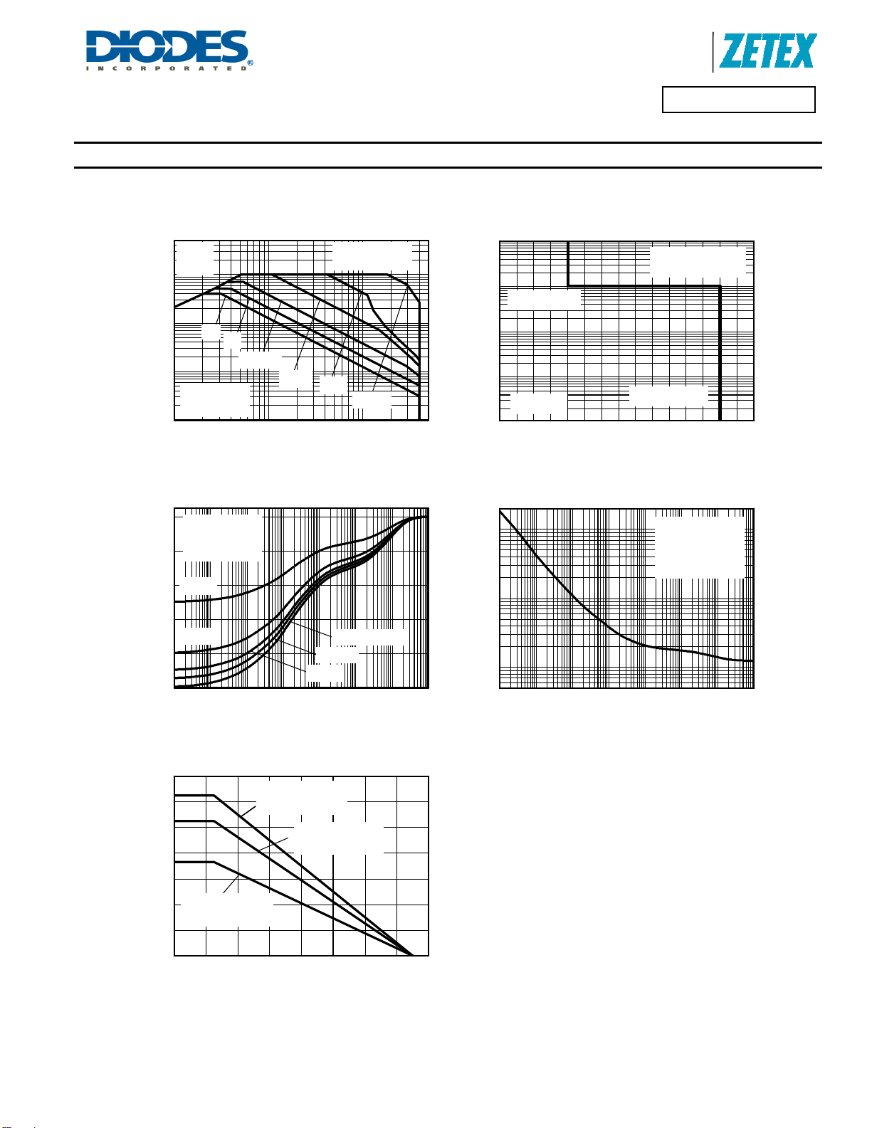
Typical Thermal Characteristics
Product Line o
Diodes Incorporated
ZXTN25040DFH
V
CE(sat)
Limited
10
1
DC
1s
100m
Single Pulse
Collector Curr ent (A)
I
T
C
10m
amb
100m 1 10
100ms
10ms
=25°C
50mmX50mm FR4
2oz Cu
1ms
100µs
VCE Collector-Emitter Voltage (V)
Safe Operating Area
100
T
=25°C
amb
50mm X 50mm FR4
80
2oz Cu
60
D=0.5
40
D=0.2
20
0
100µ 1m 10m 100m 1 10 100 1k
Thermal Resistance (°C/W)
Puls e Width (s )
Single Pulse
D=0.05
D=0.1
1m
Failu r e may occ ur
in this region
100µ
BV
=40V
(BR)CEO
10µ
1µ
BV
=130V
T
Collector Current (A)
C
I
=25°C
amb
0 20 40 60 80 100 120 140
(BR)CEX
VCE Collector-Emitter Voltage (V)
Safe Operating Area
100
10
1
Maximum Power (W)
100µ 1m 10m 100m 1 10 100 1k
Puls e Width (s)
Single Pulse
T
=25°C
amb
50mmX50 mm FR4
2oz Cu
Transient Thermal Impedance
Pulse Power Dissipation
1.4
1.2
1.0
0.8
50mmX50mm F R4
2oz Cu
25mmX 25mm FR4
2oz Cu
0.6
15mmX 15mm FR4
0.4
1oz Cu
0.2
0.0
0 20 40 60 80 100 120 140 160
Max Power Dissipati on (W)
Temperature (°C)
Derating Curve
ZXTN25040DFH
Document number: DS33697 Rev. 2 - 2
3 of 7
www.diodes.com
January 2012
© Diodes Incorporated
Page 4

A
f
)
)
r
Product Line o
Diodes Incorporated
ZXTN25040DFH
Electrical Characteristics @T
= 25°C unless otherwise specified
A
Characteristic Symbol Min Typ Max Unit Test Condition
OFF CHARACTERISTICS
Collector-Base Breakdown Voltage
Collector-emitter breakdown voltage
(forward blocking)
Collector-Emitter Breakdown Voltage
(base open) (Note 9)
Emitter-Base Breakdown Voltage
Emitter-collector breakdown voltage
(reverse blocking)
Emitter-collector breakdown voltage
(base open)
Collector-base Cut-off Current
Collector-emitter Cut-off Current
Emitter-base Cut-off Current
BV
BV
BV
BV
BV
BV
I
CBO
I
CEX
I
EBO
CBO
CEX
CEO
EBO
ECX
ECO
ON CHARACTERISTICS (Note 9)
Static Forward Current Transfer Ratio
Collector-Emitter Saturation Voltage
Base-Emitter Saturation Voltage
Base-Emitter On Voltage
V
CE(sat)
V
BE(sat
V
BE(on
h
FE
SMALL SIGNAL CHARACTERISTICS (Note 9)
Transition Frequency
Collector Output Capacitance
Delay time
Rise time
Storage time
Fall time
Notes: 9. Measured under pulsed conditions. Pulse width ≤ 300µs. Duty cycle ≤ 2%
f
T
C
obo
t
d
t
t
s
t
f
130 170 - V
130 170 - V
40 63 - V
7 8.3 - V
6 7.4 - V
6 7.4 - V
-
<1
50
-
20
- - 100 nA
- <1 50 nA
300
300
30
-
-
450
450
60
10
45
120
135
140
900
-
-
-
55
210
210
190
- 960 1050 mV
- 840 950 mV
- 190 - MHz
- 11.7 20 pF
- 64 - ns
- 108 -
- 428 -
- 130 -
IC = 100µA
= 100µA; RBE < 1kΩ or
I
C
-1V < V
IC = 10mA
IE = 100µA
= 100µA; RBC < 1kΩ or
I
E
-0.25V < V
I
= 100µA;
E
V
nA
µA
CB
V
CB
V
CE
-1V < V
VEB = 5.6V
I
= 10mA, V
C
= 1A, V
I
C
I
= 4A, V
C
= 10A, V
I
C
I
= 1A, IB = 100mA
C
I
= 1A, IB = 10mA
mV
C
= 2A, IB = 40mA
I
C
I
= 4A, IB = 400mA
C
IC = 4A, IB = 400mA
IC = 4A, V
= 50mA, VCE = 10V,
I
C
f = 100MHz
VCB = 10V, f = 1MHz
V
ns
ns
ns
CC
= 1A,
I
C
I
= IB2 = 10mA
B1
< 0.25V
BE
< 0.25V
BC
= 100V
= 100V, TA = 100°C
= 100V; RBE < 1kΩ or
< 0.25V
BE
= 2V
CE
= 2V
CE
= 2V
CE
= 2V
CE
= 2V
CE
= 10V,
ZXTN25040DFH
Document number: DS33697 Rev. 2 - 2
4 of 7
www.diodes.com
January 2012
© Diodes Incorporated
Page 5

A
f
Typical Electrical Characteristics
Product Line o
Diodes Incorporated
ZXTN25040DFH
1
Tamb=25°C
IC/IB=100
100m
(V)
10m
CE(SAT)
V
1m
1m 10m 100m 1 10
IC/IB=20
IC/IB=10
IC Colle cto r C urrent (A)
V
1.6
1.4
1.2
1.0
0.8
0.6
0.4
Normalised Gain
0.2
0.0
1m 10m 100m 1 10
150°C
100°C
25°C
-55°C
CE(SAT)
v I
C
VCE=2V
IC Collector Curre nt (A)
hFE v I
C
IC/IB=50
825
750
675
600
525
450
375
300
225
150
75
0
0.7
IC/IB=10
0.6
0.5
0.4
(V)
0.3
CE(SAT)
0.2
V
0.1
0.0
10m 100m 1 10
150°C
100°C
25°C
-55°C
IC Colle cto r C urrent (A)
V
1.2
IC/IB=10
FE
1.0
0.8
(V)
0.6
BE(SAT)
V
0.4
1m 10m 100m 1 10
)
Typical Gain (h
CE(SAT)
25°C
v I
-55°C
C
100°C
150°C
IC Colle cto r C urrent (A)
V
BE(SAT)
v I
C
1.0
0.8
VCE=2V
25°C
-55°C
(V)
0.6
BE(ON)
V
0.4
0.2
1m 10m 100m 1 10
100°C
150°C
IC Colle cto r C urrent (A)
V
ZXTN25040DFH
Document number: DS33697 Rev. 2 - 2
BE(ON)
v I
C
5 of 7
www.diodes.com
January 2012
© Diodes Incorporated
Page 6

A
f
Package Outline Dimensions
b
3leads
Product Line o
Diodes Incorporated
E
e
e1
ZXTN25040DFH
L1
E1
A
L
A1
c
D
Dim. Millimeters Inches Dim. Millimeters Inches
Min. Max. Min. Max. Min. Max. Min. Max.
A - 1.12 - 0.044 e1 1.90 NOM 0.075 NOM
A1 0.01 0.10 0.0004 0.004 E 2.10 2.64 0.083 0.104
b 0.30 0.50 0.012 0.020 E1 1.20 1.40 0.047 0.055
c 0.085 0.20 0.003 0.008 L 0.25 0.60 0.0098 0.0236
D 2.80 3.04 0.110 0.120 L1 0.45 0.62 0.018 0.024
e 0.95 NOM 0.037 NOM - - - - -
Note: Controlling dimensions are in millimeters. Approximate dimensions are provided in inches
Suggested Pad Layout
0.95
0.037
2.0
0.079
0.9
0.035
0.8
0.031
ZXTN25040DFH
Document number: DS33697 Rev. 2 - 2
6 of 7
www.diodes.com
mm
inches
January 2012
© Diodes Incorporated
Page 7

A
f
Product Line o
IMPORTANT NOTICE
DIODES INCORPORATED MAKES NO WARRANTY OF ANY KIND, EXPRESS OR IMPLIED, WITH REGARDS TO THIS DOCUMENT,
INCLUDING, BUT NOT LIMITED TO, THE IMPLIED WARRANTIES OF MERCHANTABILITY AND FITNESS FOR A PARTICULAR PURPOSE
(AND THEIR EQUIVALENTS UNDER THE LAWS OF ANY JURISDICTION).
Diodes Incorporated and its subsidiaries reserve the right to make modifications, enhancements, improvements, corrections or other changes
without further notice to this document and any product described herein. Diodes Incorporated does not assume any liability arising out of the
application or use of this document or any product described herein; neither does Diodes Incorporated convey any license under its patent or
trademark rights, nor the rights of others. Any Customer or user of this document o r products described herein in such applica tions shall assume
all risks of such use and will agree to hold Diodes Incorporated and all the companies whose products are represented on Diodes Incorporated
website, harmless against all damages.
Diodes Incorporated does not warrant or accept any liability whatsoever in respect of any products purchased through unauthorized sales channel.
Should Customers purchase or use Diodes Incorporated products for any unintended or unauthorize d application, Customers shall indemnify and
hold Diodes Incorporated and its representatives harmless against all claims, damages, expenses, and attorney fees arising out of, directly or
indirectly, any claim of personal injury or death associated with such unintended or unauthorized application.
Products described herein may be covered by one or more United States, international or foreign patents pending. Product names and markings
noted herein may also be covered by one or more United States, international or foreign trademarks.
LIFE SUPPORT
Diodes Incorporated products are specifically not authorized for use as critical components in life support devices or systems without the express
written approval of the Chief Executive Officer of Diodes Incorporated. As used herein:
A. Life support devices or systems are devices or systems which:
1. are intended to implant into the body, or
2. support or sustain life and whose failure to perform when properly used in accordance with instructions for use provided in the
labeling can be reasonably expected to result in significant injury to the user.
B. A critical component is any component in a life support device or system whose failure to perform can be reasonably expected to cause the
failure of the life support device or to affect its safety or effectiveness.
Customers represent that they have all necessary expertise in the safety and regulatory ramifications of their life support devices or systems, and
acknowledge and agree that they are solely responsible for all legal, regulatory and safety-related requirements concerning their products and any
use of Diodes Incorporated products in such safety-critical, life support devices or systems, notwithstanding any devices- or systems-related
information or support that may be provided by Diodes Incorporated. Further, Customers must fully indemnify Diodes Incorporated and its
representatives against any damages arising out of the use of Diodes Incorporated products in such safety-critical, life support devices or systems.
Copyright © 2012, Diodes Incorporated
www.diodes.com
Diodes Incorporated
ZXTN25040DFH
ZXTN25040DFH
Document number: DS33697 Rev. 2 - 2
7 of 7
www.diodes.com
January 2012
© Diodes Incorporated
 Loading...