

Page 1
ZXTN23015CFH
15V, SOT23, NPN medium power transistor
Summary
V
(BR)CEX
I
C(CONT)
R
CE(SAT)
V
CE(SAT)
P
D
Complementary part number : ZXTP23015CFH
> 60V, V
= 6A
= 19m⍀ typical
< 30mV @ 1A
= 1.25W
(BR)CEO
> 15V
Description
Advanced process capability and package design have been used to
maximize the power handling and performance of this small outline
transistor. The compact size and ratings of this device make it ideally
suited to applications where space is at a premium.
Features
• Higher power dissipation SOT23 package
• High peak current
• Low saturation voltage
• 60V forward blocking voltage
Applications
•DC - DC converters
• MOSFET and IGBT gate driving
• Motor drive
• Relay, lamp, and solenoid drive
Ordering information
Device Reel size
(inches)
ZXTN23015CFHTA 7 8mm 3000
Tape
width
Quantity per REEL
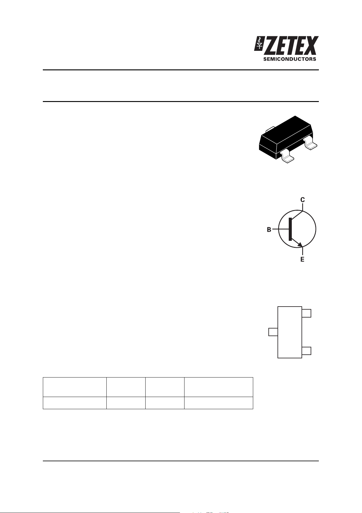
C
Pinout - top view
E
B
Device marking
327
Issue 1 - February 2006 1 www.zetex.com
© Zetex Semiconductors plc 2006
Page 2
ZXTN23015CFH
Absolute maximum ratings
Parameter Symbol Limit Unit
Collector-base voltage V
Collector-emitter voltage V
(BR)CEX
Collector-emitter voltage V
Emitter-base voltage V
Peak pulse current I
Continuous collector current
(c)
Base current I
Power dissipation @ T
Linear derating factor
Power dissipation @ T
Linear derating factor
Power dissipation @ T
Linear derating factor
Power dissipation @ T
Linear derating factor
A
(a)
A
(b)
A
(c)
A
(d)
=25oC
=25oC
=25oC
=25oC
(a)
(b)
(c)
(d)
CBO
CEO
EBO
CM
I
C
B
P
D
P
D
P
D
P
D
60 V
60 V
15 V
7.0 V
12 A
6A
1.2 A
0.73
5.84
1.05
8.4
1.25
9.6
1.81
14.5
W
mW/
W
mW/
W
mW/
W
mW/
o
C
o
C
o
C
o
C
Operating and storage temperature T
j:Tstg
-55 to +150
o
C
Thermal resistance
Parameter Symbol Value Unit
Junction to ambient
Junction to ambient
Junction to ambient
Junction to ambient
NOTES:
(a) For a device surface mounted on 15mm x 15mm x 1.6mm FR4 PCB with high coverage of single sided 1oz copper, in
still air conditions.
(b) Mounted on 25mm x 25mm x 1.6mm FR4 PCB with a high coverage of single sided 2 oz copper in still air conditions.
(c) Mounted on 50mm x 50mm x 1.6mm FR4 PCB with a high coverage of single sided 2 oz copper in still air conditions.
(d) As (c) above measured at t<5secs.
(a)
(b)
(c)
(d)
R⍜
R⍜
R⍜
R⍜
JA
JA
JA
JA
171
119
100
69
Issue 1 - February 2006 2 www.zetex.com
© Zetex Semiconductors plc 2006
o
C/W
o
C/W
o
C/W
o
C/W
Page 3

Characteristics
ZXTN23015CFH
Issue 1 - February 2006 3 www.zetex.com
© Zetex Semiconductors plc 2006
Page 4

ZXTN23015CFH
Electrical characteristics (at T
= 25°C unless otherwise stated)
AMB
Parameter Symbol Min. Typ. Max. Unit Conditions
Collector-base breakdown
V
(BR)CBO
60 85 V IC=100A
voltage
Collector-emitter breakdown
voltage
Collector-emitter breakdown
voltage
Emitter-base breakdown voltage V
Collector-emitter cut-off current I
Collector-base cut-off current I
Emitter-base cut-off current I
Static forward current transfer
ratio
Collector-emitter saturation
voltage
Base-emitter saturation voltage V
Base-emitter turn-on voltage V
Transition frequency f
V
(BR)CEX
V
(BR)CEO
(BR)EBO
CEX
CBO
EBO
H
FE
V
CE(sat)
BE(sat)
BE(on)
T
60 85 V IC =100A,
R
< 1k⍀ OR
BE
15 23 V
-1V < V
I
C
BE
=10mA
7.0 8.3 V IE=100A
-100nAV
= 48V,
CE
< 1k⍀ OR
R
BE
-1V < V
BE
<1 20 nA VCB=48V
<1 10 nA VEB=6V
160 300
200 350 560
190 330
150 280
715mV
22 30 mV
70 90 mV
130 180 mV
0.83 0.93 V
0.89 0.98 V
0.81 0.91 V
=10mA, VCE=2V
I
C
=500mA, VCE=2V
I
C
=3A, VCE=2V
I
C
=6A, VCE=2V
I
C
=0.1A, IB=5mA
I
C
=1A, IB=100mA
I
C
=3A, IB=60mA
I
C
=6A, IB=120mA
I
C
=3A, IB=60mA
I
C
=6A, IB=120mA
I
C
=6A, VCE=2V
I
C
235 MHz Ic=500mA, VCE=2V,
f=50MHz
Output capacitance C
Delay time t
Rise time t
Storage time t
Fall time t
obo
(d)
(r)
(stg)
(f)
56 pF VCB=10V, f=1MHz
15 ns VCC=5V, IC=3A,
38.5 ns
I
B1=IB2
=150mA
213 ns
19.7 ns
< 0.25V
(*)
< 0.25V
(*)
(*)
(*)
(*)
(*)
(*)
(*)
(*)
(*)
(*)
(*)
NOTES:
(*) Measured under pulsed conditions. Pulse width = 300
S. Duty cycle ⱕ2%.
Issue 1 - February 2006 4 www.zetex.com
© Zetex Semiconductors plc 2006
Page 5

Typical characteristics
ZXTN23015CFH
Issue 1 - February 2006 5 www.zetex.com
© Zetex Semiconductors plc 2006
Page 6

Package outline - SOT23
L
ZXTN23015CFH
H
N
D
G
3 leads
M
B
A
C
K
F
Dim. Millimeters Inches Dim. Millimeters Inches
Min. Max. Min. Max. Min. Max. Max. Max.
A 2.67 3.05 0.105 0.120 H 0.33 0.51 0.013 0.020
B 1.20 1.40 0.047 0.055 K 0.01 0.10 0.0004 0.004
C - 1.10 - 0.043 L 2.10 2.50 0.083 0.0985
D 0.37 0.53 0.015 0.021 M 0.45 0.64 0.018 0.025
F 0.085 0.15 0.0034 0.0059 N 0.95 NOM 0.0375 NOM
G 1.90 NOM 0.075 NOM - - - - -
Note: Controlling dimensions are in millimeters. Approximate dimensions are provided in inches
Europe
Zetex GmbH
Streitfeldstraße 19
D-81673 München
Germany
Telefon: (49) 89 45 49 49 0
Fax: (49) 89 45 49 49 49
europe.sales@zetex.com
For international sales offices visit www.zetex.com/offices
Zetex products are distributed worldwide. For details, see www.zetex.com/salesnetwork
This publication is issued to provide outline information only which (unless agreed by the company in writing) may not be used, applied or
reproduced for any purpose or form part of any order or contact or be regarded as a representation relating to the products or services concerned.
The company reserves the right to alter without notice the specification, design, price or conditions of supply of any product or service.
Americas
Zetex Inc
700 Veterans Memorial Highway
Hauppauge, NY 11788
USA
Telephone: (1) 631 360 2222
Fax: (1) 631 360 8222
usa.sales@zetex.com
Asia Pacific
Zetex (Asia Ltd)
3701-04 Metroplaza Tower 1
Hing Fong Road, Kwai Fong
Hong Kong
Telephone: (852) 26100 611
Fax: (852) 24250 494
asia.sales@zetex.com
Corporate Headquarters
Zetex Semiconductors plc
Zetex Technology Park, Chadderton
Oldham, OL9 9LL
United Kingdom
Telephone: (44) 161 622 4444
Fax: (44) 161 622 4446
hq@zetex.com
Issue 1 - February 2006 6 www.zetex.com
© Zetex Semiconductors plc 2006
 Loading...