

Page 1
A
f
45V NPN MEDIUM POWER PLANAR TRANSISTOR IN SOT23F
Features and Benefits
• BV
• I
• Low Saturation Voltage V
• R
• h
• High h
• 1.5W power dissipation
• Complementary part number ZXTP07040DFF
• Totally Lead-Free & Fully RoHS compliant (Note 1)
• Halogen and Antimony Free. “Green” Device (Note 2)
• Qualified to AEC-Q101 Standards for High Reliability
> 45V
CEO
= 4A Continuous Collector Current
C
= 50mΩ
CE(sat)
characterised up to 4A
FE
min 400 @ 1A
FE
< 80mV @ 1A
CE(sat)
Description
This low voltage NPN transistor has been designed for applications
requiring high gain and very low saturation voltage. The SOT23F
package is pin compatible with the industry standard SOT23 footprint
but offers lower profile and higher dissipation for applications where
power density is of utmost importance.
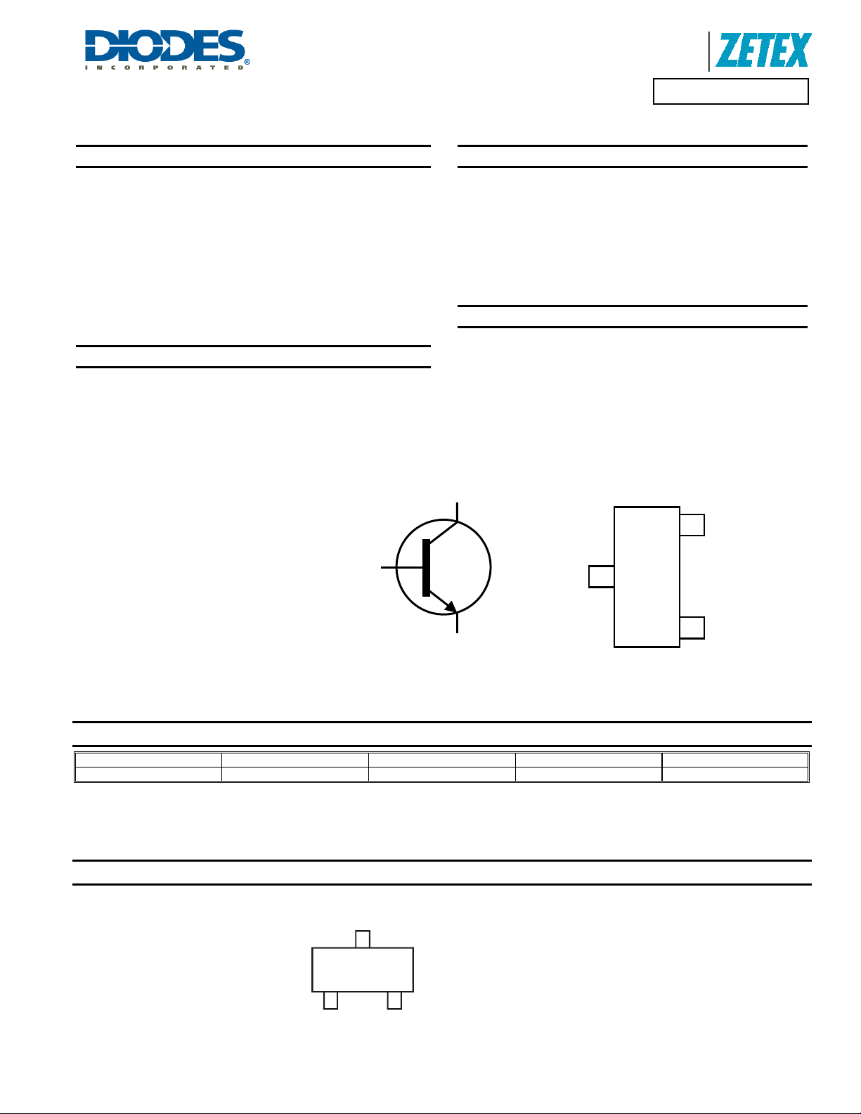
SOT23F
B
Top View
Device symbol
Product Line o
Diodes Incorporated
ZXTN07045EFF
Mechanical Data
• Case: SOT23F
• Case material: Molded Plastic. “Green” Molding Compound
(Note 2) UL Flammability Classification Rating 94V-0
• Moisture Sensitivity: Level 1 per J-STD-020
• Terminals: Matte Tin Finish; Solderable per MIL-STD-202,
Method 208
• Weight: 0.008 grams (Approximate)
Applications
• Boost converters
• MOSFET and IGBT gate drivers
• Lamp and relay driver
• Motor drive
• Siren driver
C
E
C
E
Top View
Pin Configuration
B
Ordering Information (Note 3)
Product Marking Reel size (inches) Tape width (mm) Quantity per reel
ZXTN07045EFFTA 1D4 7 8 3,000
Notes: 1. No purposely added lead. Fully EU Directive 2002/95/EC (RoHS) & 2011/65/EU (RoHS 2) compliant.
3. For packaging details, go to our website at http://www.diodes.com.
2. Halogen and Antimony free "Green” products are defined as those which contain <900ppm bromine, <900ppm chlorine (<1500ppm total Br + Cl) and
<1000ppm antimony compounds.
Marking Information
ZXTN07045EFF
Document number: DS33674 Rev. 4 - 2
1D4
1D4 = Product Type Marking Code
1 of 7
www.diodes.com
February 2012
© Diodes Incorporated
Page 2
A
f
Product Line o
Diodes Incorporated
ZXTN07045EFF
Maximum Ratings @T
= 25°C unless otherwise specified
A
Characteristic Symbol Value Unit
Collector-Base Voltage
Collector-Emitter Voltage
Emitter-Collector Voltage (Reverse Blocking)
Emitter-Base Voltage
Continuous Collector Current (Note 6)
Peak Pulse Current
Base Current
V
CBO
V
CEO
V
ECO
V
EBO
I
C
I
CM
I
B
45 V
45 V
6 V
7 V
4 A
6 A
1 A
Thermal Characteristics @T
= 25°C unless otherwise specified
A
Characteristic Symbol Value Unit
0.84
6.72
1.34
10.72
1.50
12.0
2.0
16.0
149
W
mW/°C
°C/W
Power Dissipation
Linear Derating Factor
Thermal Resistance, Junction to Ambient
(Note 4)
(Note 5)
(Note 6)
P
D
-
(Note 7)
(Note 4)
(Note 5) 93
(Note 6) 83
R
θJA
(Note 7) 60
Thermal Resistance, Junction to Lead (Note 8)
Operating and Storage Temperature Range
Notes: 4. For a device surface mounted on 15mm X 15mm X 1.6mm FR4 PCB with high coverage of single sided 1 oz copper, in still air conditions; the device is
measured when operating in a steady-state condition.
5. For a device surface mounted on 25mm X 25mm X 1.6mm FR4 PCB with high coverage of single sided 2 oz copper, in still air conditions; the device is
measured when operating in a steady-state condition.
6. For a device surface mounted on 50mm X 50mm X 1.6mm FR4 PCB with high coverage of single sided 2 oz copper, in still air conditions; the device is
measured when operating in a steady-state condition.
7. As note 6 above, measured at t < 5 seconds
8. Thermal resistance from junction to solder-point (at the end of the collector lead).
R
T
J, TSTG
θJL
43.77
-55 to +150
°C/W
°C
ZXTN07045EFF
Document number: DS33674 Rev. 4 - 2
2 of 7
www.diodes.com
February 2012
© Diodes Incorporated
Page 3
A
f
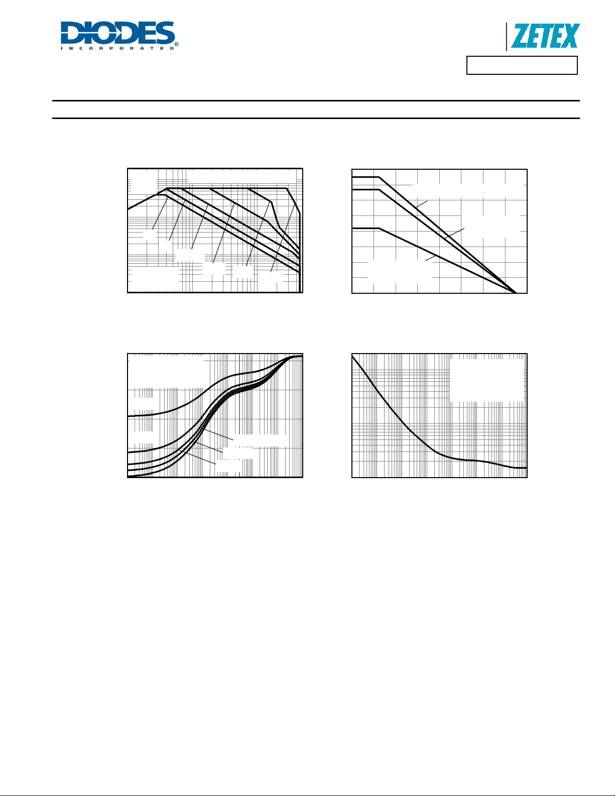
Typical Thermal Characteristics
Product Line o
Diodes Incorporated
ZXTN07045EFF
V
10
CE(sat)
Limited
1
DC
100m
Collector Current (A)
C
I
10m
100m 1 10
1s
Single Pulse
T
=25°C
amb
50mmX50mm FR4, 2oz Cu
100ms
10ms
1ms
100µs
VCE Collector-Emitter Voltage (V)
Safe Operating Area
80
60
40
20
100µ 1m 10m 100m 1 10 100 1k
Thermal Resista nce (° C/ W)
T
=25°C
amb
50mmX 50mm FR 4,
2oz Cu
D=0.5
D=0.2
0
Single Pulse
D=0.05
D=0.1
Pulse Width (s)
1.6
1.4
1.2
1.0
0.8
0.6
0.4
0.2
0.0
Max Power Dissipation (W)
15mmX15mm
FR4, 1oz Cu)
0 20 40 60 80 100 120 140 160
Temperature (°C)
50mmX50mm FR4, 2oz Cu)
25mmX25mm
FR4, 2oz Cu)
Derating Curve
100
10
Maximum Power (W)
1
100µ 1m 10m 100m 1 10 100 1k
Pulse Width (s)
Single Pulse
T
=25°C
amb
50mmX50mm FR4,
2oz Cu
Transient Thermal Imp ed an ce
ZXTN07045EFF
Document number: DS33674 Rev. 4 - 2
www.diodes.com
3 of 7
Pulse Power Dissipation
February 2012
© Diodes Incorporated
Page 4

A
f
)
)
r
Product Line o
Diodes Incorporated
ZXTN07045EFF
Electrical Characteristics @T
= 25°C unless otherwise specified
A
Characteristic Symbol Min Typ Max Unit Test Condition
OFF CHARACTERISTICS
Collector-Base Breakdown Voltage
Collector-Emitter Breakdown Voltage
(base open) (Note 9)
Emitter-Base Breakdown Voltage
Emitter-collector breakdown voltage
(reverse blocking)
Emitter-collector breakdown voltage
(base open)
Collector-base Cut-off Current
Emitter-base Cut-off Current
BV
BV
BV
BV
BV
I
CBO
I
EBO
CBO
CEO
EBO
ECX
ECO
ON CHARACTERISTICS (Note 9)
Static Forward Current Transfer Ratio
Collector-Emitter Saturation Voltage
Base-Emitter Saturation Voltage
Base-Emitter On Voltage
V
CE(sat)
V
BE(sat
V
BE(on
h
FE
SMALL SIGNAL CHARACTERISTICS (Note 9)
Transition Frequency
Input Capacitance
Output Capacitance
Delay time
Rise time
Storage time
Fall time
Notes: 9. Measured under pulsed conditions. Pulse width ≤ 300µs. Duty cycle ≤ 2%
f
T
C
ibo
C
obo
t
d
t
t
s
t
f
45 160 - V
45 60 - V
7 8.3 - V
6 8.2 - V
6 7.2 - V
<1
-
50
-
20
nA
µA
- <1 50 nA
45
60
1500
-
-
-
70
230
80
270
280
mV
500
400
250
70
-
800
710
530
125
160
200
230
- 1000 1100 mV
- 875 1000 mV
150 190 - MHz
- 225 - pF
- 18.4 25 pF
- 22.3 - ns
- 10.6 -
- 613 -
- 146 -
ns
ns
ns
IC = 100µA
IC = 10mA
IE = 100µA
I
= 100µA; RBC < 1kΩ or
E
-0.25V < V
I
= 100µA
E
V
= 35V
CB
= 35V, TA = 100°C
V
CB
VEB = 5.6V
I
= 100mA, V
C
I
= 1A, V
C
= 2A, V
I
C
I
= 4A, V
C
I
= 0.1A, IB = 0.5mA
C
I
= 1A, IB = 5mA
C
= 1A, IB = 100mA
I
C
I
= 2A, IB = 20mA
C
= 4A, IB = 80mA
I
C
IC = 4A, IB = 80mA
IC = 4A, V
= 50mA, VCE = 5V,
I
C
f = 50MHz
VEB = 0.5V, f = 1MHz
VCB = 10V, f = 1MHz
= 10V,
V
CC
I
= 500mA,
C
= IB2 = 50mA
I
B1
< 0.25V
BC
= 2V
CE
= 2V
CE
= 2V
CE
= 2V
CE
CE
= 2V
ZXTN07045EFF
Document number: DS33674 Rev. 4 - 2
4 of 7
www.diodes.com
February 2012
© Diodes Incorporated
Page 5

A
f
Typical Electrical Characteristics
Product Line o
Diodes Incorporated
ZXTN07045EFF
1
100m
Tamb=25°C
IC/IB=100
IC/IB=200
(V)
10m
CE(SAT)
V
1m
1m 10m 100m 1 10
IC/IB=50
IC/IB=10
IC Collector Current (A)
V
CE(SAT)
1.6
150°C
1.4
1.2
100°C
1.0
0.8
25°C
0.6
0.4
-55°C
Normalised Gain
0.2
0.0
1m 10m 100m 1 10
v I
C
VCE=2V
IC Collector Curren t (A)
1300
1200
1100
1000
900
800
700
600
500
400
300
200
100
0
3.0
IC/IB=100
2.5
2.0
(V)
1.5
1.0
CE(SAT)
V
0.5
0.0
10m 100m 1 10
150°C
100°C
25°C
-55°C
IC Collector Current (A)
V
CE(SAT)
1.0
IC/IB=100
)
FE
0.8
(V)
0.6
BE(SAT)
0.4
V
-55°C
v I
25°C
C
150°C
100°C
Typical Gain (h
0.2
1m 10m 100m 1
IC Collector Current (A)
1.0
0.8
VCE=2V
hFE v I
-55°C
C
25°C
V
BE(SAT)
v I
C
(V)
0.6
BE(ON)
V
0.4
0.2
1m 10m 100m 1
150°C
100°C
IC Collector Current (A)
V
ZXTN07045EFF
Document number: DS33674 Rev. 4 - 2
BE(ON)
v I
C
5 of 7
www.diodes.com
February 2012
© Diodes Incorporated
Page 6

A
f
Package Outline Dimensions
b
3leads
Product Line o
E
e
e1
Diodes Incorporated
ZXTN07045EFF
L1
E1
A
L
A1
c
D
Dim. Millimeters Inches Dim. Millimeters Inches
Min. Max. Min. Max. Min. Max. Min. Max.
A - 1.12 - 0.044 e1 1.90 NOM 0.075 NOM
A1 0.01 0.10 0.0004 0.004 E 2.10 2.64 0.083 0.104
b 0.30 0.50 0.012 0.020 E1 1.20 1.40 0.047 0.055
c 0.085 0.20 0.003 0.008 L 0.25 0.60 0.0098 0.0236
D 2.80 3.04 0.110 0.120 L1 0.45 0.62 0.018 0.024
e 0.95 NOM 0.037 NOM - - - - -
Note: Controlling dimensions are in millimeters. Approximate dimensions are provided in inches
Suggested Pad Layout
0.95
0.037
2.0
0.079
0.9
0.035
0.8
0.031
ZXTN07045EFF
Document number: DS33674 Rev. 4 - 2
6 of 7
www.diodes.com
mm
inches
February 2012
© Diodes Incorporated
Page 7

A
f
Product Line o
IMPORTANT NOTICE
DIODES INCORPORATED MAKES NO WARRANTY OF ANY KIND, EXPRESS OR IMPLIED, WITH REGARDS TO THIS DOCUMENT,
INCLUDING, BUT NOT LIMITED TO, THE IMPLIED WARRANTIES OF MERCHANTABILITY AND FITNESS FOR A PARTICULAR PURPOSE
(AND THEIR EQUIVALENTS UNDER THE LAWS OF ANY JURISDICTION).
Diodes Incorporated and its subsidiaries reserve the right to make modifications, enhancements, improvements, corrections or other changes
without further notice to this document and any product described herein. Diodes Incorporated does not assume any liability arising out of the
application or use of this document or any product described herein; neither does Diodes Incorporated convey any license under its patent or
trademark rights, nor the rights of others. Any Customer or user of this document o r products described herein in such applica tions shall assume
all risks of such use and will agree to hold Diodes Incorporated and all the companies whose products are represented on Diodes Incorporated
website, harmless against all damages.
Diodes Incorporated does not warrant or accept any liability whatsoever in respect of any products purchased through unauthorized sales channel.
Should Customers purchase or use Diodes Incorporated products for any unintended or unauthorize d application, Customers shall indemnify and
hold Diodes Incorporated and its representatives harmless against all claims, damages, expenses, and attorney fees arising out of, directly or
indirectly, any claim of personal injury or death associated with such unintended or unauthorized application.
Products described herein may be covered by one or more United States, international or foreign patents pending. Product names and markings
noted herein may also be covered by one or more United States, international or foreign trademarks.
LIFE SUPPORT
Diodes Incorporated products are specifically not authorized for use as critical components in life support devices or systems without the express
written approval of the Chief Executive Officer of Diodes Incorporated. As used herein:
A. Life support devices or systems are devices or systems which:
1. are intended to implant into the body, or
2. support or sustain life and whose failure to perform when properly used in accordance with instructions for use provided in the
labeling can be reasonably expected to result in significant injury to the user.
B. A critical component is any component in a life support device or system whose failure to perform can be reasonably expected to cause the
failure of the life support device or to affect its safety or effectiveness.
Customers represent that they have all necessary expertise in the safety and regulatory ramifications of their life support devices or systems, and
acknowledge and agree that they are solely responsible for all legal, regulatory and safety-related requirements concerning their products and any
use of Diodes Incorporated products in such safety-critical, life support devices or systems, notwithstanding any devices- or systems-related
information or support that may be provided by Diodes Incorporated. Further, Customers must fully indemnify Diodes Incorporated and its
representatives against any damages arising out of the use of Diodes Incorporated products in such safety-critical, life support devices or systems.
Copyright © 2012, Diodes Incorporated
www.diodes.com
Diodes Incorporated
ZXTN07045EFF
ZXTN07045EFF
Document number: DS33674 Rev. 4 - 2
7 of 7
www.diodes.com
February 2012
© Diodes Incorporated
 Loading...