

Diodes ZXTN04120HK User Manual
A
f
C
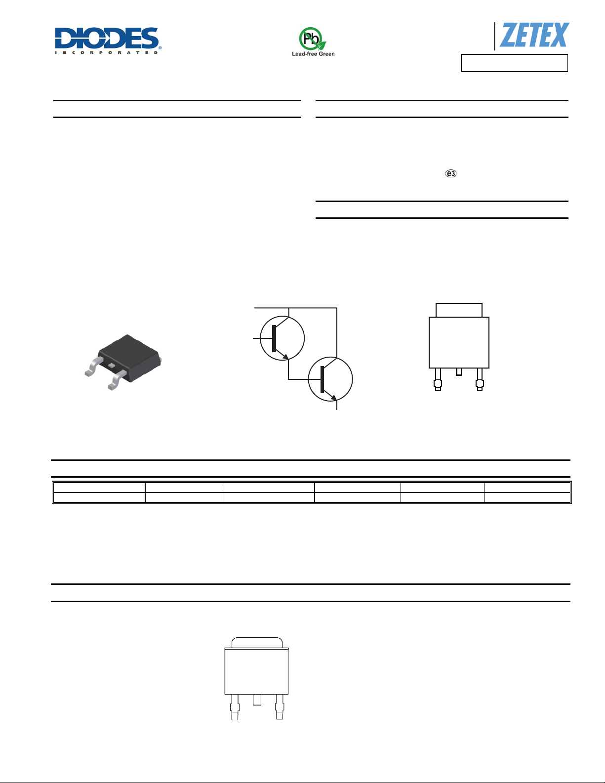
120V NPN MEDIUM POWER DARLINGTON TRANSISTOR IN TO252
Features
BV
BV
I
hFE > 2k for High Gain @ 1A
Totally Lead-Free & Fully RoHS Compliant (Notes 1 & 2)
Halogen and Antimony Free. “Green” Device (Note 3)
Qualified to AEC-Q101 Standards for High Reliability
> 120V
CEO
> 140V
CBO
= 1.5A High Continuous current
C
TO252 (DPAK)
Top View Top View
C
B
Mechanical Data
Case: TO252 (DPAK)
Case Material: Molded Plastic, "Green" Molding Compound.
Moisture Sensitivity: Level 1 per J-STD-020
Terminals: Finish - Matte Tin Plated Leads; Solderable
Weight: 0.34 grams (approximate)
Applications
DC Fans
Regulator Transistors
Relays
Solenoid Driving
Equivalent Circuit
Product Line o
Diodes Incorporated
ZXTN04120HK
UL Flammability Classification Rating 94V-0
per MIL-STD-202, Method 208
C
BE
E
Pin-Out
Ordering Information (Note 4)
Product Package Marking Reel size (inches) Tape width (mm) Quantity per reel
ZXTN04120HKTC TO252 (DPAK) ZXTN04120H 13 16 2,500
Notes: 1. No purposely added lead. Fully EU Directive 2002/95/EC (RoHS) & 2011/65/EU (RoHS 2) compliant.
2. See http://www.diodes.com/quality/lead_free.html for more information about Diodes Incorporated’s definitions of Halogen- and Antimony-free, "Green"
and Lead-free.
3. Halogen- and Antimony-free "Green” products are defined as those which contain <900ppm bromine, <900ppm chlorine (<1500ppm total Br + Cl) and
<1000ppm antimony compounds.
4. For packaging details, go to our website at http://www.diodes.com/products/packages.html
Marking Information
ZXTN04120HK
Document number: DS36554 Rev. 3 - 2
ZXTN
04120H
YYWW
www.diodes.com
ZXTN04120H = Product Type Marking Code
YYWW = Date Code Marking
YY = Last Digit of Year, (ex: 13 = 2013)
WW = Week Code 01 - 52
1 of 7
January 2014
© Diodes Incorporated
A
f
Product Line o
Diodes Incorporated
ZXTN04120HK
Absolute Maximum Ratings (@T
= +25°C, unless otherwise specified.)
A
Characteristic Symbol Value Unit
Collector-Base Voltage
Collector-Emitter Voltage
Emitter-Base Voltage
Continuous Collector Current
Peak Pulse Current
Thermal Characteristics (@T
= +25°C, unless otherwise specified.)
A
Characteristic Symbol Value Unit
(Note 5)
Power Dissipation
(Note 6) 2
(Note 7) 1.5
(Note 5)
Thermal Resistance, Junction to Ambient Air
(Note 6) 62.5
(Note 7) 80
Thermal Resistance, Junction to Leads (Note 8)
Thermal Resistance, Junction to Case (Note 9)
Operating and Storage Temperature Range
ESD Ratings (Note 10)
V
CBO
V
CEO
V
EBO
I
C
I
CM
140 V
120 V
14 V
1.5 A
4 A
3.9
P
D
W
32
R
θJA
°C/W
R
θJL
R
θJC
T
, T
J
STG
9
11
-55 to +150 °C
Electrostatic Discharge - Human Body Model ESD HBM 4,000 V 3A
Characteristic Symbol Value Unit JEDEC Class
Electrostatic Discharge - Machine Model ESD MM 400 V C
Notes: 5. For a device mounted with the exposed collector pad on 50mm x 50mm 2oz copper that is on a single-sided 1.6mm FR4 PCB; device is measured
7. Same as note (5), except mounted on minimum recommended pad (MRP) layout.
under still air conditions whilst operating in a steady-state.
6. Same as note (5), except mounted on 25mm x 25mm 1oz copper.
8. Thermal resistance from junction to solder-point (on the exposed collector pad).
9. Thermal resistance from junction to the top of the case.
10. Refer to JEDEC specification JESD22-A114 and JESD22-A115.
ZXTN04120HK
Document number: DS36554 Rev. 3 - 2
2 of 7
www.diodes.com
January 2014
© Diodes Incorporated
A
f
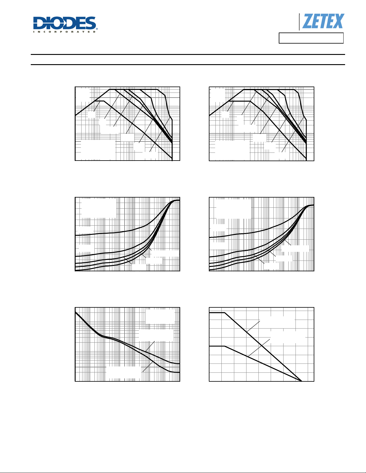
Thermal Characteristics and Derating Information
Product Line o
Diodes Incorporated
ZXTN04120HK
V
CE(sat)
Limit
1
DC
1s
100m
Collector Current (A)
C
I
10m
25mm x 25mm
100ms
T
=25°C
amb
1oz FR4
1 10 100
10ms
1ms
100µs
VCE Collector-Emitter Voltage (V)
Safe Operating Area
T
60
50
40
30
20
10
0
100µ 1m 10m 100m 1 10 100 1k
Thermal Resistance (°C/W)
=25°C
amb
25mm x 25mm
1oz FR4
D=0.5
D=0.2
Single Pulse
D=0.05
D=0.1
Pulse Width (s)
Transient Thermal Impedance
V
CE(sat)
Limit
1
DC
1s
100m
Collector Current (A)
C
I
10m
T
50mm x 50mm
100ms
=25°C
amb
2oz FR4
1 10 100
10ms
1ms
100µs
VCE Collector-Emitter Voltage (V)
Safe Operating Area
T
=25°C
30
20
10
0
100µ 1m 10m 100m 1 10 100 1k
Thermal Resistance (°C/W)
amb
50mm x 50mm
2oz FR4
D=0.5
D=0.2
Single Pulse
D=0.05
D=0.1
Pulse Width (s)
Transient Thermal Impedance
3 of 7
4.0
3.5
3.0
2.5
2.0
1.5
1.0
0.5
0.0
0 20 40 60 80 100 120 140 160
Max Power Dissipation (W)
Temperature (°C)
50mm x 50mm
2oz FR4
25mm x 25mm
1oz FR4
Derating Curve
January 2014
© Diodes Incorporated
Single Pulse
T
=25°C
100
10
25mm x 25mm
1
100µ 1m 10m 100m 1 10 100 1k
Max Power Dissipation (W)
1oz FR4
Pulse Width (s)
amb
50mm x 50mm
2oz FR4
Pulse Power Dissipation
ZXTN04120HK
Document number: DS36554 Rev. 3 - 2
www.diodes.com
 Loading...