Diodes ZXTD617MC User Manual

A
f
2
1
E
1
Product Line o
DUAL 15V NPN LOW SATURATION TRANSISTORS
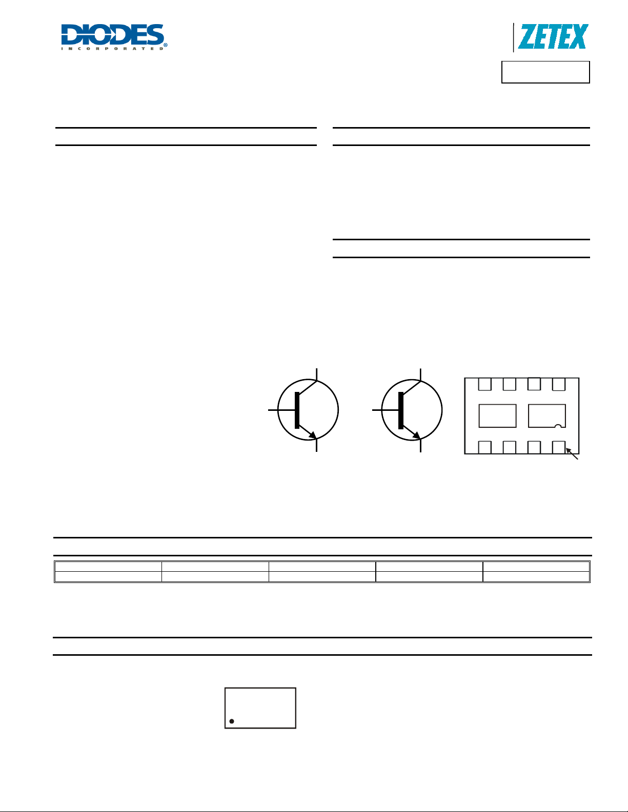
Features and Benefits
• BV
• I
• Low Saturation Voltage (100mV max @ 1A)
• R
• h
• Dual NPN saving footprint and component count
• Low profile 0.8mm high package for thin applications
• R
• 6mm
• Lead-Free, RoHS Compliant (Note 1)
• Halogen and Antimony Free. “Green” Device (Note 2)
• Qualified to AEC-Q101 Standards for High Reliability
Top View
> 15V
CEO
= 4.5A Continuous Collector Current
C
= 45 mΩ for a Low Equivalent On-Resistance
SAT
specified up to 12A for high current gain hold up
FE
efficient, 40% lower than SOT26
θJA
2
footprint, 50% smaller than TSOP6 and SOT26
DFN3020B-8
Bottom View
B2
NPN Transistor
Mechanical Data
• Case: DFN3020B-8
• Case Material: Molded Plastic. “Green” Molding Compound.
• Terminals: Pre-Plated NiPdAu leadframe
• UL Flammability Rating 94V-0
• Nominal Package Height: 0.8mm
• Moisture Sensitivity: Level 1 per J-STD-020
• Weight: 0.013 grams (approximate)
Applications
• DC-DC Converters
• Charging circuits
• Motor control
• Power switches
• Portable applications
C
B1
E2
NPN Transistor
Equivalent Circuit
Diodes Incorporated
C
C2 C2 C1 C1
C2
E2 B2 E1 B1
ZXTD617MC
C1
Pin 1
Bottom View
Pin-Out
Ordering Information
Product Marking Reel size (inches) Tape width (mm) Quantity per reel
ZXTD617MCTA DAA 7 8 3000
Notes: 1. No purposefully added lead.
2. Diodes Inc’s “Green” Policy can be found on our website at http://www.diodes.com
Marking Information
DAA
ZXTD617MC
Document Number DS31930 Rev. 3 - 2
DAA = Product type marking code
Top view, dot denotes pin 1
1 of 7
www.diodes.com
December 2010
© Diodes Incorporated

A
f
θ
Product Line o
Diodes Incorporated
ZXTD617MC
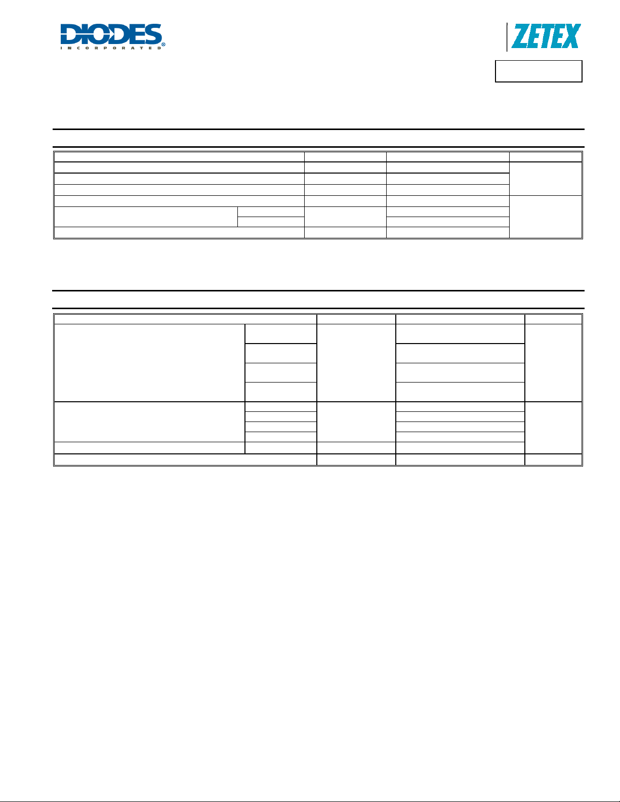
Maximum Ratings @T
= 25°C unless otherwise specified
A
Characteristic Symbol Value Unit
Collector-Base Voltage
Collector-Emitter Voltage
Emitter-Base Voltage
Peak Pulse Current
Continuous Collector Current
Base Current
V
CBO
V
CEO
V
EBO
I
(Notes 3 & 6)
(Notes 4 & 6) 5
CM
I
I
C
B
40
15
7
15
4.5
1
V
A
Thermal Characteristics @ T
= 25°C unless otherwise specified
A
Characteristic Symbol Value Unit
1.5
12
2.45
19.6
1.13
8
1.7
13.6
83.3
W
mW/°C
°C/W
Power Dissipation
Linear Derating Factor
Thermal Resistance, Junction to Ambient
(Notes 3 & 6)
(Notes 4 & 6)
P
D
(Notes 5 & 6)
(Notes 5 & 7)
(Notes 3 & 6)
(Notes 4 & 6) 51.0
(Notes 5 & 6) 111
R
JA
θ
(Notes 5 & 7) 73.5
Thermal Resistance, Junction to Lead (Notes 6 & 8)
Operating and Storage Temperature Range
Notes: 3. For a dual device surface mounted on 28mm x 28mm (8cm2) FR4 PCB with high coverage of single sided 2 oz copper, in still air conditions; the device is
measured when operating in a steady-state condition. The heatsink is split in half with the exposed collector pads connected to each half.
4. Same as note (3), except the device is measured at t <5 sec.
5. Same as note (3), except the device is surface mounted on 31mm x 31mm (10cm
6. For a dual device with one active die.
7. For dual device with 2 active die running at equal power.
8. Thermal resistance from junction to solder-point (at the end of the collector lead).
R
JL
, T
T
J
STG
2
) FR4 PCB with high coverage of single sided 1oz copper.
17.1
-55 to +150
°C
ZXTD617MC
Document Number DS31930 Rev. 3 - 2
2 of 7
www.diodes.com
December 2010
© Diodes Incorporated

A
f
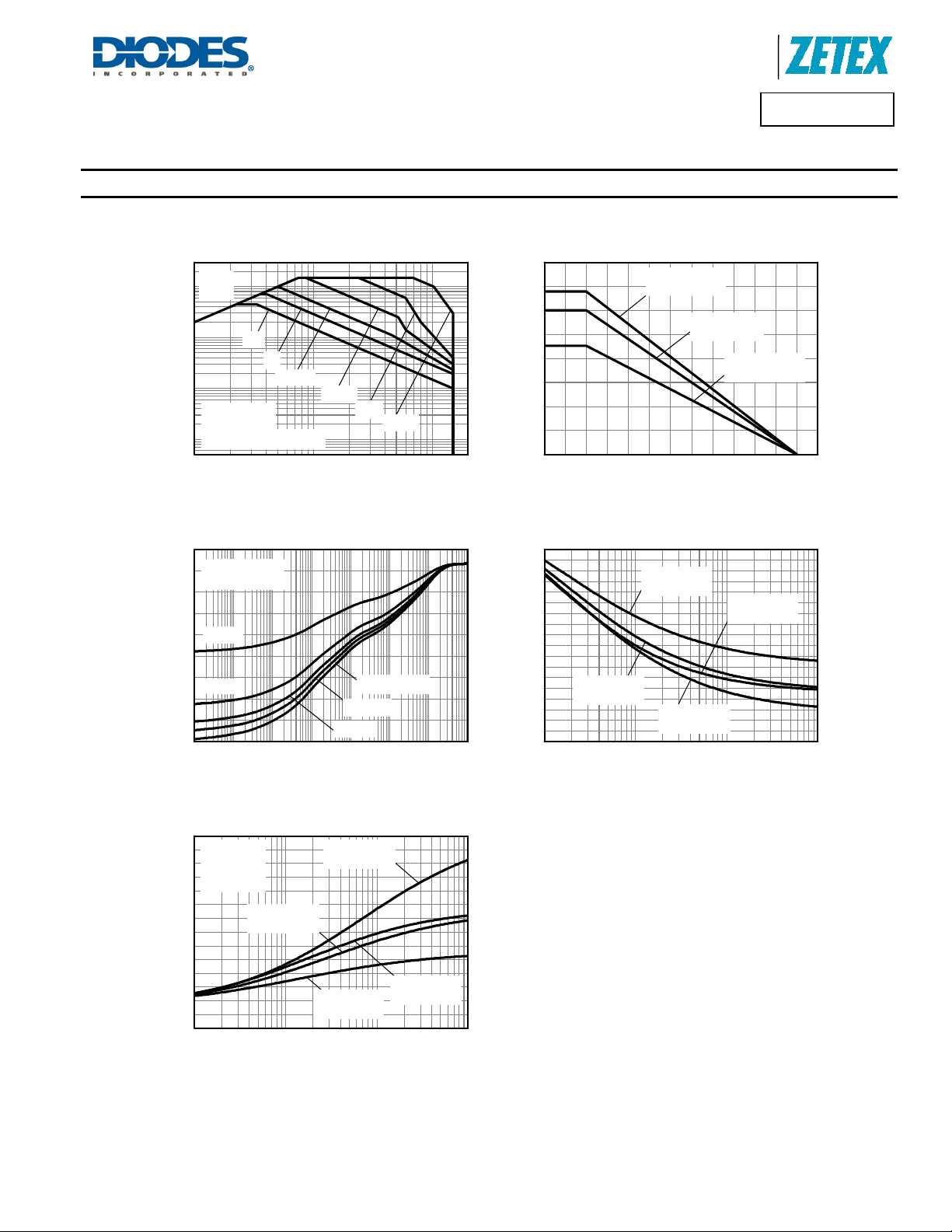
Thermal Characteristics
Product Line o
Diodes Incorporated
ZXTD617MC
V
CE(SAT)
10
Limited
0.01
Collector Current (A)
C
I
1
0.1
DC
8sqcm 2oz Cu
One active die
Single Pulse, T
1s
100ms
=25°C
amb
10ms
1ms
100us
0.1 1 10
VCE Collector-Emitter Voltage (V)
Safe Operating A rea
8sqcm 2oz Cu
80
One active die
60
D=0.5
40
D=0.2
20
Thermal Resistance (°C/W)
0
100µ 1m 10m 100m 1 10 100 1k
Single Pulse
D=0.05
D=0.1
Pulse Width (s)
Transient Thermal Impeda nc e
2.0
10sqcm 1oz Cu
Two active die
1.5
1.0
8sqcm 2oz Cu
One a ctive die
10sqcm 1oz Cu
One a ctive die
0.5
0.0
0 25 50 75 100 125 150
Max Power Dissipation (W)
Temperature (°C)
Derating Curve
225
200
175
150
1oz Cu
One active die
1oz Cu
Two active die
125
100
75
50
25
Thermal Resistance (°C/W)
2oz Cu
One active die
0
0.1 1 10 100
2oz Cu
Two active die
Board Cu Area (sqcm)
Thermal Resistance v B o ard A rea
3.5
3.0
2.5
2.0
T
=25°C
amb
T
=150°C
j max
Continuous
2oz Cu
One active die
2oz Cu
Two active die
1.5
1.0
Dissipation (W)
D
0.5
P
0.0
0.1 1 10 100
1oz Cu
One active die
1oz Cu
Two active die
Board Cu Area (sqcm)
Power Dissipation v Board Area
ZXTD617MC
Document Number DS31930 Rev. 3 - 2
3 of 7
www.diodes.com
December 2010
© Diodes Incorporated
 Loading...