Diodes ZXTC2061E6 User Manual

A
f
y
1
C
C
Features
Product Line o
Diodes Incorporated
ZXTC2061E6
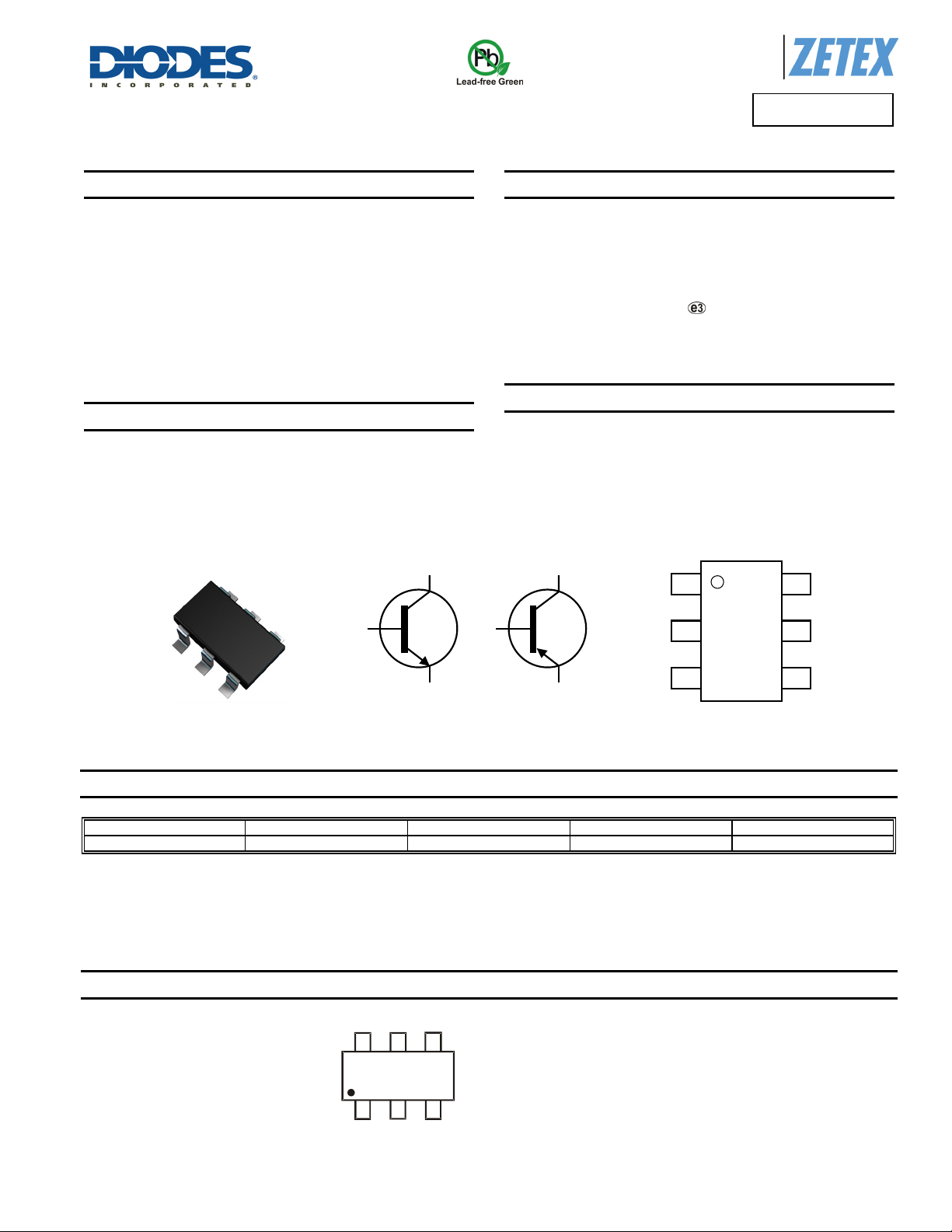
12V COMPLEMENTARY MEDIUM POWER TRANSISTOR IN SOT26
Mechanical Data
• NPN + PNP Combination
• BV
• BV
• Continuous Collector Current I
• V
• R
• Totally Lead-Free & Fully RoHS compliant (Notes 1 & 2)
• Halogen and Antimony Free. “Green” Device (Note 3)
• Qualified to AEC-Q101 Standards for High Reliability
> 12 (-12)V
CEO
> 7 (-7)V
EBO
< 32 (-70)mV @ 1A
CE(sat)
= 25 (45)mΩ
CE(sat)
= 5 (-3.5)A
C
Description
Advanced process capability has been used to achieve this high
performance device. Combining NPN and PNP transistors in the
SOT26 package provides a compact solution for the intended
applications.
ADVANCE INFORMATION
SOT26
B1
Q1
Top View
C
E1
Device S
• Case: SOT26
• Case Material: Molded Plastic, “Green” Molding Compound
• UL Flammability Classification Rating 94V-0
• Moisture Sensitivity: Level 1 per J-STD-020
• Terminals: Finish – Matte Tin Plated Leads, Solderable per
MIL-STD-202, Method 208
• Weight: 0.015 grams (approximate)
Applications
• MOSFET and IGBT Gate Driving
• Motor Drive
B2
mbol
Q2
C2
1
B1
2
E2
Top View
Pin-Out
E1
B2
E2
Ordering Information (Note 4)
Product Marking Reel size (inches) Tape width (mm) Quantity per reel
ZXTC2061E6TA 2061 7 8 3,000
Notes: 1. No purposely added lead. Fully EU Directive 2002/95/EC (RoHS) & 2011/65/EU (RoHS 2) compliant.
2. See http://www.diodes.com/ for more information about Diodes Incorporated’s definitions of Halogen and Antimony free, "Green" and Lead-Free.
3. Halogen and Antimony free "Green” products are defined as those which contain <900ppm bromine, <900ppm chlorine (<1500ppm total Br + Cl) and
<1000ppm antimony compounds.
4. For packaging details, go to our website at http://www.diodes.com
Marking Information
ZXTC2061E6
Document Number: DS33646 Rev: 2 - 2
2061
www.diodes.com
2061 = Product Type Marking Code
1 of 9
February 2013
© Diodes Incorporated

A
f
Product Line o
Diodes Incorporated
ZXTC2061E6
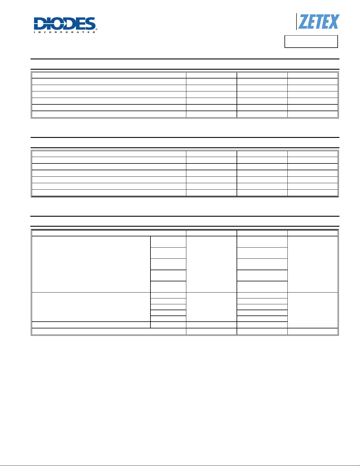
Maximum Ratings – Q1 (NPN Transistor) (@T
= +25°C, unless otherwise specified.)
A
Characteristic Symbol Value Unit
Collector-Base Voltage
Collector-Emitter Voltage
Emitter-Base Voltage
Continuous Collector Current
Peak Pulsed Collector Current
Base Current
V
CBO
V
CEO
V
EBO
I
C
I
CM
I
B
20 V
12 V
7 V
5 A
12 A
1 A
Maximum Ratings – Q2 (PNP Transistor) (@T
= +25°C, unless otherwise specified.)
A
Characteristic Symbol Value Unit
Collector-Base Voltage
Collector-Emitter Voltage
Emitter-Base Voltage
Continuous Collector Current
Peak Pulsed Collector Current
Base Current
ADVANCE INFORMATION
V
CBO
V
CEO
V
EBO
I
C
I
CM
I
B
-12 V
-12 V
-7 V
-3.5 A
-10 A
-1 A
Thermal Characteristics (@T
= +25°C, unless otherwise specified.)
A
Characteristic Symbol Value Unit
0.7
5.6
0.9
7.2
1.1
8.8
1.1
8.8
1.7
13.6
179
Power Dissipation
Linear Derating Factor
(Notes 5 & 9)
(Notes 6 & 9)
(Notes 6 & 10)
(Notes 7 & 9)
(Notes 8 & 9)
(Notes 5 & 9)
P
D
(Notes 6 & 9) 139
Thermal Resistance, Junction to Ambient
(Notes 6 & 10) 113
R
θJA
(Notes 7 & 9) 113
(Notes 8 & 9) 73
Thermal Resistance, Junction to Lead (Note 11)
Operating and Storage Temperature Range
Notes: 5. For a device surface mounted on 15mm x 15mm FR4 PCB with high coverage of single sided 1oz copper, in still air conditions; the device is measured
when operating in a steady-state condition.
6. Same as note (5), except the device is surface mounted on 25mm x 25mm 1oz copper.
7. Same as note (5), except the device is surface mounted on 50mm x 50mm 2oz copper.
8. Same as note (7), except the device is measured at t < 5 seconds.
9. For device with one active die, both collectors attached to a common heatsink.
10. For device with two active dice running at equal power, split heatsink 50% to each collector.
11. Thermal resistance from junction to solder-point (at the end of the collector lead).
R
θJL
T
, T
J
STG
87.58
-55 to +150 °C
W
mW/°C
°C/W
ZXTC2061E6
Document Number: DS33646 Rev: 2 - 2
2 of 9
www.diodes.com
February 2013
© Diodes Incorporated

A
f
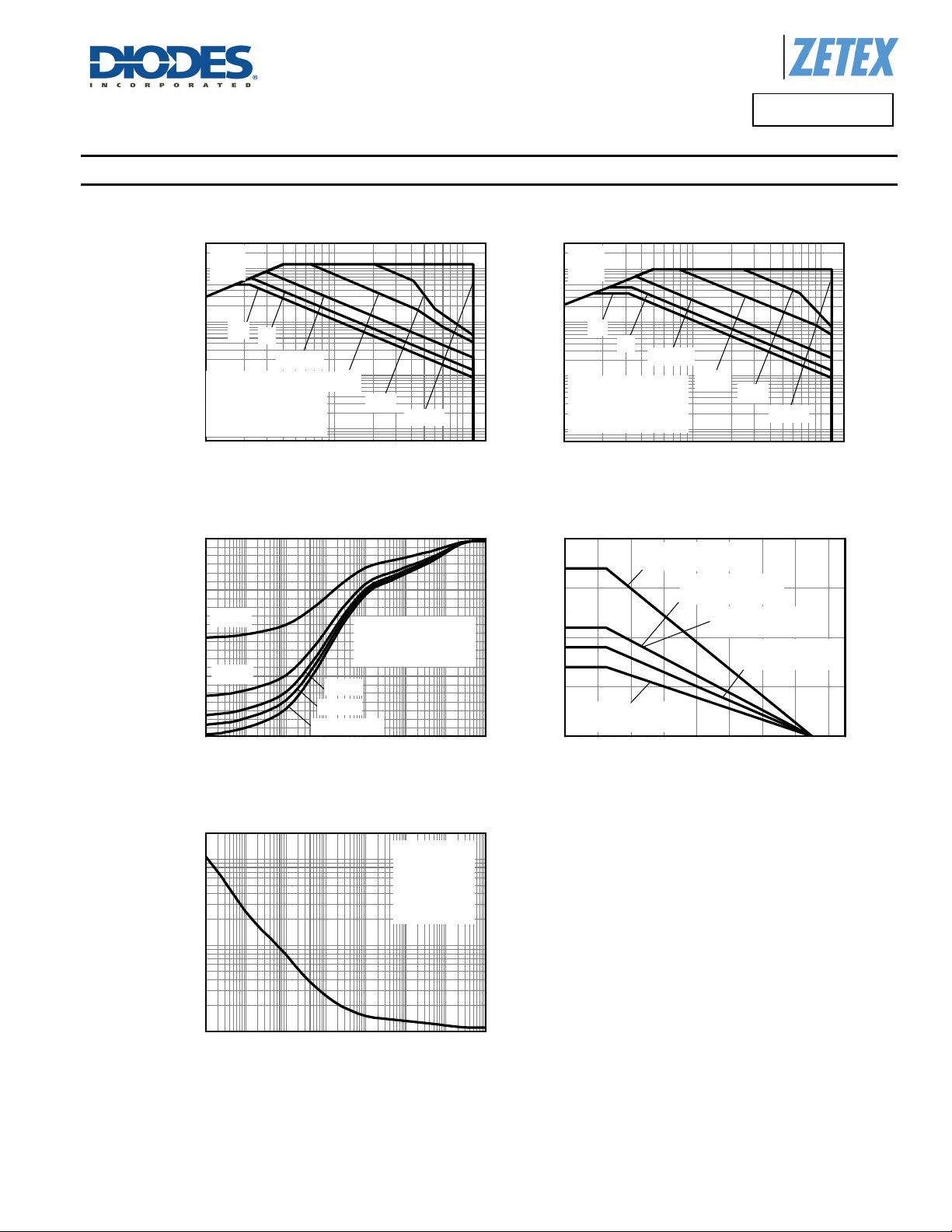
Thermal Characteristics and Derating Information
Product Line o
Diodes Incorporated
ZXTC2061E6
R
DS(on)
10
Limit
1
DC
1s
T
amb
NPN
=25°C
100ms
10ms
1ms
100µs
Collector Current (A)
-I
100m
50mm x 50mm 2oz FR4
Collector Current (A)
I
10m
C
One active die
100m 1 10
VCE Collector-Emitter Voltage (V)
Safe Operating Area
ADVANCE INFORMATION
110
100
90
80
70
D=0.5
60
50
40
D=0.2
30
20
10
0
100µ 1m 10m 100m 1 10 100 1k
Thermal Resistance (°C/W)
D=0.1
D=0.05
Single Pulse
Pulse Width (s)
T
=25°C
amb
50mm x 50mm 2oz FR4
One activ die
Transient Thermal Impedance
R
DS(on)
10
Limit
1
DC
1s
100ms
100m
50mm x 50mm 2oz FR4
10m
C
PNP
T
=25°C
amb
One active die
10ms
1ms
0.1 1 10
-VCE Collector-Emitter Voltage (V)
Safe Operating Area
2.0
1.5
1.0
0.5
15mm x 15mm 1oz FR4
0.0
0 20 40 60 80 100 120 140 160
Max Power Dissipation (W)
50mm x 50mm 2oz FR4
One activ die, t < 5 sec
25mm x 25mm 1oz FR4
two activ die
50mm x 50mm 2oz FR4
One activ die
25mm x 25mm 1oz FR4
One activ die
Temperature (°C)
Derating Curve
100µs
One activ die
100
Single Pulse
T
=25°C
amb
50mm x 50mm
2oz FR4
One active die
10
1
100µ 1m 10m 100m 1 10 100 1k
Max Power Dissipation (W)
Pulse Width (s)
Pulse Power Dissipation
ZXTC2061E6
Document Number: DS33646 Rev: 2 - 2
3 of 9
www.diodes.com
February 2013
© Diodes Incorporated
 Loading...