

Page 1
ZXT790AK
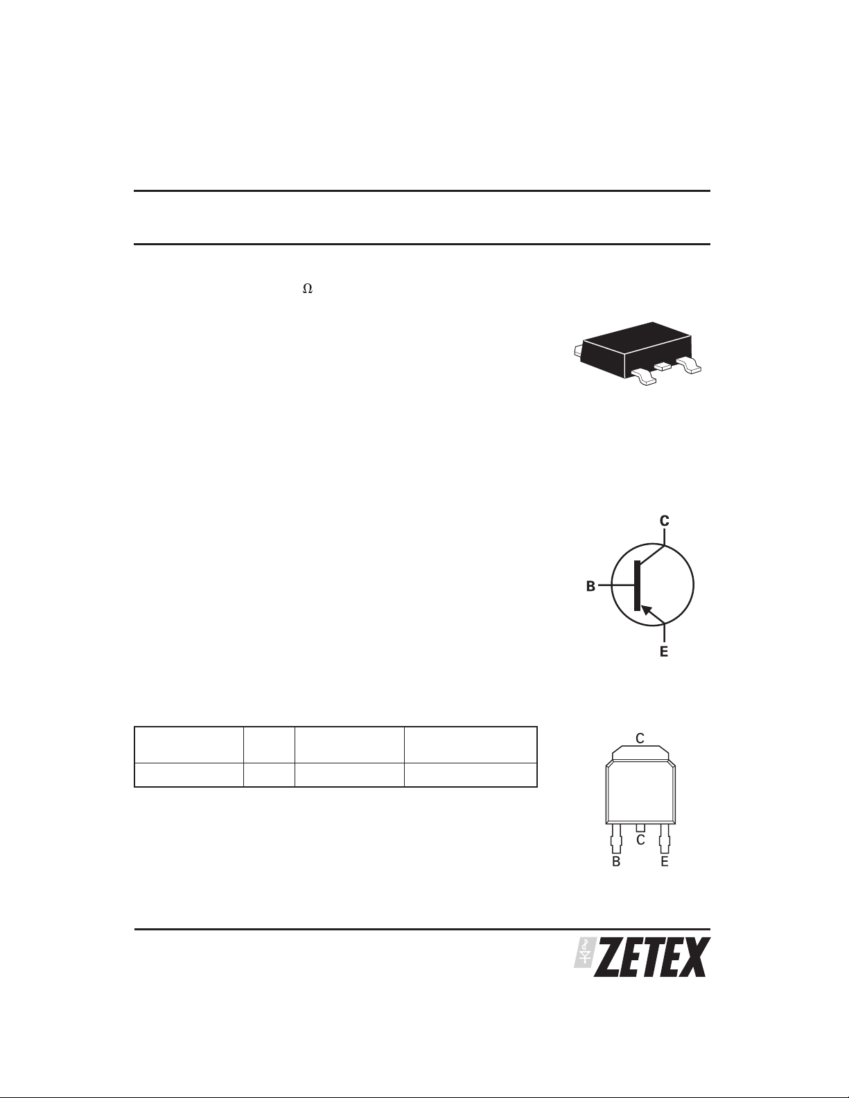
40V PNP MEDIUM POWER HIGH GAIN TRANSISTOR IN D-PAK
SUMMARY
CEO
= -40V : R
BV
DESCRIPTION
Packaged in the D-Pak outline this high gain 40V PNP transistor offers low on state
losses making it ideal for use in DC-DC circuits and various driving and power
management functions.
= 83m ; IC= -3A
SAT
FEATURES
3 Amps continuous current
•
Up to 6 Amps peak current
•
Low saturation voltages
•
High gain
•
APPLICATIONS
•
DC - DC Converters
•
MOSFET gate drivers
•
Charging circuits
•
Power switches
•
Siren drivers
ORDERING INFORMATION
DEVICE REEL
SIZE
ZXT790AKTC 13" 16mm embossed 2500 units
TAPE WIDTH QUANTITY PER REEL
K
A
P
D
PINOUT
DEVICE MARKING
•
ZXT790A
ISSUE 1 - JUNE 2003
1
SEMICONDUCTORS
Page 2
ZXT790AK
ABSOLUTE MAXIMUM RATINGS
PARAMETER SYMBOL LIMIT UNIT
Collector-Base Voltage BV
Collector-Emitter Voltage BV
Emitter-Base Voltage BV
Continuous Collector Current I
Peak Pulse Current I
Base Current I
Power Dissipation at TA =25°C
(a)
CBO
CEO
EBO
C
CM
B
P
D
Linear Derating Factor
Thermal Resistance Junction to Ambient
Power Dissipation at TA =25°C
(b)
P
D
Linear Derating Factor
Thermal Resistance Junction to Ambient
Power Dissipation at TA =25°C
(c)
P
D
Linear Derating Factor
Thermal Resistance Junction to Ambient
Operating and Storage Temperature Range T
j,Tstg
NOTES
(a) For a device surface mounted on 25mm x 25mm FR4 PCB with high coverage of single sided 1oz copper, in still
air conditions.
(b) For a device surface mounted on 50mm x 50mm FR4 PCB with high coverage of single sided 1oz copper in still
air conditions.
(c) For a device surface mounted on 50mm x 50mm FR4 PCB with high coverage of single sided 2oz copper in still
air conditions.
-50 V
-40 V
-5 V
-3 A
-6 A
-0.5 A
2.1
16.8
59
mW/°C
°C/W
3.0
24.4
41
mW/°C
°C/W
3.9
30.9
32
mW/°C
°C/W
-55 to 150 °C
W
W
W
SEMICONDUCTORS
ISSUE 1 - JUNE 2003
2
Page 3

CHARACTERISTICS
ZXT790AK
ISSUE 1 - JUNE 2003
3
SEMICONDUCTORS
Page 4

ZXT790AK
ELECTRICAL CHARACTERISTICS (at T
= 25°C unless otherwise stated)
amb
PARAMETER SYMBOL MIN. TYP. MAX. UNIT CONDITIONS
Collector-Base Breakdown Voltage BV
Collector-Emitter Breakdown Voltage BV
Emitter-Base Breakdown Voltage BV
Collector Cut-Off Current I
Collector Cut-Off Current I
Emitter Cut-Off Current I
Collector-Emitter Saturation Voltage V
Base-Emitter Saturation Voltage V
Base-Emitter Turn-On Voltage V
Static Forward Current Transfer Ratio h
Transition Frequency f
CBO
CEO
EBO
CBO
S <1 -20 nA VCB= -30V
CE
EBO
CE(SAT)
BE(SAT)
BE(ON)
FE
T
-50 -70 V IC= -100A
-40 -60 V IC= -10mA
-5 -8.3 V IE= -100A
<1 -20 nA VCB= -30V
<1 -20 nA VEB= -4V
-110
-170
mV
IC= -0.5A, IB= -5mA
-220
-260
-250
-350
-450
-450
IC= -1A, IB= -10mA
mV
IC= -2A, IB= -50mA
mV
IC= -3A, IB= -300mA
mV
-1.05 -1.15 V IC= -3A, IB = -300mA
-0.9 -1.0 V IC= -3A, VCE = -2V
300
450
800 IC= -10mA, VCE= -2V
250
200
150
80
390
350
280
170
IC= -500mA, VCE= -2V
IC= -1A, VCE= -2V
IC= -2A, VCE= -2V
IC= -3A, VCE= -2V
100 MHz IC= -50mA, VCE= -5V
f = 50MHz
Output Capacitance C
Switching Times t
t
OBO
ON
OFF
24 pF VCB= -10V, f = 1MHz
35
600
nsnsIC= -500mA, VCC= -10V,
I
B1=IB2
= -50mA
(1)
(1)
(1)
(1)
(1)
(1)
(1)
(1)
(1)
(1)
(1)
(1)
(1)
NOTES
(1) Measured under pulsed conditions. Pulse width ⱕ 300s; duty cycle ⱕ 2%.
SEMICONDUCTORS
4
ISSUE 1 - JUNE 2003
Page 5

TYPICAL CHARACTERISTICS
ZXT790AK
ISSUE 1 - JUNE 2003
5
SEMICONDUCTORS
Page 6

ZXT790AK
PACKAGE OUTLINE
Controlling dimensions are in millimetres.
Approximate conversions are given in inches
DIM MILLIMETRES INCHES
MIN MAX MIN MAX
A 2.18 2.38 0.086 0.094
A1 ᎏ 0.127 ᎏ 0.005
b 0.635 0.89 0.025 0.035
b2 0.762 1.114 0.030 0.045
b3 5.20 5.46 0.205 0.215
c 0.457 0.609 0.018 0.024
c2 0.457 0.584 0.018 0.023
D 5.97 6.22 0.235 0.245
D1 5.20 ᎏ 0.205 ᎏ
E 6.35 6.73 0.250 0.265
E1 4.32 ᎏ 0.170 ᎏ
e 2.30 BSC 0.090 BSC
H 9.40 10.41 0.370 0.410
L 1.40 1.78 0.055 0.070
L1 2.74 REF 0.108 REF
L2 0.051 BSC 0.020 BSC
L3 0.89 1.27 0.035 0.050
L4 0.635 1.01 0.025 0.040
L5 1.14 1.52 0.045 0.060
⍜1⬚ 0ⴗ 10ⴗ 0ⴗ 10ⴗ
⍜⬚ 0ⴗ 15ⴗ 0ⴗ 15ⴗ
© Zetex plc 2003
Europe
Zetex plc
Fields New Road
Chadderton
Oldham, OL9 8NP
United Kingdom
Telephone (44) 161 622 4444
Fax: (44) 161 622 4446
hq@zetex.com
These offices are supported by agents and distributors in major countries world-wide.
This publicationis issued toprovide outline informationonly which (unlessagreed by theCompany in writing)may not be used,applied or reproduced
for any purpose or form part of any order or contract or be regarded as a representation relating to the products or services concerned. The Company
reserves the right to alter without notice the specification, design, price or conditions of supply of any product or service.
For the latest product information, log on to
Zetex GmbH
Streitfeldstraße 19
D-81673 München
Germany
Telefon: (49) 89 45 49 49 0
Fax: (49) 89 45 49 49 49
europe.sales@zetex.com
www.zetex.com
Americas
Zetex Inc
700 Veterans Memorial Hwy
Hauppauge, NY 11788
USA
Telephone: (1) 631 360 2222
Fax: (1) 631 360 8222
usa.sales@zetex.com
Asia Pacific
Zetex (Asia) Ltd
3701-04 Metroplaza Tower 1
Hing Fong Road
Kwai Fong
Hong Kong
Telephone: (852) 26100 611
Fax: (852) 24250 494
asia.sales@zetex.com
ISSUE 1 - JUNE 2003
SEMICONDUCTORS
6
 Loading...