Diodes ZXT13P40DE6 User Manual

A
f
y
C
Product Line o
Diodes Incorporated
ZXT13P40DE6
Features
• BV
• I
• I
• R
• Low Saturation Voltage (-200mV max @ 1A)
• h
• Totally Lead-Free & Fully RoHS compliant (Notes 1 & 2)
• Halogen and Antimony Free. “Green” Device (Note 3)
• Qualified to AEC-Q101 Standards for High Reliability
• PPAP capable (Note 4)
ADVANCE INFORMATION
> -40V
CEO
= -3A Max Continuous Collector Current
C
= -10A Peak Pulse Current
CM
= 58mΩ for a low equivalent On-Resistance
CE(SAT)
characterized up to -5A for high current gain hold up
FE
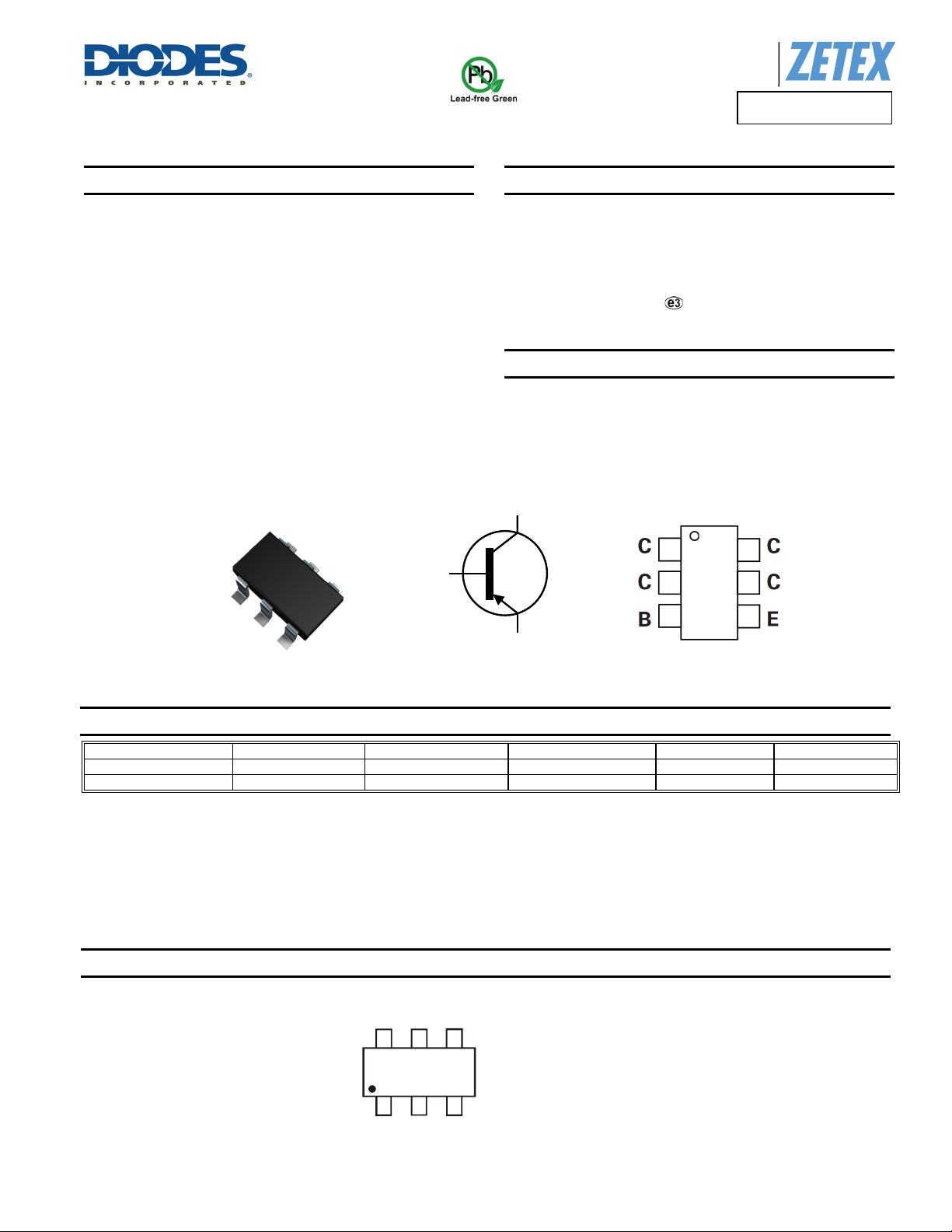
SOT26
Top View
40V PNP LOW SATURATION SWITCHING TRANSISTOR IN SOT26
Mechanical Data
• Case: SOT26
• Case Material: Molded Plastic, “Green” Molding Compound. UL
Flammability Classification Rating 94V-0
• Moisture Sensitivity: Level 1 per J-STD-020
• Terminals: Finish – Matte Tin Plated Leads, Solderable per MIL-
STD-202, Method 208
• Weight: 0.015 grams (approximate)
Applications
• DC - DC Converters
• Power Management Functions
• Power Switches
• Motor Control
B
E
Device S
mbol
Pin-Out Top
Ordering Information (Notes 4 & 5)
Product Compliance Marking Reel size (inches) Tape width (mm) Quantity per reel
ZXT13P40DE6TA AEC-Q101 P40D 7 8 3,000
ZXT13P40DE6QTA Automotive P40D 7 8 3,000
Notes: 1. No purposely added lead. Fully EU Directive 2002/95/EC (RoHS) & 2011/65/EU (RoHS 2) compliant.
2. See http://www.diodes.com/quality/lead_free.html for more information about Diodes Incorporated’s definitions of Halogen- and Antimony-free, "Green"
and Lead-free.
3. Halogen- and Antimony-free "Green” products are defined as those which contain <900ppm bromine, <900ppm chlorine (<1500ppm total Br + Cl) and
<1000ppm antimony compounds.
5. For packaging details, go to our website at http://www.diodes.com/products/packages.html.
4. Automotive products are AEC-Q101 qualified and are PPAP capable. Automotive, AEC-Q101 and standard products are electrically and thermally
the same, except where specified. For more information, please refer to http://www.diodes.com/quality/product_compliance_definitions/.
Marking Information
ZXT13P40DE6
Document Number: DS33639 Rev: 4 - 2
P40D
www.diodes.com
P40D = Product Type Marking Code
1 of 7
May 2014
© Diodes Incorporated

A
f
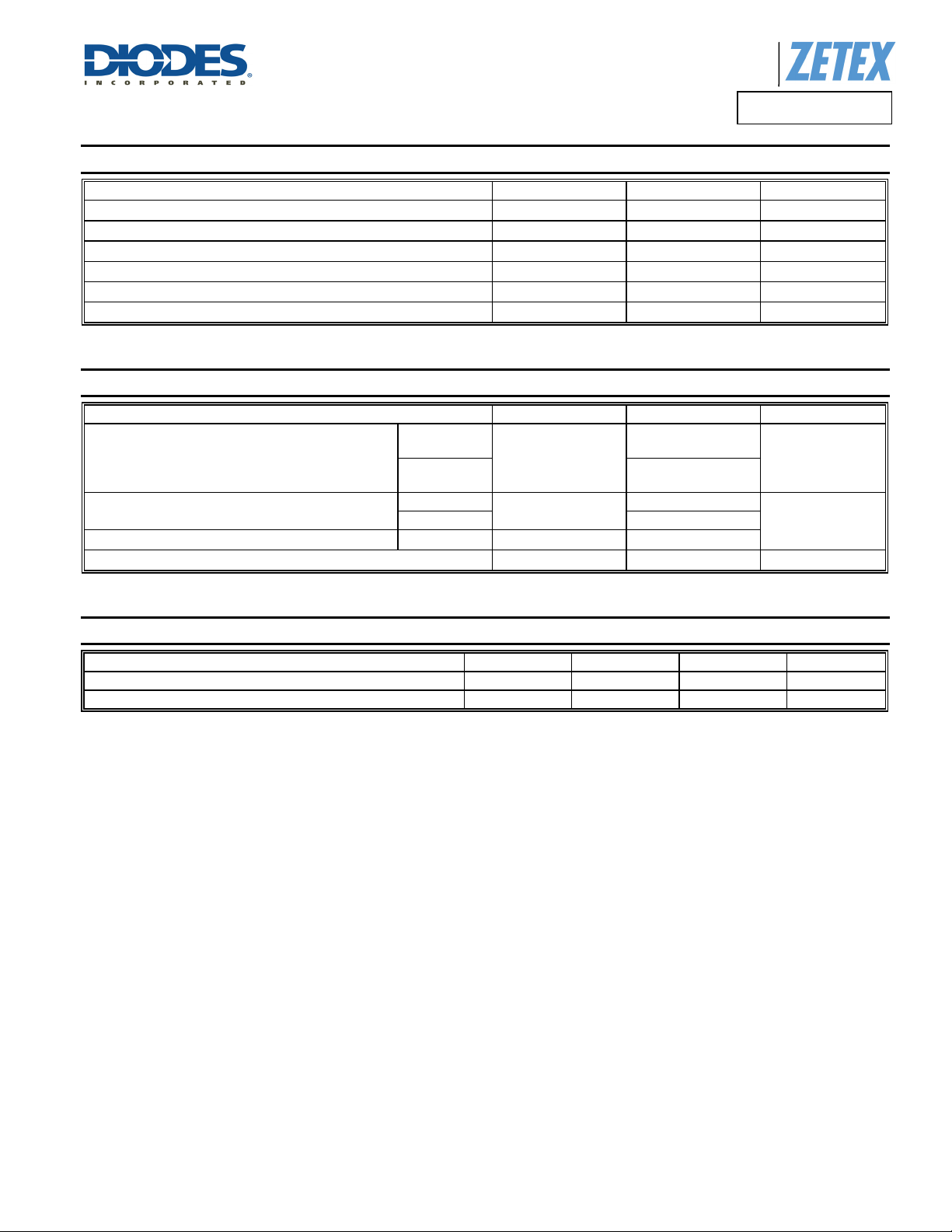
Absolute Maximum Ratings (@T
Characteristic Symbol Value Unit
Collector-Base Voltage
Collector-Emitter Voltage
Emitter-Base Voltage
Base Current
Continuous Collector Current
Peak Pulse Collector Current
Thermal Characteristics (@T
Characteristic Symbol Value Unit
Power Dissipation
Linear Derating Factor
Thermal Resistance, Junction to Ambient
ADVANCE INFORMATION
Thermal Resistance, Junction to Lead (Note 8)
Operating and Storage Temperature Range
A
= +25°C, unless otherwise specified.)
A
ESD Ratings (Note 9)
= +25°C, unless otherwise specified.)
V
CBO
V
CEO
V
EBO
I
B
I
C
I
CM
(Note 6)
P
(Note 7)
(Note 6)
(Note 7) 73
D
R
θJA
R
θJL
T
, T
J
STG
Product Line o
Diodes Incorporated
ZXT13P40DE6
-50 V
-40 V
-7.5 V
-500 mA
-3 A
-10 A
1.1
8.8
1.7
13.6
113
18.61
-55 to +150
W
mW/°C
°C/W
°C
Characteristic Symbol Value Unit JEDEC Class
Electrostatic Discharge - Human Body Model ESD HBM 4,000 V 3A
Electrostatic Discharge - Machine Model ESD MM 400 V C
Notes: 6. For a device mounted with collector leads on 25mm x 25mm 1oz copper that is on a single-sided 1.6mm FR4 PCB; device is measured under still air
conditions whilst operating in a steady-state.
7. Same as note (6), except the device is measured at t ≤ 5secs.
8. Thermal resistance from junction to solder-point (at the end of the collector leads).
9. Refer to JEDEC specification JESD22-A114 and JESD22-A115.
ZXT13P40DE6
Document Number: DS33639 Rev: 4 - 2
2 of 7
www.diodes.com
May 2014
© Diodes Incorporated

A
f
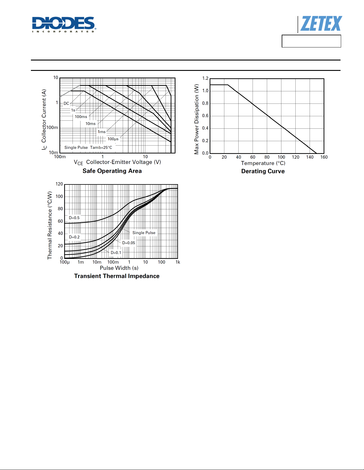
Thermal Characteristics and Derating Information
ADVANCE INFORMATION
Product Line o
Diodes Incorporated
ZXT13P40DE6
ZXT13P40DE6
Document Number: DS33639 Rev: 4 - 2
3 of 7
www.diodes.com
May 2014
© Diodes Incorporated
 Loading...