Diodes ZLLS1000 User Manual

A
f
Features
• Low Equivalent on Resistance
• Extremely Low Leakage (typically 6μA @30V)
• High current capability (I
• Low V
• SOT23 Package
• ZLLS1000 Complements Low Temperature Equivalent
• Package Thermally Rated to +150°C
• Totally Lead-Free & Fully RoHS Compliant (Notes 1 & 2)
• Halogen and Antimony Free. “Green” Device (Note 3)
• Qualified to AEC-Q101 Standards for High Reliability
, Fast Switching Schottky
F
ZHCS1000
= 1.16A)
F
SOT23
Top View
Product Line o
Diodes Incorporated
ZLLS1000
40V HIGH CURRENT LOW LEAKAGE SCHOTTKY DIODE
Mechanical Data
• Case: SOT23
• UL Flammability Rating 94V-0
• Moisture Sensitivity: Level 1 per J-STD-020
• Terminals: Matte Tin Finish
• Weight: 0.008 grams (Approximate)
Applications
• DC – DC Converters
• Strobes
• Mobile Phones
• Charging Circuits
• Motor Control
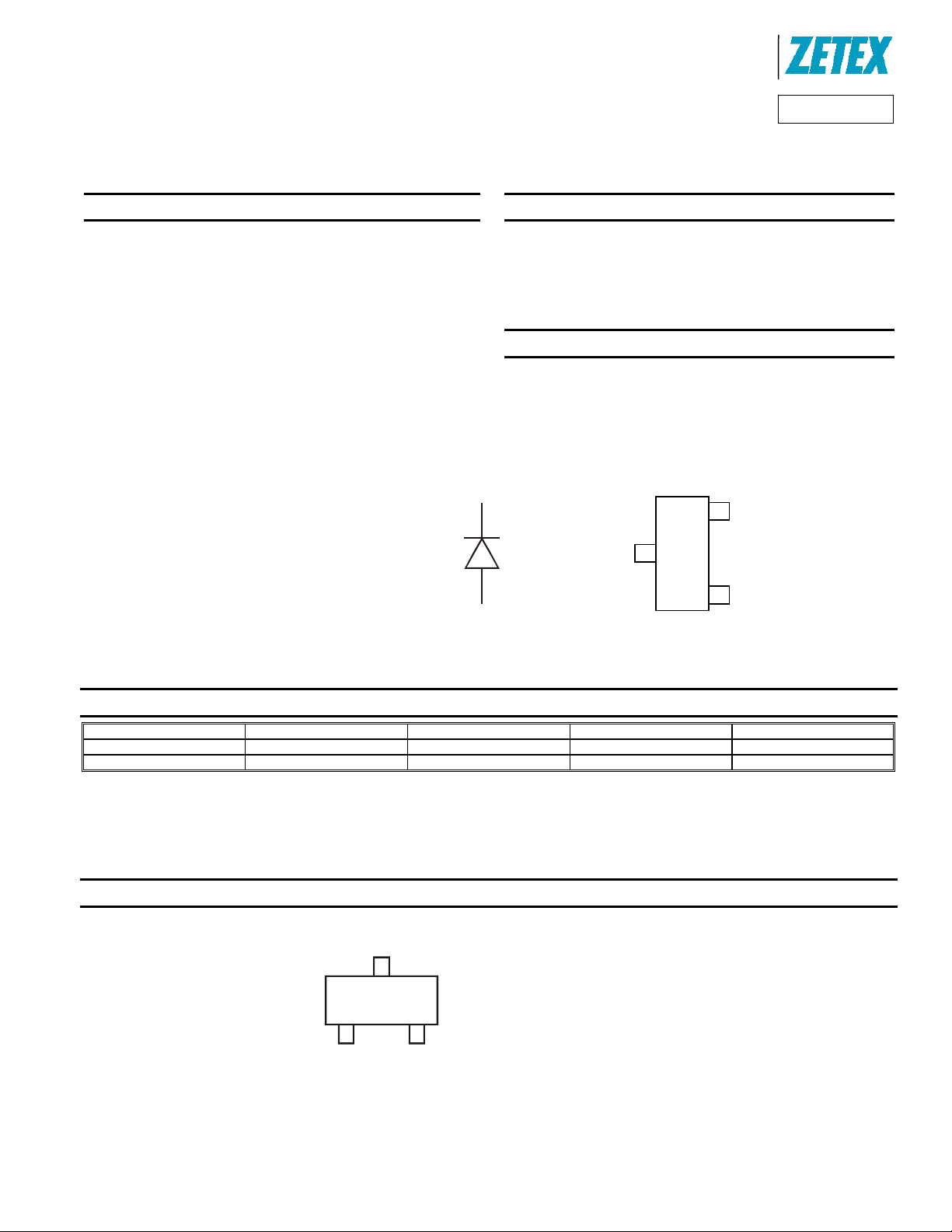
Cathode
N/C
C
A
Anode
Device Symbol
Pinout – Top View
Ordering Information
Product Marking Reel size (inches) Tape width (mm) Quantity per reel
ZLLS1000TA L10 7 8 3,000 units
ZLLS1000TC L10 13 8 10,000 units
Notes: 1. No purposely added lead. Fully EU Directive 2002/95/EC (RoHS) & 2011/65/EU (RoHS 2) compliant.
2. See http://www.diodes.com for more information about Diodes Incorporated’s definitions of Halogen- and Antimony-free, "Green" and Lead-free.
3. Halogen- and Antimony-free "Green” products are defined as those which contain <900ppm bromine, <900ppm chlorine (<1500ppm total Br + Cl) and
<1000ppm antimony compounds.
Marking Information
L10
ZLLS1000
Document Number DS32021 Rev. 6 - 2
L10 = Product type Marking Code
1 of 6
www.diodes.com
July 2012
© Diodes Incorporated

A
f
Product Line o
Diodes Incorporated
ZLLS1000
Maximum Ratings (@T
Characteristic Symbol Value Unit
Continuous Reverse Voltage
Forward Current
Peak Repetitive Forward Current
Rectangular Pulse Duty Cycle 50% 100μs pulse width
Non Repetitive Forward Current t≤100μs
t≤10ms
= +25°C, unless otherwise specified.)
A
V
R
I
F
I
FPK
I
FSM
40 V
1.16 A
2.6 A
22
6.4
Thermal Characteristics
Characteristic Symbol Value Unit
Power Dissipation @TA = +25°C Single Die Continuous
Single Die Measured at t<5 secs
Thermal Resistance Junction to Ambient (Note 4)
Thermal Resistance Junction to Ambient (Note 5)
Thermal Resistance Junction to Lead (Solder Point)
Storage temperature range
Junction temperature
Notes: 4. For a device surface mounted on 25mm x 25mm FR4 PCB with high coverage of single sided 1oz copper, in still air conditions.
5. For a device mounted on FRB PCB measured at t<5secs.
R
R
R
T
P
θJA
θJA
θJL
STG
T
D
J
0.8
1.18
155 °C/W
106 °C/W
80 °C/W
-55 to +150 °C
150 °C
A
A
W
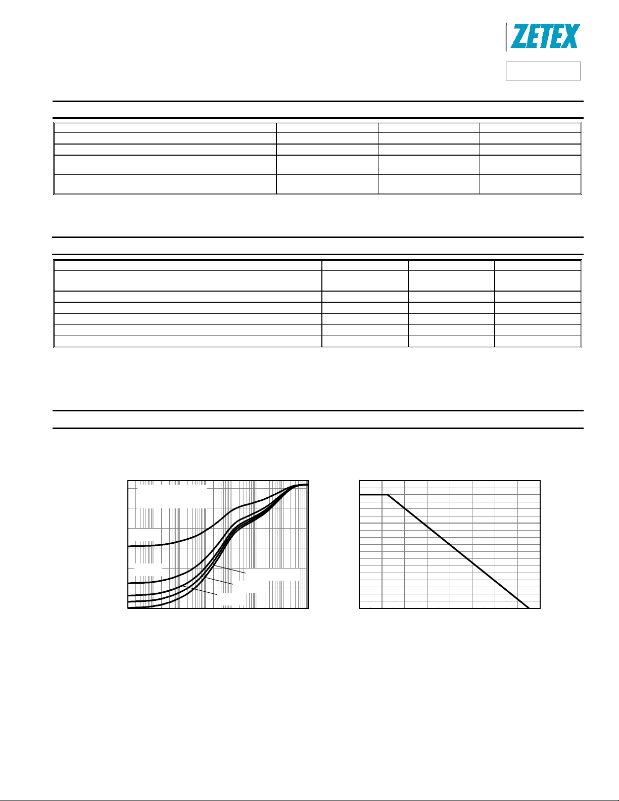
Thermal Characteristics and Derating information
150
100
T
=25°C
amb
Rectangular Pulse
D=0.5
0.9
0.8
0.7
0.6
0.5
0.4
50
D=0.2
0
100µ 1m 10m 100m 1 10 100 1k
Thermal Resistance (°C/W)
D=0.1
Single Pulse
D=0.05
0.3
0.2
0.1
0.0
Max Power Di ssi p ation (W)
Pulse Width (s )
Transient Thermal Impedance
0 20 40 60 80 100 120 140 160
Temperature (°C)
Derating Curve
ZLLS1000
Document Number DS32021 Rev. 6 - 2
2 of 6
www.diodes.com
July 2012
© Diodes Incorporated
 Loading...