Diodes ZLDO485 User Manual

4.85 VOLT ULTRA LOW DROPOUT
REGULATOR
ISSUE 2 - MAY 1997
ZLDO485
DEVICE DESCRIPTION
The ZLDO Series low dropout linear
regulators operate with an exceptionally
low dropout voltage, typically only 30mV
with a load current of 100mA. The regulator
series features output voltages in the range
2.7 to 18 volts, this device provides an output
voltage of 4.85 volts.
The ZLDO485 consumes a typical quiescent
current of only 1mA and is rated to supply
load currents up to 300mA. A battery low flag
is available to indicate potential power fail
situations. If the input voltage falls to within
200mV of the regulated output voltage then
the error output pulls low. The device also
features an active high disable control. Once
disabled the ZLDO quiescent current falls to
typically 11µA.
The ZLDO devices are packaged in Zetex
SM8 8 pin small outline surface mount
package, ideal for applications where space
saving is important. The device low dropout
voltage, low quiescent current and small size
make it ideal for low power and battery
powered applications. Battery powered
circuits can make particular use of the low
battery flag and shutdown features.
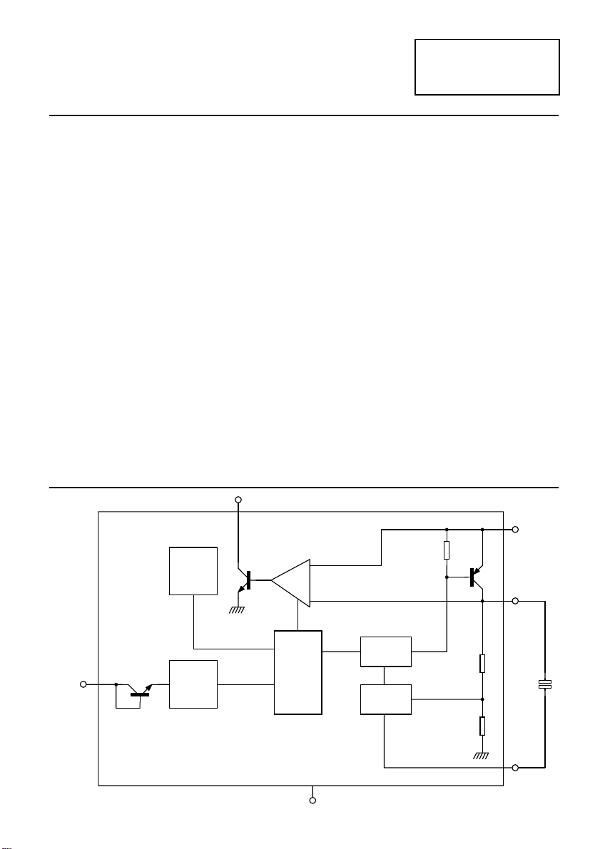
THERMAL
SHUTDOWN
Low Battery Flag
FEATURES
•
•
•
•
•
•
•
•
•
•
•
APPLICATIONS
•
•
•
•
•
LOW BATTERY
COMPARATOR
Very low dropout voltage
6mV dropout at 10mA output
30mV dropout at 100mA output
100mV dropout at 300mA output
4.85 volt fixed output
Other voltages available
Low quiescent current
1mA quiescent (typ) at 300mA output
Low battery flag
Shutdown control
Surface mount package
Battery powered devices
Portable instruments
Portable communications
Laptop/Palmtop computers
Electronic organisers
Vin
Vo
Shutdown
Control
SHUTDOWN
BIAS
CIRCUIT
4-71
Gnd
OUTPUT
DRIVE
BANDGAP
REFERENCE
Cs
Shaping

ZLDO485
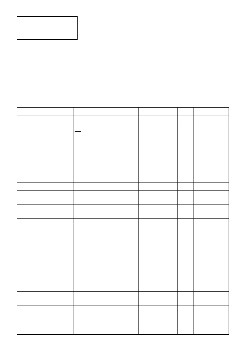
ABSOLUTE MAXIMUM RATING
Input Supply
Voltage Range -0.3 to 20V
Shutdown Input
Voltage Range -0.3 to V
in
Low Battery Output
Voltage Range -0.3 to 20V
ELECTRICAL CHARACTERISTICS
TEST CONDITIONS (Unless otherwise stated) T
Parameter SYMBOL CONDITIONS MIN. TYP. MAX. UNITS
Output voltage V
Output voltage
temperature coefficient
Line regulation
Load regulation
Dropout voltage
(Note3)
Quiescent current I
Quiescent current
at shutdown
Shutdown control input
current
Shutdown control
threshold voltage
Output current in
shutdown mode
(Note4)
Output noise voltage
(Note4)
V
∆T
∆V
∆V
V
I
I
V
I
e
q
qs
ins
Ls
o
o
o
o
in-Vo
ts
n
Vin=5.85V 4.75 4.85 4.95 V
Vin=5.85V
(Note 2, Note 4)
Vin=5.85 to 20V 20 69 mV/V
IL=10 to 300mA
V
=5.85V
in
IL=10mA
I
=100mA
L
I
=300mA
L
Vin=5.85V, IL=0 0.63 1 mA
Vin=5.85V, IL=0,
V
shdn=Vin
V
shdn=Vin
Vin=5.85V
low(on)
high(off) 1.5
Vin=20V
V
=Gnd
o
Vin=5.85V
f=10Hz
to100kHz,
I
=100mA
L
Output Current 300mA
Operating Temperature -40 to 85°C
Storage Temperature -55 to 150°C
Power Dissipation
(T
=25°C) 2W (Note 1)
amb
=25°C,IL=10mA,Cs=10pF,C
amb
100 250 ppm/°C
68 119 mV
6
30
100
11 30
=5.85V 2 10
10
75
200
mV
µA
µA
0.4 V
50 100 nA
190
µV RMS
out
=1µF
Low battery detect
voltage
Low battery flag
output voltage
Low battery flag
leakage current
V
Vo +
in(bld)
V
bl
I
bl
Ibl=100µA,
V
+200mV
in<Vo
Vbl=6V,
V
+400mV
in>Vo
4-72
0.2V
Vo +
0.4V
0.16 0.4 V
0.1 1
V
µA

ZLDO485
NOTES.
1. Maximum power dissipation of the device is calculated assuming the package is mounted on a PCB
measuring 2 inches square.
V
change x
O
2 Output voltage temperature coefficient is calculated as:-
V
x
temperature change
O
3. Dropout voltage is defined as the input to output voltage differential at which the circuit ceases to
regulate. The value is measured when the output voltage has dropped by 100mV from V
= V
at the nominal input V
+ 1V
in
out
4. Guaranteed by design.
FUNCTIONAL DESCRIPTION
The ZLDO is a high performance, ultra low
dropout, low quiescent regulator. Available in
SM8 surface mount packaging, the device is able
to dissipate 2W(note 1) allowing complete design
flexibility with an input span upto 20V and 300mA
output current. The device quiescent is 1mA (t yp)
at 300mA load current. A low battery comparator
signifies impending battery failure, whilst a
shutdown function reduces quiescent current to
a mere 11µA (typ). A precision bandgap
reference gives ± 2.5% output tolerance and
good temperature characteristics over the range
-40 to +85°C. AC performance is enhanced via the
use of a small external capacitor.
PIN DEFINITIONS
Pin 1 LBF - Low Battery Flag. An open collector
NPN output which pulls low on failing input
supply.
Pin 2 SC - Shutdown Control. This high
impedance logic compatible input disables the
regulator when taken high. It includes a diode
wired to Vin and so will pass current if taken more
than 0.5V above Vin.
Pin 3 Vin - Voltage Input. The power supply to
the regulator. The permissible input voltage
range is -0.3 to 20V. An input capacitor is not
mandatory but will be useful in reducing the
coupling of noise from input to output and
minimising the effect of sudden changes in load
current on the input voltage.
Pin 4 N/C - Not Connected. Not internally
connected and so can be left open or wired to an y
pin without affecting the performance of the
Pin 5 Vout - Voltage Output. The output of the
regulator. An output capacitor of 1uF or greater
and having low ESR should be wired in close
proximity to the regulator to ensure stability for
all loads.
Pin 6 D/C - Do Not Connect. This pin is wired to
an internal circuit node of the regulator. No
external connection should be made to this pin.
Pin 7 Gnd - Ground. The ground connection of
the regulator against which the output voltage is
referenced.
Pin 8 Spg - Shaping. The shaping node for
the error amplifier of the regulator. A capacitor
of 10pF wired from this pin to the output pin
(pin 5) gives optimum stability. Improved AC
can be achieved by reducing the value of this
capacitor but stability may be impaired for
some load conditions.
regulator.
1000000
measured
out
4-73
 Loading...