Diodes PDS4150 User Manual

Product Summary
V
(V)
VR(V) IF (A)
150 4.0 0.76 0.01
F MAX
@ +25°C
I
(mA)
R MAX
@ +25°C
Description and Applications
This Schottky Barrier Rectifier has been designed to meet the
stringent requirements of Automotive Applications. It is ideally suited
to use as:
• Polarity Protection Diode
• Re-circulating Diode
• Switching Diode
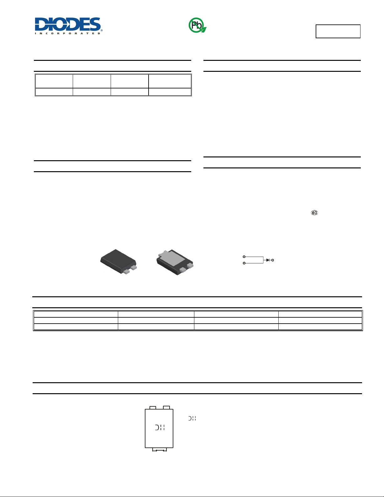
Top View
POWERDI5
Bottom View
Green
PDS4150
4A HIGH VOLTAGE SCHOTTKY BARRIER RECTIFIER
POWERDI
Features and Benefits
• Guard Ring Die Construction for Transient Protection
• Low Forward Voltage Drop
• Very Low Leakage Current
• High Maximum Junction Temperature Capability
• Highly Stable Oxide Passivated Junction
• High Forward Surge Current Capability
• Lead-Free Finish; RoHS Compliant (Notes 1 & 2)
• Halogen and Antimony Free. “Green” Device (Note 3)
• Qualified to AEC-Q101 Standards for High Reliability
• PPAP Capable (Note 4)
Mechanical Data
• Case: POWERDI5
• Case Material: Molded Plastic, “Green” Molding Compound. UL
Flammability Classification Rating 94V-0
• Moisture Sensitivity: Level 1 per J-STD-020
• Terminals: Finish – Matte Tin annealed over Copper leadframe.
Solderable per MIL-STD-202, Method 208
• Polarity: See Diagram
• Weight: 0.096 grams (approximate)
LEFT PIN
RIGHT PIN
Note: Pins Left & Right must
be electrically connected
at the printed circuit board.
BOTTOMSIDE
HEAT SINK
®
Ordering Information (Note 5)
Part Number Compliance Case Packaging
PDS4150-13 Standard POWERDI5 5000/Tape & Reel
PDS4150Q-13 Automotive POWERDI5 5000/Tape & Reel
Notes: 1. EU Directive 2002/95/EC (RoHS) & 2011/65/EU (RoHS 2) compliant. All applicable RoHS exemptions applied.
2. See http://www.diodes.com/quality/lead_free.html for more information about Diodes Incorporated’s definitions of Halogen- and Antimony-free, "Green"
and Lead-free.
3. Halogen- and Antimony-free "Green” products are defined as those which contain <900ppm bromine, <900ppm chlorine (<1500ppm total Br + Cl) and
<1000ppm antimony compounds.
4. Automotive products are AEC-Q101 qualified and are PPAP capable. Automotive, AEC-Q101 and standard products are electrically and thermally
the same, except where specified. For more information, please refer to http://www.diodes.com/quality/product_compliance_definitions/.
5. For packaging details, go to our website at http://www.diodes.com/products/packages.html.
Marking Information
POWERDI is a registered trademark of Diodes Incorporated.
PDS4150
Document number: DS30473 Rev. 14 - 2
S4150
YYWWK
S4150 = Product type marking code
= Manufacturers’ code marking
YYWW = Date code marking
YY = Last two digits of year (ex: 05 for 2014)
WW = Week code (01 - 53)
K = Factory Designator
1 of 4
www.diodes.com
March 2014
© Diodes Incorporated

P
P
OWER
PATIO
NSTAN
T
NEO
U
O
R
R
CUR
R
N
T
Maximum Ratings (@T
= +25°C, unless otherwise specified.)
A
Single phase, half wave, 60Hz, resistive or inductive load.
For capacitance load, derate current by 20%.
Characteristic Symbol Value Unit
Peak Repetitive Reverse Voltage
Working Peak Reverse Voltage
DC Blocking Voltage
RMS Reverse Voltage
Average Rectified Output Current (See also Figure 4)
Non-Repetitive Peak Forward Surge Current
8.3ms Single half sine-wave Superimposed on Rated Load
V
V
V
R(RMS)
I
RRM
RWM
V
R
I
O
FSM
Thermal Characteristics
Characteristic Symbol Typ Max Unit
Thermal Resistance Junction to Soldering Point
Thermal Resistance Junction to Ambient Air (Note 6) TA = +25°C R
Thermal Resistance Junction to Ambient Air (Note 7) TA = +25°C R
Thermal Resistance Junction to Ambient Air (Note 8) TA = +25°C R
Operating and Storage Temperature Range
Electrical Characteristics (@T
= +25°C, unless otherwise specified.)
A
T
PDS4150
R
θJS
θJA
θJA
θJA
, T
J
STG
150 V
106 V
4 A
180 A
⎯
90
60
40
2.0 °C/W
⎯
⎯
⎯
°C/W
°C/W
°C/W
-65 to +175 °C
Characteristic Symbol Min Typ Max Unit Test Condition
Reverse Breakdown Voltage (Note 9)
V
(BR)R
150
⎯
Forward Voltage
V
F
⎯
⎯
⎯
⎯
Reverse Leakage Current (Note 9)
I
R
⎯
⎯
Notes: 6. FR-4 PCB, 2 oz. Copper, minimum recommended pad layout per http://www.diodes.com.
7. Polyimide PCB, 2 oz. Copper, minimum recommended pad layout per http://www.diodes.com.
8. Polyimide PCB, 2 oz. Copper. Cathode pad dimensions 9.4mm x 7.2mm. Anode pad dimensions 2.7mm x 1.6mm.
9. Short duration pulse test used to minimize self-heating effect.
4
(A)
E
3
N (W)
D
100m
WA
2
DISSI
,
D
1
S F
A
10m
1m
⎯ ⎯
0.71
0.57
0.77
0.63
0.3
0.35
0.4
0.76
0.64
0.81
0.70
10
0.8
4.5
V
V
µA
mA
mA
IR = 10µA
= 4A, TS = +25°C
I
F
= 4A, TS = +125°C
I
F
I
= 8A, T
F
= 8A, TS = +125°C
I
F
= +25°C, VR = 150V
T
S
= +125°C, VR = 100V
T
S
T
= +125°C, VR = 150V
S
= +25°C
S
F
2 of 4
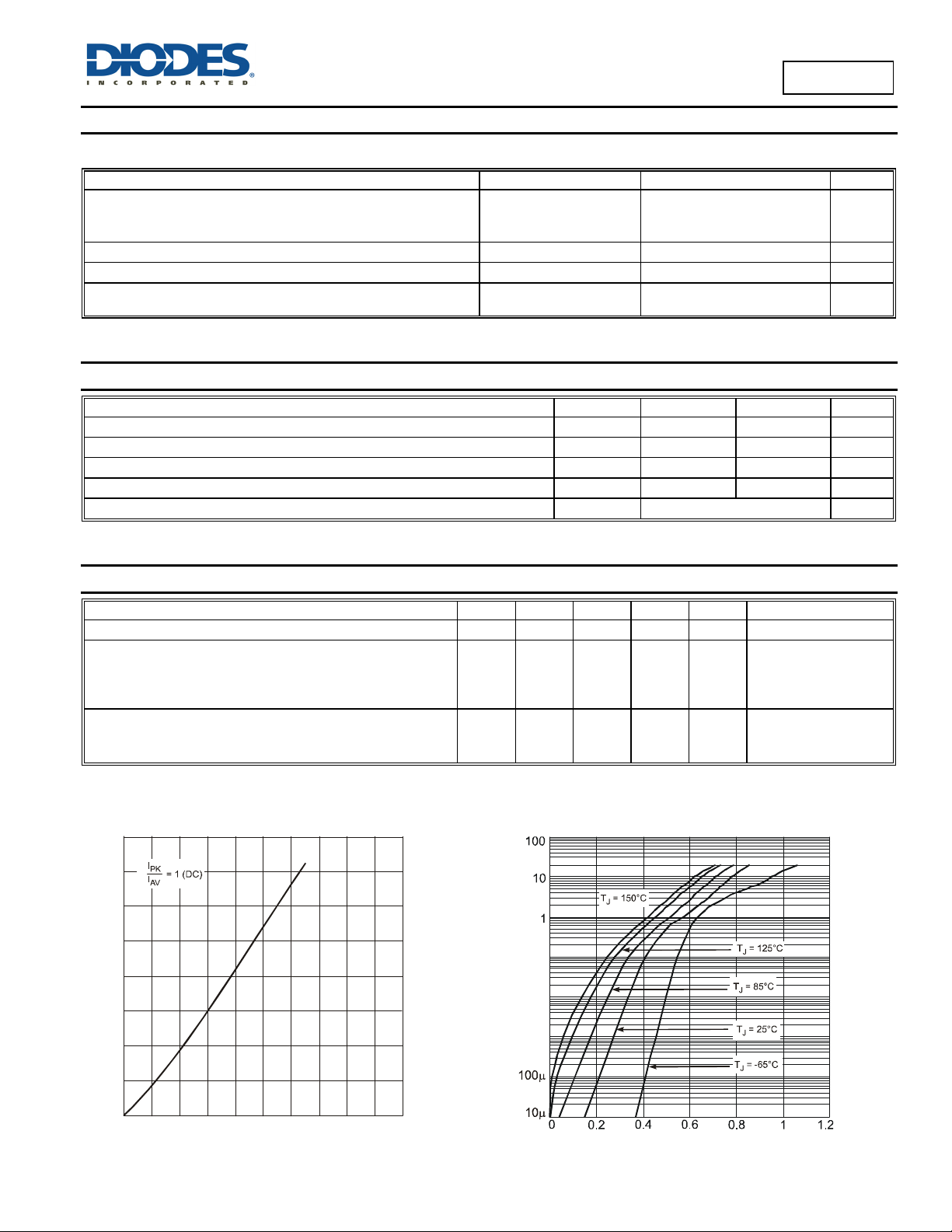
I, I
V , INSTANTANEOUS FORWARD VOLTAGE (V)
F
Fig. 2 Typical Forward Characteristics
March 2014
© Diodes Incorporated
0
0
132
I , AVERAGE RECTIFIED OUTPUT CURRENT (A)
O
4567 8910
Fig. 1 Forward Power Dissipation
POWERDI is a registered trademark of Diodes Incorporated.
PDS4150
Document number: DS30473 Rev. 14 - 2
www.diodes.com
 Loading...