Diodes PDS360 User Manual

Features
• Guard Ring Die Construction for Transient Protection
• Low Power Loss, High Efficiency
• Low Reverse Leakage Current
• For Use in High Frequency Inverters, Free Wheeling, and
Polarity Protection Applications
• High Forward Surge Current Capability
• Lead-Free Finish; RoHS Compliant (Notes 1 & 2)
• Halogen and Antimony Free. “Green” Device (Note 3)
• Qualified to AEC-Q101 Standards for High Reliability
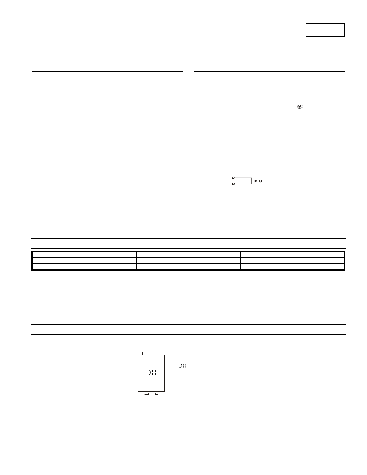
Top View
POWERDI5
Bottom View
Green
3A SCHOTTKY BARRIER RECTIFIER
Mechanical Data
• Case: POWERDI5
• Case Material: Molded Plastic, “Green” Molding Compound. UL
Flammability Classification Rating 94V-0
• Moisture Sensitivity: Level 1 per J-STD-020
• Terminals: Finish – Matte Tin annealed over Copper leadframe.
Solderable per MIL-STD-202, Method 208
• Polarity: See Diagram
• Weight: 0.093 grams (approximate)
LEFT PIN
RIGHT PIN
Note: Pins Left & Right must
be electrically connected
at the printed circuit board.
BOTTOMSIDE
HEAT SINK
PDS360
POWERDI
®
Ordering Information (Note 4)
Part Number Case Packaging
PDS360-13 POWERDI5 5000/Tape & Reel
PDS360-7 POWERDI5 1500/Tape & Reel
Notes: 1. EU Directive 2002/95/EC (RoHS) & 2011/65/EU (RoHS 2) compliant. All applicable RoHS exemptions applied.
2. See http://www.diodes.com for more information about Diodes Incorporated’s definitions of Halogen- and Antimony-free, "Green" and Lead-free.
3. Halogen- and Antimony-free "Green” products are defined as those which contain <900ppm bromine, <900ppm chlorine (<1500ppm total Br + Cl) and
<1000ppm antimony compounds.
4. For packaging details, go to our website at http://www.diodes.com.
Marking Information
POWERDI is a registered trademark of Diodes Incorporated.
PDS360
Document number: DS30479 Rev. 11 - 2
S360
YYWWK
S360 = Product type marking code
= Manufacturers’ code marking
YYWW = Date code marking
YY = Last two digits of year (ex: 05 for 2005)
WW = Week code (01 - 53)
K = Factory Designator
1 of 5
www.diodes.com
October 2012
© Diodes Incorporated

)
θ
θ
θ
θ
(BR)
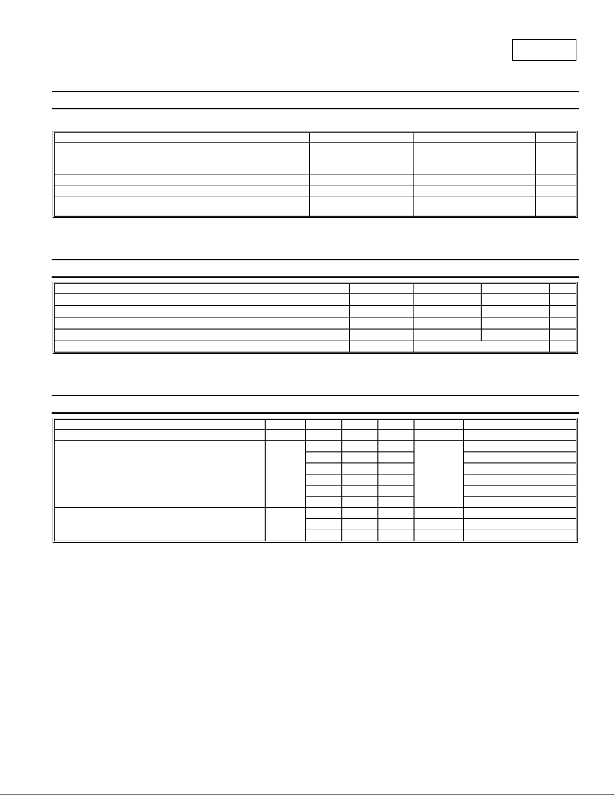
Maximum Ratings (@T
= +25°C, unless otherwise specified.)
A
Single phase, half wave, 60Hz, resistive or inductive load.
For capacitance load, derate current by 20%.
Characteristic Symbol Value Unit
Peak Repetitive Reverse Voltage
Working Peak Reverse Voltage
DC Blocking Voltage
RMS Reverse Voltage
Average Rectified Output Current (See also Figure 4)
Non-Repetitive Peak Forward Surge Current
8.3ms Single half sine-wave superimposed on rated load
Thermal Characteristics
Characteristic Symbol Typ Max Unit
Thermal Resistance Junction to Soldering Point
Thermal Resistance Junction to Ambient Air (Note 5) TA = +25°C
Thermal Resistance Junction to Ambient Air (Note 6) TA = +25°C
Thermal Resistance Junction to Ambient Air (Note 7) TA = +25°C
Operating and Storage Temperature Range
V
V
V
RRM
RWM
V
R
R(RMS
I
O
I
FSM
PDS360
R
JS
R
JA
R
JA
R
JA
, T
T
J
STG
60 V
42 V
3 A
100 A
⎯
95
70
50
3.0
⎯
⎯
⎯
-65 to +150
°C/W
°C/W
°C/W
°C/W
°C
Electrical Characteristics (@T
= +25°C, unless otherwise specified.)
A
Characteristic Symbol Min Typ Max Unit Test Condition
Reverse Breakdown Voltage (Note 8)
Forward Voltage
Reverse Leakage Current (Note 8)
Notes: 5. FR-4 PCB, 2 oz. Copper, minimum recommended pad layout per http://www.diodes.com.
6. Polymide PCB, 2 oz. Copper, minimum recommended pad layout per http://www.diodes.com.
7. Polymide PCB, 2 oz. Copper. Cathode pad dimensions 9.4 mm x 7.4 mm. Anode pad dimensions 2.7 mm x 1.6 mm.
8. Short duration pulse test used to minimize self-heating effect.
V
V
F
I
R
R
60
⎯
⎯
⎯
⎯
⎯
⎯
⎯ ⎯
0.57 0.62
0.53 0.60
0.51 0.57
0.70 0.76
0.62 0.70
0.60 0.66
⎯
⎯ ⎯
⎯
1.5 15 mA
3 150
10 mA
V
V
μA
IR = 0.2mA
I
= 3A, TJ = +25°C
F
= 3A, TJ = +100°C
I
F
= 3A, TJ = +125°C
I
F
= 6A, TJ = +25°C
I
F
= 6A, TJ = +100°C
I
F
= 6A, TJ = +125°C
I
F
T
= +25°C, VR = 60V
J
= +100°C, VR = 60V
T
J
= +125°C, VR = 60V
T
J
POWERDI is a registered trademark of Diodes Incorporated.
PDS360
Document number: DS30479 Rev. 11 - 2
2 of 5
www.diodes.com
October 2012
© Diodes Incorporated
 Loading...