Diodes PD3S130L User Manual

Please click here to visit our online spice models database.
Features
• Ultra-Small Surface Mount Package
• Guard Ring Die Construction for Transient Protection
• High Surge Capability
• Lead Free Finish, RoHS Compliant (Note 1)
• "Green" Molding Compound (No Br, Sb)
• Qualified to AEC-Q101 Standards for High Reliability
Maximum Ratings @T
Single phase, half wave, 60Hz, resistive or inductive load.
For capacitance load, derate current by 20%.
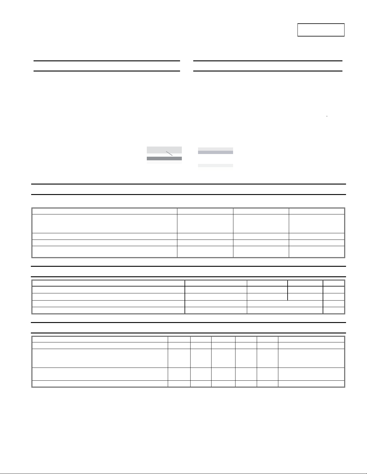
Characteristic Symbol Value Unit
Peak Repetitive Reverse Voltage
Working Peak Reverse Voltage
DC Blocking Voltage
RMS Reverse Voltage
Average Forward Current (See also figure 4)
Non-Repetitive Peak Forward Surge Current 8.3ms
Single Half Sine-Wave Superimposed on Rated Load
= 25°C unless otherwise specified
A
Top View
PD3S130L
1.0A SURFACE MOUNT SCHOTTKY BARRIER RECTIFIER
PowerDI
®
323
Mechanical Data
• Case: PowerDI®323
• Case Material: Molded Plastic, “Green” Molding Compound.
UL Flammability Classification Rating 94V-0
• Moisture Sensitivity: Level 1 per J-STD-020D
• Polarity: Cathode Band
• Terminals: Finish - Matte Tin annealed over Copper
leadframe. Solderable per MIL-STD-202, Method 208
• Marking Information: See Page 3
• Ordering Information: See Page 3
• Weight: 0.006 grams (approximate)
Bottom View
V
V
V
R(RMS)
I
F(AV)
I
RRM
RWM
VR
FSM
30 V
21 V
1.0 A
22 A
Thermal Characteristics
Characteristic Symbol Typ Max Unit
Thermal Resistance Junction to Soldering Point
Thermal Resistance Junction to Ambient Air (Note 2)
Operating Temperature Range
Storage Temperature Range
Electrical Characteristics @T
Characteristic Symbol Min Typ Max Unit Test Condition
Reverse Breakdown Voltage (Note 3)
Forward Voltage
Leakage Current (Note 3)
Total Capacitance
Notes: 1. EU Directive 2002/95/EC (RoHS). All applicable RoHS exemptions applied, see EU Directive 2002/95/EC Annex Notes.
PowerDI is a registered trademark of Diodes Incorporated.
PD3S130L
Document number: DS30671 Rev. 9 - 2
2. FR-4 PCB, 2 oz. Copper, minimum recommended pad layout per http://www.diodes.com/datasheets/ap02001.pdf. T
3. Short duration pulse test used to minimize self-heating effect.
= 25°C unless otherwise specified
A
1 of 3
30
⎯
⎯
⎯
⎯
⎯
V
(BR)R
VF
IR
CT ⎯
www.diodes.com
R
JS
θ
R
JA
θ
TJ
T
STG
⎯ ⎯
0.25
0.33
0.39
40
0.37
40
0.33
0.37
0.42
250
1.5
⎯
⎯
177
-65 to +125
-65 to +150
V
IR = 1.5mA
IF = 0.1A
V
IF = 0.7A
IF = 1.0A
VR = 5V, TA = 25°C
μA
mA
VR = 30V, TA = 25°C
pF
VR = 10V, f = 1.0MHz
= 25°C.
A
6.0
⎯
June 2008
© Diodes Incorporated
°C/W
°C/W
°C
°C

P, P
OWER
P
TIO
NSTAN
TANEO
US F
O
R
RD CUR
REN
T
C, TOT
CAPACITAN
C
F
NSTAN
TANEO
US R
R
CUR
REN
T
T
R
T
T T
PERATUR
C
R
G
FORWAR
C
URREN
T
PD3S130L
0.9
0.8
0.7
N (W)
0.6
A
0.5
DISSI
0.4
10,000
(mA)
1,000
100
WA
10
0.3
D
0.2
1
0.1
0.1
F
I, I
0.200.4
V , INSTANT ANEOU S FORWARD VOL TAGE (V)
F
0.6 0.8 1.0
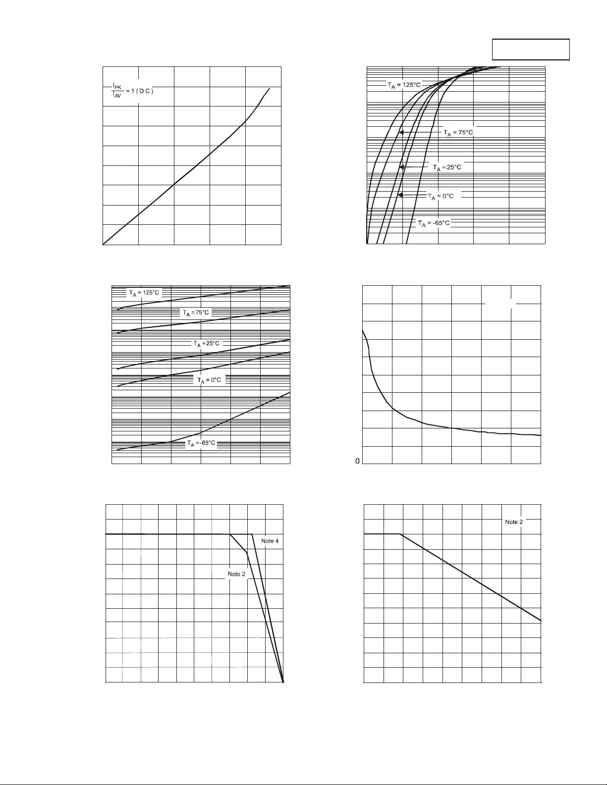
Fig. 2 Typical Forward Ch ar acteristics
200
f = 1MHz
)
E (p
180
160
140
120
100,000
(uA)
10,000
1,000
100
SE
0
0
0.5 1.0 1.5
I , AVERAGE FORWARD CURRENT (A)
F(AV)
Fig. 1 Forward Power Dissipation
2.0 2.5
AL
100
80
EVE
10
1
60
I, I
R
0.001
(A)
0.1
0.01
0
V , INSTANTANEOUS REVERSE VOLTAGE (V)
R
10 15 20
5
Fig. 3 Typical Reverse Characteristics
1.2
1.0
0.8
25
30
T
40
20
0 5 10 15 20 25 30
V , DC REVERSE VOLTAGE (V)
R
Fig. 4 Total Capacitance vs. Reverse Voltage
150
)
E (°
125
100
D
EM
0.6
E
0.4
A
75
50
ED AMBIEN
0.2
F(AV)
I, AVE
0
0255075
T , AMBIENT TEMPERATURE (°C)
A
Fig. 5 Forward Current Derating Curve
Notes: 4. Polymide PCB, 2 oz. Copper, minimum recommended pad layout per http://www.diodes.com/datasheets/ap02001.pdf.
100
125
A
25
, DE
A
0
0
Fig. 6 Oper at ing Tempe r ature Derati ng
10 20 30
V , DC REVERSE VOL TAGE (V)
R
owerDI is a registered trademark of Diodes Incorporated.
P
PD3S130L
Document number: DS30671 Rev. 9 - 2
2 of 3
www.diodes.com
June 2008
© Diodes Incorporated
 Loading...