Diodes PD3S120L User Manual

Please click here to visit our online spice models database.
Features
• Guard Ring Die Construction for Transient Protection
• High Surge Capability
• Lead Free Finish, RoHS Compliant (Note 1)
• "Green" Molding Compound (No Br, Sb)
• Ultra-Small Surface Mount Package
• Qualified to AEC-Q101 Standards for High Reliability
Maximum Ratings @T
Single phase, half wave, 60Hz, resistive or inductive load.
For capacitance load, derate current by 20%.
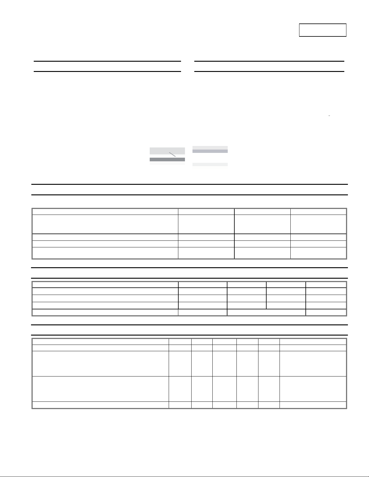
Characteristic Symbol Value Unit
Peak Repetitive Reverse Voltage
Working Peak Reverse Voltage
DC Blocking Voltage
RMS Reverse Voltage
Average Forward Current (See also figure 4)
Non-Repetitive Peak Forward Surge Current 8.3ms
single half sine-wave superimposed on rated load
= 25°C unless otherwise specified
A
1.0A SURFACE MOUNT SCHOTTKY BARRIER RECTIFIER
Mechanical Data
• Case: PowerDI®323
• Case Material: Molded Plastic, “Green” Molding Compound.
UL Flammability Classification Rating 94V-0
• Moisture Sensitivity: Level 1 per J-STD-020D
• Polarity: Cathode Band
• Terminals: Finish - Matte Tin annealed over Copper
leadframe. Solderable per MIL-STD-202, Method 208
• Marking Information: See Page 3
• Ordering Information: See Page 3
• Weight: 0.006 grams (approximate)
Top View Bottom View
V
RRM
V
RWM
VR
V
R(RMS)
I
F(AV)
I
FSM
PD3S120L
PowerDI
20 V
14 V
1.0 A
33 A
®
323
Thermal Characteristics
Characteristic Symbol Typ Max Unit
Thermal Resistance Junction to Soldering Point
Thermal Resistance Junction to Ambient Air (Note 2)
Thermal Resistance Junction to Ambient Air (Note 3)
Operating and Storage Temperature Range
Electrical Characteristics @T
Characteristic Symbol Min Typ Max Unit Test Condition
Reverse Breakdown Voltage (Note 4)
Forward Voltage
Leakage Current (Note 4)
Total Capacitance
Notes: 1. EU Directive 2002/95/EC (RoHS). All applicable RoHS exemptions applied, see EU Directive 2002/95/EC Annex Notes.
PowerDI is a registered trademark of Diodes Incorporated.
PD3S120L
Document number: DS30793 Rev. 4 - 2
2. FR-4 PCB, 2 oz. Copper, minimum recommended pad layout per http://www.diodes.com/datasheets/ap02001.pdf.
3. Polymide PCB, 2 oz. Copper, minimum recommended pad layout per http://www.diodes.com/datasheets/ap02001.pdf.
4. Short duration pulse test to minimize self-heating effect.
= 25°C unless otherwise specified
A
R
R
R
TJ, T
1 of 3
20
⎯
⎯
⎯
⎯
⎯
V
(BR)R
VF
IR
CT ⎯
www.diodes.com
θ
θ
θ
JS
JA
JA
STG
⎯ ⎯
0.27
0.34
0.36
0.27
10
13
30
11
46
⎯
170
144
0.31
0.38
0.42
0.30
50
60
160
30
⎯
-65 to +125
V
V
μA
μA
μA
mA
pF
6
⎯
⎯
IR = 100μA
IF = 0.1A, TA = 25ºC
IF = 0.7A, TA = 25ºC
IF = 1.0A, TA = 25ºC
IF = 1.0A, TA = 125ºC
VR = 5V, TA = 25°C
VR = 10V, TA = 25°C
VR = 20V, TA = 25°C
VR = 20V, TA = 125°C
VR = 10V, f = 1.0MHz
°C/W
°C/W
°C/W
°C
© Diodes Incorporated
June 2008

P, P
OWER
PAT
O
R
G
FOR
R
CUR
RENT
T
RAT
T
TEMPERATUR
C
PD3S120L
0.8
0.7
0.6
N (W)
I
0.5
0.4
DISSI
I
PK
____
I
AV
= 1(DC)
T = 125°C
J
T = 85°C
J
T = 25°C
J
T = -65°C
J
0.3
0.2
D
0.1
0
0 0.5 1 1.5 2 2.5
I , AVERAGE FORWARD CURRENT (A)
F(AV)
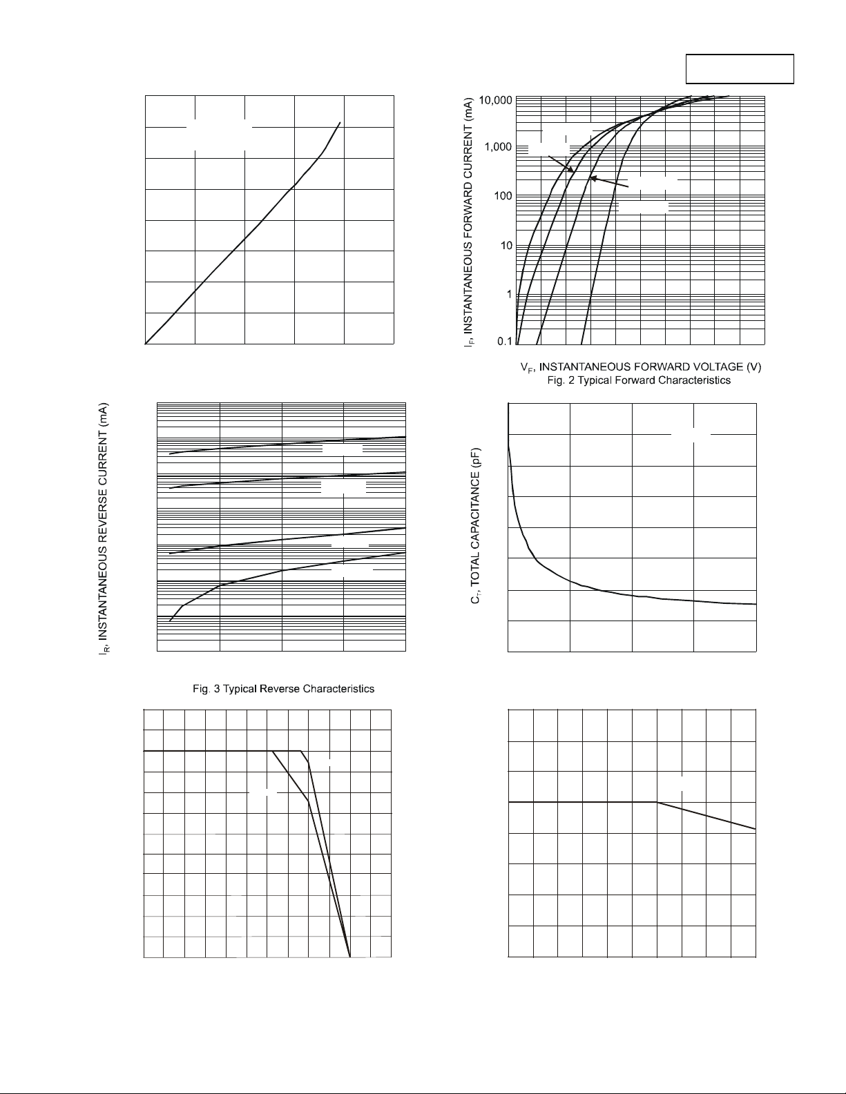
Fig. 1 Forward Power Dissipation
100
10
1
T = 125°C
J
T = 85°C
J
0 0.2 0.4 0.6 0.8 1
200
f = 1.0MHz
150
0.1
100
T = 25°C
0.01
J
T = -65°C
0.001
J
50
0.0001
0.00001
0 5 10 15 20
V , INSTANTANEOUS REVERSE VOLTAGE (V)
R
1.2
(A)
D
WA
1.0
0.8
0.6
Note 2
Note 3
0
0 5 10 15 20
V , DC REVERSE VOL TAGE (V)
R
Fig. 4 Total Capacitance vs. Reverse Voltage
200
)
E (°
150
Note 2
100
E
0.4
A
50
ED AMBIEN
0.2
F(AV)
I, AVE
0
025
50 75
T , AMBIENT TEMPERATURE (°C)
A
100 125
Fig. 5 Forward Current Derating Curve
owerDI is a registered trademark of Diodes Incorporated.
P
PD3S120L
Document number: DS30793 Rev. 4 - 2
150
2 of 3
www.diodes.com
, DE
A
0
0
V , DC REVERSE VOLTAGE (V)
R
10
Fig. 6 Operating Temperature Derating
20
June 2008
© Diodes Incorporated
 Loading...