

Page 1
Features
• 600W Peak Pulse Power Dissipation
• Voltage Range 6.8V - 400V
• Constructed with Glass Passivated Die
• Uni- and Bidirectional Versions Available
• Excellent Clamping Capability
• Fast Response Time
• Lead Free Finish, RoHS Compliant (Note 1)
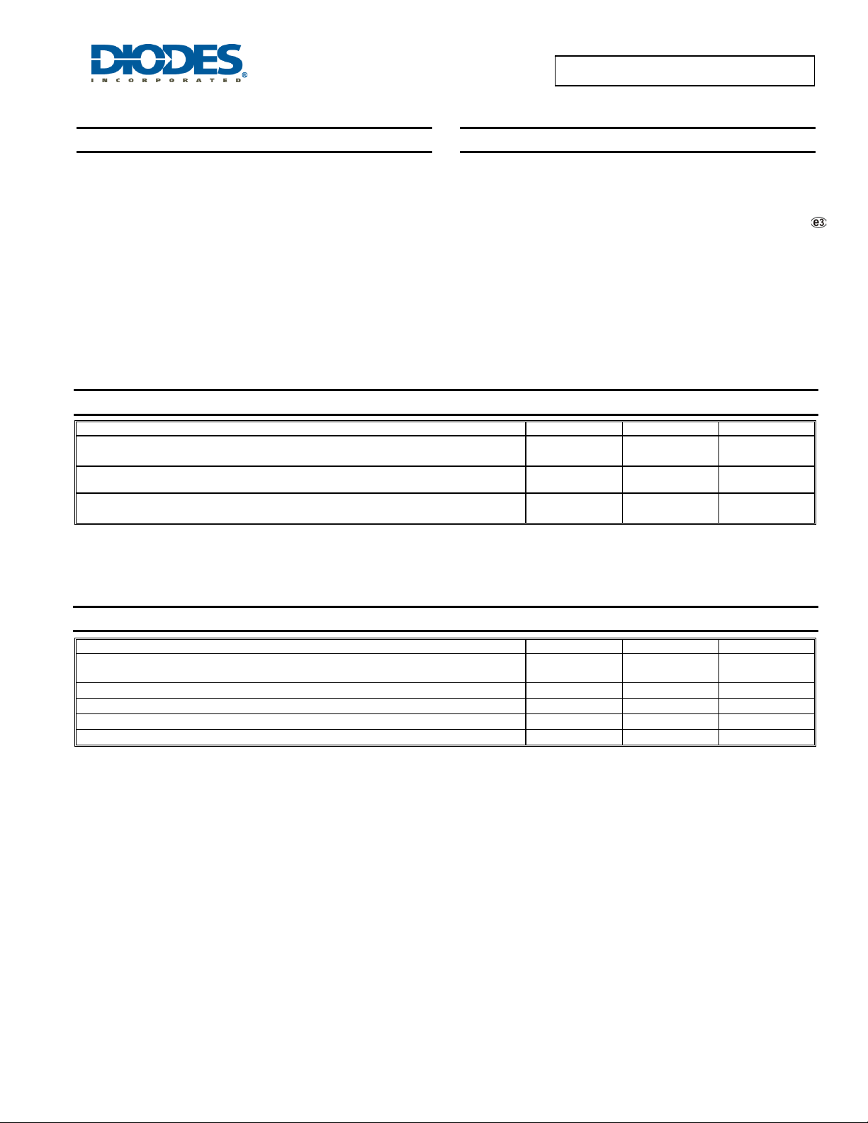
Maximum Ratings @T
Peak Power Dissipation, tp = 1.0 ms
(Non repetitive current pulse, derated above T
Peak Forward Surge Current, 8.3ms Single Half Sine Wave, Superimposed on Rated
Load Duty Cycle = 4 pulses per minute maximum
Forward Voltage @ IF = 35A VBR ≤ 200V
300µs Square Wave Pulse, Unidirectional Only V
= 25°C unless otherwise specified
A
Characteristic Symbol Value Unit
= 25°C)
A
Mechanical Data
• Case: DO-15
• Case Material: Molded Plastic. UL Flammability Classification
Rating 94V-0
• Moisture Sensitivity: Level 1 per J-STD-020
• Leads: Plated Leads, Solderable per MIL-STD-202, Method 208
• Marking: Unidirectional - Type Number and Cathode Band
• Marking: Bidirectional - Type Number Only
• Ordering Information: See Page 4
• Weight: 0.4 grams (approximate)
> 200V
BR
P6KE6V8(C)A - P6KE400(C)A
600W TRANSIENT VOLTAGE SUPPRESSOR
P
I
FSM
V
pk
F
600 W
100 A
3.5
5.0
V
Thermal Characteristics
Characteristic Symbol Value Unit
Steady State Power Dissipation at TL = 75°C
Lead Lengths 9.5 mm (Mounted on Copper Land Area of 40mm)
Typical Thermal Resistance, Junction to Case
Typical Thermal Resistance, Junction to Lead
Typical Thermal Resistance, Junction to Ambient
Operating and Storage Temperature Range
Notes: 1. EU Directive 2002/95/EC (RoHS). All applicable RoHS exemptions applied, see EU Directive 2002/95/EC Annex Notes.
P6KE6V8(C)A - P6KE400(C)A
Document number: DS21502 Rev. 18 - 2
1 of 5
www.diodes.com
P
D
R
θJC
R
θJL
R
θJA
T
, T
J
STG
-55 to +175 °C
5.0 W
20 °C/W
15 °C/W
75 °C/W
March 2010
© Diodes Incorporated
Page 2
P6KE6V8(C)A - P6KE400(C)A
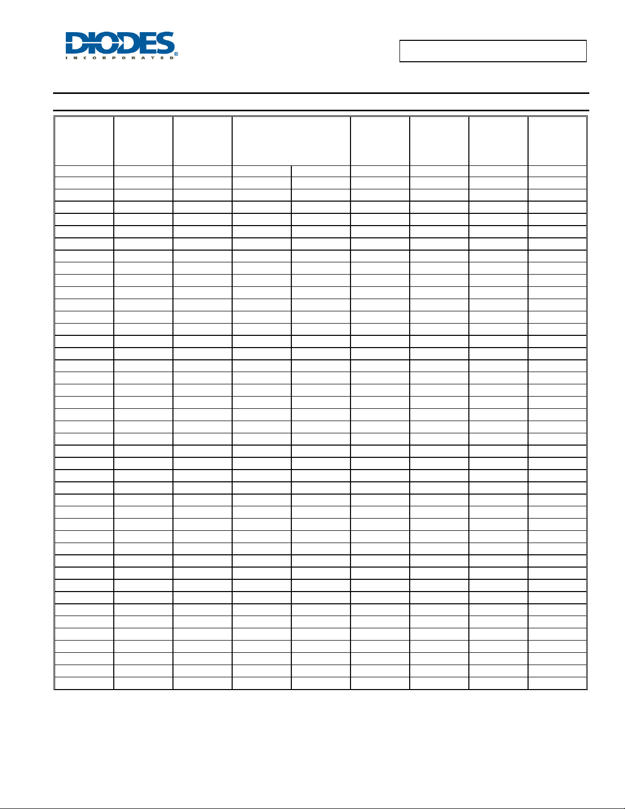
Electrical Characteristics @T
Type
Number
(Note 2)
Type
Number
(Note 2)
(UNI) (BI)
Reverse
Standoff
Voltage
V
RWM
= 25°C unless otherwise specified
A
Breakdown Voltage
V
BR @ IT
(V)
Min (V) Max (V)
Test
Current
Max
Reverse
Leakage
(Note 3)
@ V
R
Max
Clamping
Voltage
@ I
pp
Pulse Current
IT(mA) IR (μA) VC (V) I
Max Peak
(A)
PP
P6KE6V8A P6KE6V8CA 5.80 6.45 7.14 10 1000 10.5 57.0
P6KE7V5A P6KE7V5CA 6.40 7.13 7.88 10 500 11.3 53.0
P6KE8V2A P6KE8V2CA 7.02 7.79 8.61 10 200 12.1 50.0
P6KE9V1A P6KE9V1CA 7.78 8.65 9.55 1.0 50 13.4 45.0
P6KE10A P6KE10CA 8.55 9.50 10.50 1.0 10 14.5 41.0
P6KE11A P6KE11CA 9.40 10.50 11.60 1.0 5.0 15.6 38.0
P6KE12A P6KE12CA 10.20 11.40 12.60 1.0 5.0 16.7 36.0
P6KE13A P6KE13CA 11.10 12.40 13.70 1.0 5.0 18.2 33.0
P6KE15A P6KE15CA 12.80 14.30 15.80 1.0 5.0 21.2 28.0
P6KE16A P6KE16CA 13.60 15.20 16.80 1.0 5.0 22.5 27.0
P6KE18A P6KE18CA 15.30 17.10 18.90 1.0 5.0 25.2 24.0
P6KE20A P6KE20CA 17.10 19.00 21.00 1.0 5.0 27.7 22.0
P6KE22A P6KE22CA 18.80 20.90 23.10 1.0 5.0 30.6 20.0
P6KE24A P6KE24CA 20.50 22.80 25.20 1.0 5.0 33.2 18.0
P6KE27A P6KE27CA 23.10 25.70 28.40 1.0 5.0 37.5 16.0
P6KE30A P6KE30CA 25.60 28.50 31.50 1.0 5.0 41.4 14.40
P6KE33A P6KE33CA 28.20 31.40 34.70 1.0 5.0 45.7 13.20
P6KE36A P6KE36CA 30.80 34.20 37.80 1.0 5.0 49.9 12.00
P6KE39A P6KE39CA 33.30 37.10 41.00 1.0 5.0 53.9 11.20
P6KE43A P6KE43CA 36.80 40.90 45.20 1.0 5.0 59.3 10.10
P6KE47A P6KE47CA 40.20 44.70 49.40 1.0 5.0 64.8 9.30
P6KE51A P6KE51CA 43.60 48.50 53.60 1.0 5.0 70.1 8.60
P6KE56A P6KE56CA 47.80 53.20 58.80 1.0 5.0 77.0 7.80
P6KE62A P6KE62CA 53.00 58.90 65.10 1.0 5.0 85.0 7.10
P6KE68A P6KE68CA 58.10 64.60 71.40 1.0 5.0 92.0 6.50
P6KE75A P6KE75CA 64.10 71.30 78.80 1.0 5.0 103.0 5.80
P6KE82A P6KE82CA 70.10 77.90 86.10 1.0 5.0 113.0 5.30
P6KE91A P6KE91CA 77.80 86.50 95.50 1.0 5.0 125.0 4.80
P6KE100A P6KE100CA 85.50 95.00 105.00 1.0 5.0 137.0 4.40
P6KE110A P6KE110CA 94.00 105.00 116.00 1.0 5.0 152.0 4.00
P6KE120A P6KE120CA 102.00 114.00 126.00 1.0 5.0 165.0 3.60
P6KE130A P6KE130CA 111.00 124.00 137.00 1.0 5.0 179.0 3.30
P6KE150A P6KE150CA 128.00 143.00 158.00 1.0 5.0 207.0 2.90
P6KE160A P6KE160CA 136.00 152.00 168.00 1.0 5.0 219.0 2.70
P6KE170A P6KE170CA 145.00 162.00 179.00 1.0 5.0 234.0 2.60
P6KE180A P6KE180CA 154.00 171.00 189.00 1.0 5.0 246.0 2.40
P6KE200A P6KE200CA 171.00 190.00 210.00 1.0 5.0 274.0 2.20
P6KE220A P6KE220CA 185.00 209.00 231.00 1.0 5.0 328.0 1.83
P6KE250A P6KE250CA 214.00 237.00 263.00 1.0 5.0 344.0 1.75
P6KE300A P6KE300CA 256.00 285.00 315.00 1.0 5.0 414.0 1.45
P6KE350A P6KE350CA 300.00 332.00 368.00 1.0 5.0 482.0 1.25
P6KE400A P6KE400CA 342.00 380.00 420.00 1.0 5.0 548.0 1.10
Notes: 2. Suffix ‘C’ denotes bidirectional device.
3. For bidirectional devices having V
of 10 volts and under, the IR limit is doubled.
R
P6KE6V8(C)A - P6KE400(C)A
Document number: DS21502 Rev. 18 - 2
2 of 5
www.diodes.com
March 2010
© Diodes Incorporated
Page 3

C, C
P
C
T
C
P
P
U
RATIN
G
P
T
Y
T
T
P
O
R
PAT
O
N
P
FOR
R
U
R
GE CUR
REN
T
Ppp
I , PEAK PULSE CURRENT (% )
100
t, TIME (ms)
Fig. 1 Pulse Waveform
P6KE6V8(C)A - P6KE400(C)A
10,000
Measured at
Zero Bias
1,000
E (pF)
AN
I
A
A
100
T
Measured at
Stand-off Voltage
10
1 10 100 1,000
V , REVERSE STANDOFF VOLTAGE (V)
RWM
Fig. 2 Typical Total Capacitance
100
T = 25°C
j
f = 1.0 MHz
V = 50mV p-p
sig
Impulse
75
10
50
LSE DE
1.0
EAK
25
P
P , PEAK PULSE POWER (kW)
0.1
T = 25°C
C
0.1 1.0
10 100
1,000 10,000
(% PEAK POWER OR CURRENT)
10 X 1000 Waveform
as defined by REA
0
0 25 50 75 100 125 150 175 200
T , AMBIENT TEMPERATURE (°C)
A
Fig. 4 Pulse Derating Curve
5.0
(W)
I
Single phase
half-wave 60Hz
resistive or
inductive load
1,000
(A)
3.75
DISSI
WE
E
A
S
2.5
100
D S
WA
10
1.25
EAD
, S
d
0
25 50 75 100 125 150 175
0
T , LEAD TEMPERATURE (°C)
L
Fig. 5, Steady State Power Derating
200
EAK
FSM
I,
0
110100200
NUMBER OF CYCLES AT 60Hz
Fig. 6 Peak Forward Surge Current
vs. Number of Cycles at 60Hz
P6KE6V8(C)A - P6KE400(C)A
Document number: DS21502 Rev. 18 - 2
3 of 5
www.diodes.com
March 2010
© Diodes Incorporated
Page 4

P6KE6V8(C)A - P6KE400(C)A
Ordering Information (Note 4)
Part Number Case Packaging
(Type Number)-B* DO-15 500/Bulk
(Type Number)-T* DO-15 4K/Tape & Reel, 13-inch
* Add "-B" or "-T" to the appropriate type number in Table 1 for Bulk or Tape & Reel, respectively. Example: 6.40V VRWM = P6KE7V5A-B for Bulk, P6KE7V5A-T for
Tape & Reel.
Notes: 4. For packaging details, go to our website at http://www.diodes.com/datasheets/ap02008.pdf.
Package Outline Dimensions
Dim Min Max
A 25.40
B 5.50 7.62
C 0.686 0.889
D 2.60 3.60
All Dimensions in mm
DO-15
⎯
P6KE6V8(C)A - P6KE400(C)A
Document number: DS21502 Rev. 18 - 2
4 of 5
www.diodes.com
March 2010
© Diodes Incorporated
Page 5

IMPORTANT NOTICE
DIODES INCORPORATED MAKES NO WARRANTY OF ANY KIND, EXPRESS OR IMPLIED, WITH REGARDS TO THIS DOCUMENT,
INCLUDING, BUT NOT LIMITED TO, THE IMPLIED WARRANTIES OF MERCHANTABILITY AND FITNESS FOR A PARTICULAR PURPOSE
(AND THEIR EQUIVALENTS UNDER THE LAWS OF ANY JURISDICTION).
Diodes Incorporated and its subsidiaries reserve the right to make modifications, enhancements, improvements, corrections or other changes
without further notice to this document and any product described herein. Diodes Incorporated does not assume any liability arising out of the
application or use of this document or any product described herein; neither does Diodes Incorporated convey any license under its patent or
trademark rights, nor the rights of others. Any Customer or user of this document or products described herein in such applications shall assume
all risks of such use and will agree to hold Diodes Incorporated and all the companies whose products are represented on Diodes Incorporated
website, harmless against all damages.
Diodes Incorporated does not warrant or accept any liability whatsoever in respect of any products purchased through unauthorized sales channel.
Should Customers purchase or use Diodes Incorporated products for any unintended or unauthorize d application, Customers shall indemnify and
hold Diodes Incorporated and its representatives harmless against all claims, damages, expenses, and attorney fees arising out of, directly or
indirectly, any claim of personal injury or death associated with such unintended or unauthorized application.
Products described herein may be covered by one or more United States, international or foreign patents pending. Product names and markings
noted herein may also be covered by one or more United States, international or foreign trademarks.
LIFE SUPPORT
Diodes Incorporated products are specifically not authorized for use as critical components in life support devices or systems without the express
written approval of the Chief Executive Officer of Diodes Incorporated. As used herein:
A. Life support devices or systems are devices or systems which:
1. are intended to implant into the body, or
2. support or sustain life and whose failure to perform when properly used in accordance with instructions for use provided in the
labeling can be reasonably expected to result in significant injury to the user.
B. A critical component is any component in a life support device or system whose failure to perform can be reasonably expected to cause the
failure of the life support device or to affect its safety or effectiveness.
Customers represent that they have all necessary expertise in the safety and regulatory ramifications of their life support devices or systems, and
acknowledge and agree that they are solely responsible for all legal, regulatory and safety-related requirements concerning their products and any
use of Diodes Incorporated products in such safety-critical, life support devices or systems, notwithstanding any devices- or systems-related
information or support that may be provided by Diodes Incorporated. Further, Customers must fully indemnify Diodes Incorporated and its
representatives against any damages arising out of the use of Diodes Incorporated products in such safety-critical, life support devices or systems.
Copyright © 2009, Diodes Incorporated
www.diodes.com
P6KE6V8(C)A - P6KE400(C)A
P6KE6V8(C)A - P6KE400(C)A
Document number: DS21502 Rev. 18 - 2
5 of 5
www.diodes.com
March 2010
© Diodes Incorporated
 Loading...