Page 1
Description
These devices are precision timing circuits capable of
producing accurate time delays or oscillation. In the timedelay or monostable mode of operation, the timed interval is
controlled by a single external resistor and capacitor network.
In the astable mode of operation, the frequency and duty
cycle can be controlled independently with two external
resistors and a single external capacitor.
The threshold and trigger levels normally are t wo-thirds and
one-third, respectively, of V
by use of the control-voltage terminal. When the trigger input
falls below the trigger level, the flip-flop is set, and the out put
goes high. If the trigger input is above the trigger level and
the threshold input is above the threshold level, the flip-flop is
reset and the output is low. The reset (RESET) input can
override all other inputs and can be used to initiate a new
timing cycle. When RESET goes low, the flip-flop is reset,
and the output goes low. When the output is low, a lowimpedance path is provided between discharge (DISCH) and
NEW PRODUCT
ground.
The output circuit is capable of sinking or sourcing current up
to 200mA. Operation is specified for supplies of 5V to 15V.
With a 5-V supply, output levels are compatible with TTL
inputs.
Features
. These levels can be altered
CC
NE555/SA555/NA555
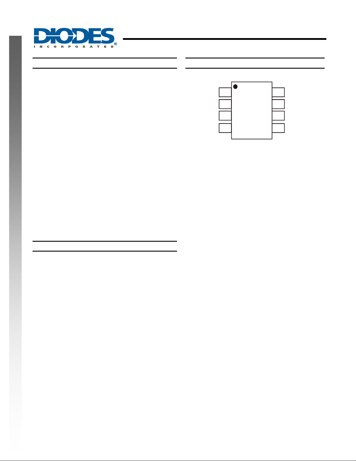
Pin Assignments
(Top View)
GND
TRIG
OUT
RESET
PRECISION TIMERS
SO-8
V
CC
DISCH
THRES
CONT
• Timing from microseconds to hours
• Astable or monostable operation
• Adjustable duty cycle
• TTL compatible output can source or sink up to 200mA
• “Green” Molding Compound (No Br, Sb)
• Lead Free Finish/ RoHS Compliant (Note 1)
Notes: 1. EU Directive 2002/95/EC (RoHS). All applicable RoHS exemptions applied. Please visit our website at
http://www.diodes.com/products/lead_free.html.
NE555/SA555/NA555
Document number: DS35112 Rev. 4 - 2
1 of 14
www.diodes.com
February 2012
© Diodes Incorporated
Page 2
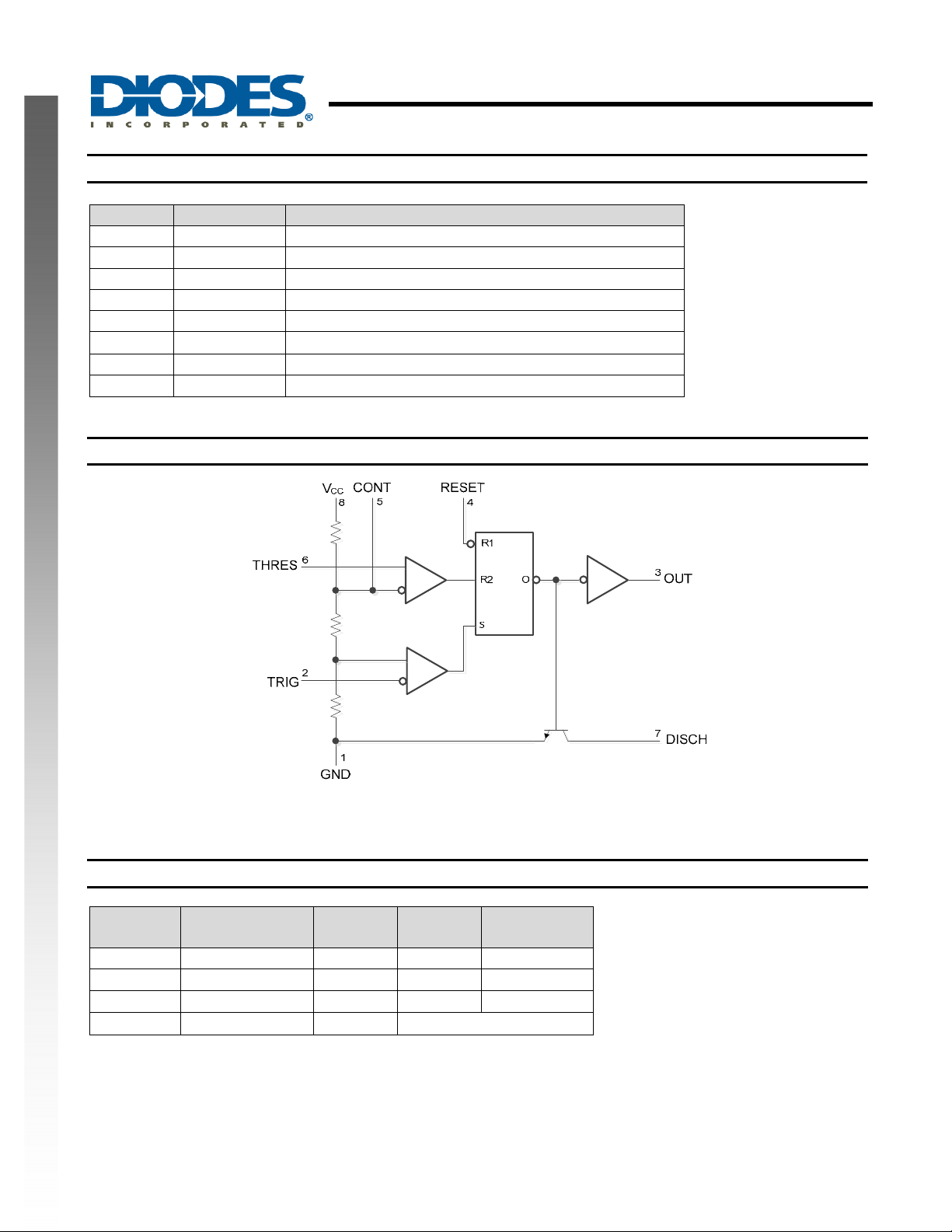
Pin Descriptions
Pin Name Pin Number Description
GND 1 Ground
TRIG 2
OUT 3 Timer output
RESET 4 Reset active low
CONT 5 External adjustment of internal threshold and trigger voltages
THRES 6
DISCH 7 Low impedance discharge path
VCC
Functional Block Diagram
NEW PRODUCT
Functional Table
Pin Name
GND Irrelevant Irrelevant Low On
TRIG
OUT
RESET
Nominal Trigger
Voltage
<1/3V
<1/3V
<1/3V
Trigger set 1/3V
Threshold set to 2/3 V
8 Chip supply voltage
CC
RESET can override TRIG, which can override THRESH
Threshold
Voltage
CC
<2/3VCC
CC
<2/3VCC
CC
Irrelevant High Off
NE555/SA555/NA555
CC
Output
Low On
As previously established
Discharge
Switch
PRECISION TIMERS
NE555/SA555/NA555
Document number: DS35112 Rev. 4 - 2
2 of 14
www.diodes.com
February 2012
© Diodes Incorporated
Page 3
NE555/SA555/NA555
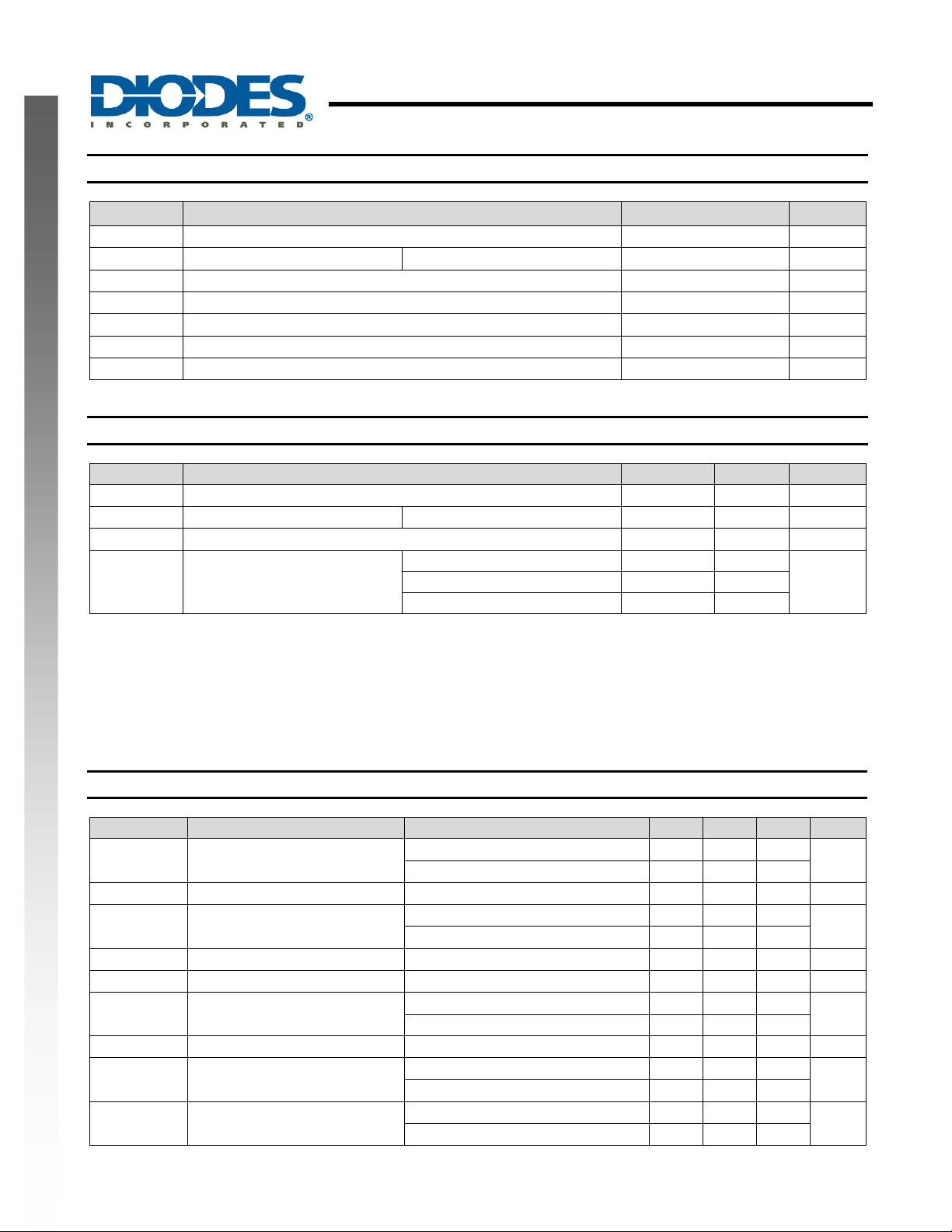
Absolute Maximum Ratings (Note 2) @ T
Symbol Parameter Rating Unit
VCC
VI
IO
θ
JA
θ
JC
TJ
T
STG
Supply voltage (Note 3) 18 V
Input voltage CONT, RESET, THRES, TRIG
Output current ±225 mA
Package thermal resistance Junction-to-Ambient
Package thermal resistance Junction-to-Case
Junction temperature 150 °C
Storage temperature -65 to 150 °C
Recommended Operating Conditions (T
Symbol Parameter Min Max Unit
VCC
VI
NEW PRODUCT
IO
TA
Notes: 2. Stresses beyond those listed under "absolute maximum ratings" may cause permanent damage to the device. These are stress ratings only.
Functional operation of the device at these or any other conditions beyond those indicated under "recommended operating conditions" is not
implied. Exposure to absolute-maximum-rated conditions for extended periods may affect device reliability.
3. All voltage values are with respect ground.
4. Maximum power dissipation is a function of T
is P
5. Maximum power dissipation is a function of T
is P
Supply voltage 4.5
Input voltage CONT, RESET, THRES, TRIG
Output current
Operating Ambient Temperature
(max), θJA, and TA. The maximum allowable power dissipation at any allowable ambient temperature
= (TJ(max) – TA)/θJA. Operating at the absolute maximum TJ of 150°C can affect reliability.
D
= (TJ(max) – TC)/θJA. Operating at the absolute maximum TJ of 150°C can affect reliability.
D
J
(max), θJC, and TA. The maximum allowable power dissipation at any allowable ambient temperature
J
Electrical Characteristics (V
= 5V to 15V, TA = 25°C unless otherwise stated)
CC
Symbol Parameter Test conditions Min Typ. Max Unit
VTH
ITH
VTR
ITR
V
RST
I
RST
I
DIS
V
DIS
V
CON
Threshold voltage level
Threshold current
(Note 6) 30 250 nA
Trigger voltage level
Trigger current TRIG at 0V 0.5 2 µA
RESET voltage level 0.3 0.7 1 V
RESET current
DISCH switch off-state current 20 100 nA
DISCH saturation voltage with
output low (Note 7)
CONT voltage (open circuit)
NE555/SA555/NA555
Document number: DS35112 Rev. 4 - 2
= 25°C unless otherwise stated
A
(Note 4) 130 °C/W
(Note 5) 15 °C/W
= 25°C)
A
NE555 0 70
SA555 -40 85
NA555 -40 105
V
= 15V
CC
V
= 5V
CC
= 15V
V
CC
V
= 5V
CC
RESET at V
CC
RESET at 0V -0.4 -1.5
= 15V, I
V
CC
VCC = 5V, I
V
= 15V
CC
V
= 5V
CC
www.diodes.com
DIS
DIS
3 of 14
= 15mA
= 4.5mA
PRECISION TIMERS
VCC
16 V
8.8 10 11.2
2.4 3.3 4.2
4.5 5 5.6
1.1 1.67 2.2
0.1 0.4
180 480
80 200
9 10 11
2.6 3.3 4
V
±200 mA
CC
February 2012
© Diodes Incorporated
V
V
°C
V
V
mA
mV
V
Page 4
NE555/SA555/NA555
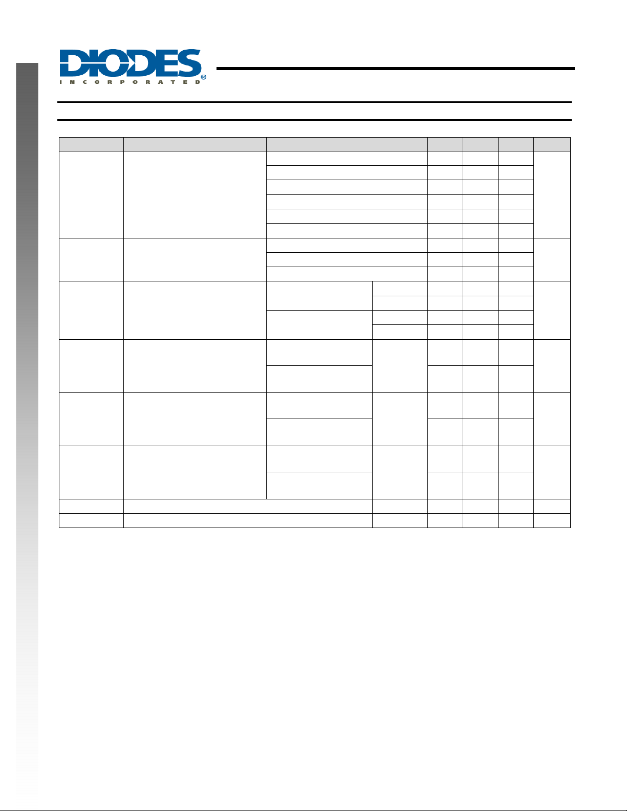
Electrical Characteristics (V
Symbol Parameter Test conditions Min Typ. Max Unit
VOL
VOH
ICC
NEW PRODUCT
TER
TTC
T
VCC
TRI
TFA
Notes: 6. This parameter influences the maximum value of the timing resistors RA and RB in the circuit of Figure 12. For example, when VCC = 5 V, the
maximum value is R = R
7. No protection against excessive pin 7 current is necessary providing package dissipation rating is not exceeded
9. Values specified are for a device in a monostable circuit similar to Figure 9, with the following component values: R
10. Values specified are for a device in an astable circuit similar to Figure 12, with the following component values: R
Low level output voltage
High level output voltage
Supply current
Initial error of timing interval
(Note 8)
Temperature coefficient of timing
interval
Supply voltage sensitivity of
timing interval
Output pulse rise time
Output pulse fall time
+ RB ≉ 3.4MΩ, and for VCC = 15 V, the maximum value is 10MΩ.
A
8. Timing interval error is defined as the difference between the measured value and the average value of a random sample from ea ch process run.
= 5V to 15V, TA = 25°C unless otherwise stated)
CC
V
= 15V, I
CC
V
= 15V, I
CC
V
= 15V, I
CC
V
= 15V, I
CC
V
= 5V, I
CC
V
= 5V, I
CC
= 15V, I
V
CC
V
= 15V, I
CC
V
= 5V, I
CC
Output low, no load
Output high, no load
Each time, monostable
(Note 9)
Each time, astable
= 10mA
OL
= 50mA
OL
= 100mA
OL
= 200mA
OL
= 5mA
OL
= 8mA
OL
= -100mA
OH
= -200mA
OH
= -100mA
OH
V
= 15V
CC
V
= 5V
CC
= 15V
V
CC
V
= 5V
CC
(Note 10)
Each time, monostable
(Note 9)
Each time, astable
T
= full
A
range
(Note 10)
Each time, monostable
(Note 9)
Each time, astable
(Note 10)
CL = 15pF
CL = 15pF
PRECISION TIMERS
0.1 0.25
0.4 0.75
2 2.5
2.5
0.1 0.35
0.15 0.4
12.75 13.3
12.5
2.75 3.3
10 15
3 6
9 13
2 5
1 3
2.25
50
150
0.1 0.5
0.3
100 300 ns
100 300 ns
= 2kΩ to 100kΩ, C = 0.1uF.
A
= 1kΩ to 100kΩ, C = 0.1uF.
A
V
V
mA
%
ppm/°C
%/V
NE555/SA555/NA555
Document number: DS35112 Rev. 4 - 2
4 of 14
www.diodes.com
February 2012
© Diodes Incorporated
Page 5
O
EVEL OUTP
O
G
E
O
OUTPU
T VOLTAG
O
OUTPU
T VOLTAG
OLTAG
ROP
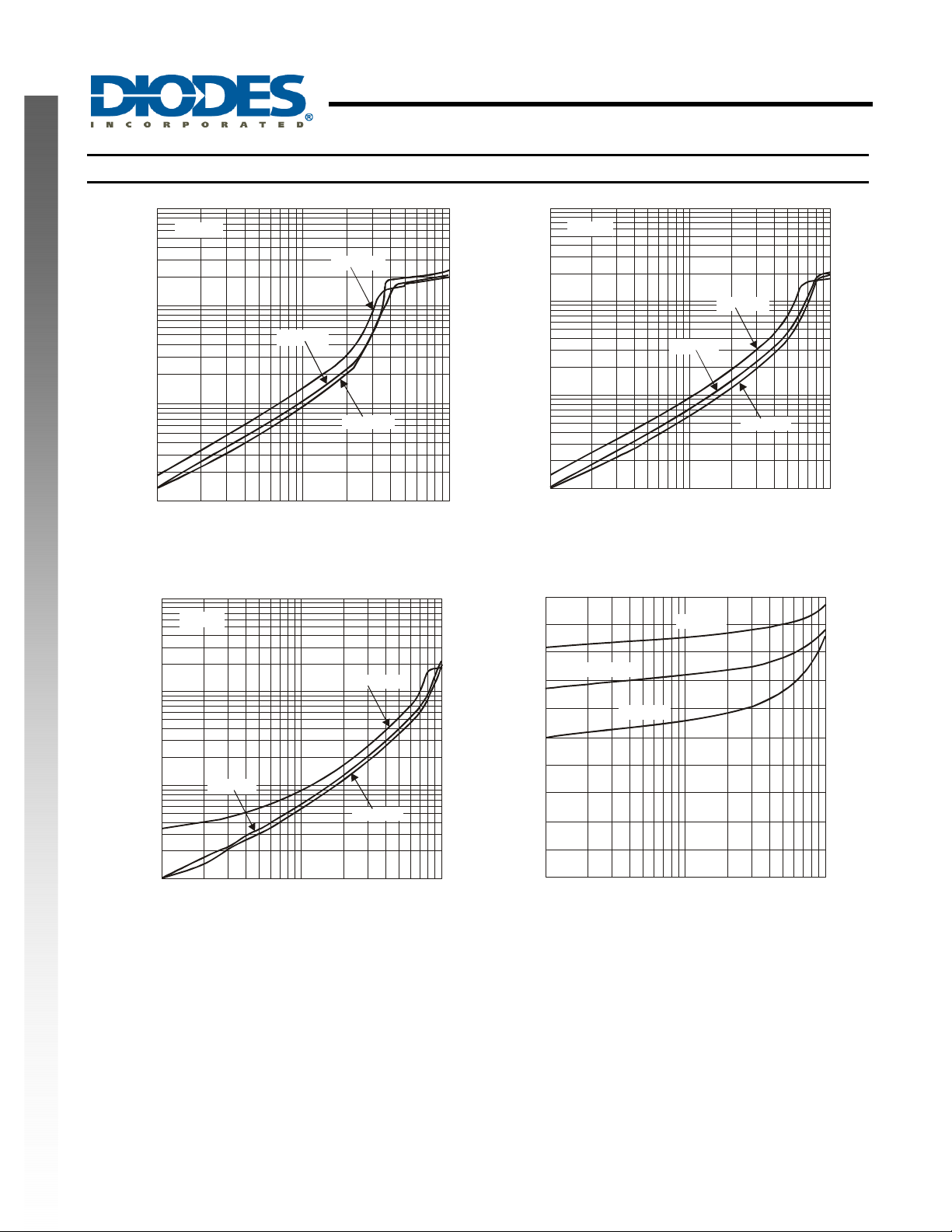
Typical Performance Characteristics
NEW PRODUCT
10
7
(V)
4
2
LTA
1
0.7
UT V
0.4
0.2
0.1
0.07
W - L
0.04
OL
0.02
V - L
0.01
12 7 701004020104
V = 5V
CC
T = 25°C
A
I - LOW LEVEL OUTPUT CURRENT (mA)
OL
Low Level Out put Voltage vs.
Low Level Output Current @ V = 5V
T = 105°C
A
T = -40°C
A
CC
NE555/SA555/NA555
PRECISION TIMERS
10
7
V = 10V
CC
4
E (V)
2
1
0.7
0.4
0.2
0.1
0.07
W - LEVEL
0.04
OL
0.02
V - L
0.01
12 7 701004020104
I - LOW LEVEL OUTPUT CURRENT (mA)
OL
Low Level Output Voltage vs.
Low Level Output Current @ V = 10V
T = 25°C
A
T = 105°C
A
T = -40°C
A
CC
10
7
4
E (V)
2
1
0.7
0.4
0.2
0.1
0.07
W - LEVEL
0.04
OL
0.02
V - L
0.01
12 7 701004020104
V = 15V
CC
T = 105°C
A
T = 25°C
A
T = -40°C
A
I - LOW LEVEL OUTPUT CURRENT (mA)
OL
Low Level Output Voltage vs.
Low Level Output Cu r r ent @ V = 15V
CC
2
1.8
1.6
(V)
1.4
1.2
E D
1
0.8
0.6
CC OH
0.4
(V - V ) V
0.2
0
12 7 701004020104
T = -40°C
A
T = 25°C
A
T = 105°C
A
V = 5V to 15V
CC
I - HIGH LEVEL OUTPUT CURRENT (mA)
OH
Drop Between Sup ply Voltage and Ou tput vs.
High Leve l Output Cur r ent
NE555/SA555/NA555
Document number: DS35112 Rev. 4 - 2
5 of 14
www.diodes.com
February 2012
© Diodes Incorporated
Page 6

P
U
U
RATIO
N R
T
U
Typical Performance Characteristics
14
Output Low, No Load
12
10
T = -40°C
A
NE555/SA555/NA555
PRECISION TIMERS
(cont.)
1000
900
800
700
NEW PRODUCT
8
6
4
CC
I - SUPPLY CURRENT (mA)
2
0
5 6 7 9 14 15131211108
1.015
1.01
1.005
1
CC
@ V = 10V
0.995
T = 105
A
T = 25
°C
A
V - SUPPLY VOLTAGE (V)
CC
Supply Cu r r ent vs. Supply Voltage
600
°C
500
400
300
200
PD
T - PROPAGATION DELAY TIME (ns)
100
1.015
E
1.01
1.005
IVE to VAL
ELA
A
@ T = 25°C
0.995
0
0 0.05 0.15 0.35 0.40.30.250.20.1
LOWEST LEVEL of TRIGGER PULSE -xV
Propagation Delay Time vs.
Lowest Volt age Level of Tr igger Pulse
1
CC
0.99
PULSE DURATION RELATIVE to VALUE
0.985
02015105
V - SUPPLY VOLTAGE (V)
CC
Normal ized Output Pulse Dur ation
(Monostable Mode) vs. Supply Voltage
LSE D
0.0985
0.99
-75 -50 0 100 125755025-25
T - FREE AIR TEMPERATURE (°C)
A
Normal ized Output Pulse Du r at io n
(Monostable Mode) vs. Free-Air Temperatu r e
NE555/SA555/NA555
Document number: DS35112 Rev. 4 - 2
6 of 14
www.diodes.com
February 2012
© Diodes Incorporated
Page 7

NE555/SA555/NA555
Typical Applications Characteristics
Monostable Operation
For monostable operation, any of the ‘555 timers can be connected as shown in Figure 1. If the output is low, application of a
negative-going pulse to the trigger (TRIG) sets the internal flip-flop and drives the output high. Capacit or C is then charged
through RA until the voltage across the capacitor reaches the thresh old voltage of the threshold (THRES) input. If TRIG has
returned to a high level, the output of the threshold comparator resets the internal flip-flop, drives the output low, and
discharges C.
NEW PRODUCT
Monostable operation is initiated when TRIG voltage falls below the trigger threshold. Once initiated, the sequenc e ends onl y
if TRIG is high for at least 10μs before the end of the timing interval. When the trigger is grounde d, the comparator storage
time can be as long as 10μs, which limits the minimum monostable pulse width to 10μs. Because of the threshold level and
saturation voltage of Q1, the output pulse duration is approximately tW = 1.1RAC. Figure 3 is a plot of the time constant for
various values of RA and C. The threshold levels and charge rates both are dir ectly proportional to the supply voltage, VCC.
The timing interval is, therefore, independent of the supply voltage, so long as the supply voltage is constant durin g the time
interval.
Applying a negative-going trigger pulse simultaneously to RESET and TRIG during the timing interval discharges C and
reinitiates the cycle, commencing on the positive edge of the reset pulse. T he output is held low as l ong as the reset pulse is
low. To prevent false triggering, when RESET is not used, it should be connected to V
Input
R
A
C
V
CC
(5V to 15V)
8
V
CC
OUT
3
4
7
6
2
5
CONT
RESET
DISCH
THRES
TRIG
GND
1
Fig 1. Monostable operation
R
L
Output
.
CC
PRECISION TIMERS
Fig. 2 Typical Monostable Waveforms
NE555/SA555/NA555
Document number: DS35112 Rev. 4 - 2
Fig. 3 Output Pulse Duration vs. Capacitance
7 of 14
www.diodes.com
February 2012
© Diodes Incorporated
Page 8

NE555/SA555/NA555
Typical Applications Characteristics (cont.)
Astable Operation
As shown in Figure 4, adding a second resistor, RB, to the circuit of Figure 1 and connecting the trigger input to the threshold
input causes the timer to self-trigger and run as a multivibrator. The capacitor C charges through R
discharges through R
This astable connection results in capacitor C charging and discharg ing between the threshold-voltag e level (≉0.67V
the trigger-voltage level (≉0.33V
and duty cycle) are independent of the supply voltage.
R
A
NEW PRODUCT
R
B
C
. Therefore, the duty cycle is controlled by the values of RA and RB.
B
). As in the monostable circuit, charge and discharge times (and, therefore, the frequency
CC
V
CC
(5V to 15V)
0.01µF
Open
(See Note A)
4
RESET
7
DISCH
6
THRES
2
TRIG
CONT
5
GND
1
V
OUT
CC
R
8
L
3
Output
PRECISION TIMERS
and RB and then
A
CC
) and
Decoupling CONT voltage to ground with a capacitor can
improve operation. This should be evaluated for individual
applications.
Fig. 4 Circuit for Astable Operation
Fig. 5 Typical Astable Waveforms
Figure 5 shows typical waveforms generated during astable operation. The output high-level duration tH and low-level
duration t
can be calculated as follows:
L
t
= 0.693(RA +RB)C
H
t
= 0.693(RB)C
L
Other useful equations are:
period = tH + tL = 0.693(RA + 2RB)C
frequency = 1.44/(R
+ 2RB)C
A
output driver duty cycle = t
/(tH + tL) = RB/(RA + 2RB)
L
output waveform duty cycle = t
/(tH + tL) = 1 – RB/(RA + 2RB)
H
low to high ratio = t
= RB/(RA + RB)
L/tH
Fig. 6 Free Running Frequency
NE555/SA555/NA555
Document number: DS35112 Rev. 4 - 2
8 of 14
www.diodes.com
February 2012
© Diodes Incorporated
Page 9

NE555/SA555/NA555
Typical Applications Characteristics (cont.)
Missing Pulse Detector
The circuit shown in Figure 7 can be used to detect a missing p ulse or abnormall y long spacing bet ween consecutive pulses
in a train of pulses. The timing interval of the monostable circuit is retriggered continuousl y by the input pulse train as long as
the pulse spacing is less than the timing interval. A longer pulse spacing, missing pulse, or terminated pulse train perm its the
timing interval to be completed, thereby generating an output pulse as shown in Figure 8.
NEW PRODUCT
PRECISION TIMERS
Fig. 7 Circuit for Missing Pulse Dectector
Frequency Divider
By adjusting the length of the timing cycle, the basic circuit of Figure 1 can be made to operate as a freq uency divider. Figur e
9 shows a divide-by-three circuit that makes use of the fact that retriggering cannot occur during the timing cycle.
Fig. 8 Timing Waveforms for Missing Pulse
Dectector
NE555/SA555/NA555
Document number: DS35112 Rev. 4 - 2
Fig. 9 Divide by Three Circuit Waveforms
9 of 14
www.diodes.com
February 2012
© Diodes Incorporated
Page 10

NE555/SA555/NA555
Typical Applications Characteristics (cont.)
Pulse Width Modulation
The operation of the timer can be modified by modulating the internal threshold and trigger volta ges, which is accomplished
by applying an external voltage (or current) to CONT. Figure 10 shows a circuit for pulse-width modulation. A cont inuous
input pulse train triggers the monostable circuit, and a control signal modulates the threshold voltage. Figure 11 shows the
resulting output pulse-width modulation. While a sine-wave modulation signal is shown, any wave shape could be used.
NEW PRODUCT
PRECISION TIMERS
Fig 10. Circuit for Pulse width modulation
Pulse Position Modulation
As shown in Figure 12, any of these timers can be used as a pulse-position modulator. This application modulates the
threshold voltage and, thereby, the time delay, of a free-runn ing oscillator. Figure 13 shows a triangular-wave modulation
signal for such a circuit; however, any wave shape could be used.
Fig 11. Pulse width modulation timing diagrams
Fig 12. Circuit for pulse position modulation
NE555/SA555/NA555
Document number: DS35112 Rev. 4 - 2
Fig 13. Pulse position modulation timing diagrams
10 of 14
www.diodes.com
February 2012
© Diodes Incorporated
Page 11

NE555/SA555/NA555
Typical Applications Characteristics (cont.)
Sequential Timer
Many applications, such as computers, require signals for initializing co nditions during start-up. Other applications, such as
test equipment, require activation of test signals in sequence. These timing circuits can be connected to provide such
sequential control. The timers can be used in various combinations of astable or monostable circuit connections, with or
without modulation, for extremely flexible waveform control. Figure 14 shows a sequencer circuit with possible applications in
many systems, and Figure 15 shows the output waveforms.
NEW PRODUCT
Fig 14. Circuit for Sequential Timer
PRECISION TIMERS
NE555/SA555/NA555
Document number: DS35112 Rev. 4 - 2
Fig 15. Sequential timer waveforms
11 of 14
www.diodes.com
February 2012
© Diodes Incorporated
Page 12

NE555/SA555/NA555
Ordering Information
XXXXX X -X
XXXXX X -X
Device
NE555S-13 0 to 70°C S SO-8 2500/Tape & Reel -13
SA555S-13 -40 to 85°C S SO-8 2500/Tape & Reel -13
NA555S-13 -40 to 105°C S SO-8 2500/Tape & Reel -13
Notes: 10. Pad layout as shown on Diodes Inc. suggested pad layout document AP02001, which can be found on our website at
http://www.diodes.com/datasheets/ap02001.pdf.
NEW PRODUCT
Operating
Temperature
Device
Device
NE555
NE555
SA555
SA555
NA555
NA555
Package
Code
Package
Package
S : SO-8
S : SO-8
Packaging
(Note 10)
Marking Information
SO-8
Packing
Packing
13 : Tape & Reel
13 : Tape & Reel
:
:
Quantity Part Number Suffix
PRECISION TIMERS
13” Tape and Reel
NE555/SA555/NA555
Document number: DS35112 Rev. 4 - 2
12 of 14
www.diodes.com
February 2012
© Diodes Incorporated
Page 13

Package Outline Dimensions (All Dimensions in mm)
SO-8
e
D
NEW PRODUCT
Suggested Pad Layout
SO-8
b
X
Y
C2
E1
E
A2
A1
Detail ‘A’
h
A3
A
L
°
45
C1
Dimensions Value (in mm)
X 0.60
Y 1.55
C1 5.4
C2 1.27
0.254
Gaug e Plane
Seating Plane
7°~9
°
Detail ‘A’
NE555/SA555/NA555
PRECISION TIMERS
Dim Min Max
SO-8
A - 1.75
A1 0.10 0.20
A2 1.30 1.50
A3 0.15 0.25
b 0.3 0.5
D 4.85 4.95
E 5.90 6.10
E1 3.85 3.95
e 1.27 Typ
h - 0.35
L 0.62 0.82
0° 8°
θ
All Dimensions in mm
NE555/SA555/NA555
Document number: DS35112 Rev. 4 - 2
13 of 14
www.diodes.com
February 2012
© Diodes Incorporated
Page 14

NE555/SA555/NA555
PRECISION TIMERS
NEW PRODUCT
IMPORTANT NOTICE
DIODES INCORPORATED MAKES NO WARRANTY OF ANY KIND, EXPRESS OR IMPLIED, WITH REGARDS TO THIS
DOCUMENT, INCLUDING, BUT NOT LIMITED TO, THE IMPLIED WARRANTIES OF MERCHANTABILITY AND FITNESS FOR A
PARTICULAR PURPOSE (AND THEIR EQUIVALENTS UNDER THE LAWS OF ANY JURISDICTION).
Diodes Incorporated and its subsidiaries reserve the right to make modifications, enhancements, improvements, corrections or other
changes without further notice to this document and any product described herein. Diodes Incorporated does not assume any liability
arising out of the application or use of this document or any product described herein; neither does Diodes Incorporated convey any
license under its patent or trademark rights, nor the rights of others. Any Customer or user of this document or products described
herein in such applications shall assume all risks of such use and will agree to hold Diodes Incorporated and all the companies
whose products are represented on Diodes Incorporated website, harmless against all damages.
Diodes Incorporated does not warrant or accept any liability whatsoever in respect of any products purchased through unauthorized
sales channel.
Should Customers purchase or use Diodes Incorporated products for any unintended or unauthorized application, Customers shall
indemnify and hold Diodes Incorporated and its representatives harmless against all claims, damages, expenses, and attorney fees
arising out of, directly or indirectly, any claim of personal injury or death associated with such unintended or unauthorized application.
Products described herein may be covered by one or more United States, international or foreign patents pending. Product names
and markings noted herein may also be covered by one or more United States, international or foreign trademarks.
LIFE SUPPORT
Diodes Incorporated products are specifically not authorized for use as critical components in life support devices or systems without
the express written approval of the Chief Executive Officer of Diodes Incorporated. As used herein:
A. Life support devices or systems are devices or systems which:
1. are intended to implant into the body, or
2. support or sustain life and whose failure to perform when properly used in accordance with instructions for use provided
in the labeling can be reasonably expected to result in significant injury to the user.
B. A crit ical component is any component in a life support device or system whose failure to perform can be reasonably expected
to cause the failure of the life support device or to affect its safety or effectiveness.
Customers represent that they have all necessary expertise in the safety and regulatory ramifications of their life support devices or
systems, and acknowledge and agree that they are solely responsible for all legal, regulatory and safety-related requirements
concerning their products and any use of Diodes Incorporated products in such safety-critical, life support devices or systems,
notwithstanding any devices- or systems-related information or support that may be provided by Diodes Incorporated. Further,
Customers must fully indemnify Diodes Incorporated and its representatives against any damages arising out of the use of Diodes
Incorporated products in such safety-critical, life support devices or systems.
Copyright © 2012, Diodes Incorporated
www.diodes.com
NE555/SA555/NA555
Document number: DS35112 Rev. 4 - 2
14 of 14
www.diodes.com
February 2012
© Diodes Incorporated
 Loading...