

Page 1
A
A
Features
Dual TVS in Common Cathode Configuration for ESD Protection
40 Watt Peak Power Dissipation @1.0ms (Unidirectional)
225mW Power Dissipation
Ideally Suited for Automated Insertion
Low Leakage
Totally Lead-Free & Fully RoHS Compliant (Notes 1 & 2)
Halogen and Antimony Free. “Green” Device (Note 3 & 4)
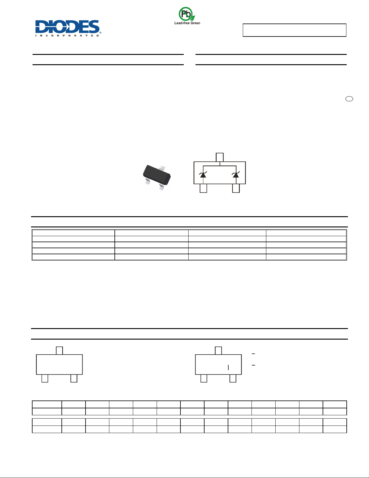
SOT23
Top View
MMBZ15VDL, MMBZ27VCL
40W PEAK POWER DUAL SURFACE MOUNT TVS
Mechanical Data
Case: SOT23
Case Material: Molded Plastic. UL Flammability Rating
Classification 94V-0
Moisture Sensitivity: Level 1 per J-STD-020
Terminals: Solderable per MIL-STD-202, Method 208 Lead Free
Plating (Matte Tin Finish annealed over Alloy 42 leadframe).
Polarity: See Diagram
Weight: 0.008 grams (approximate)
Device Schematic
e3
Ordering Information (Note 5 & 6)
Part Number Compliance Case Packaging
MMBZ15VDL-7-F Standard SOT23 3000/Tape & Reel
MMBZ27VCL-7-F Standard SOT23 3000/Tape & Reel
MMBZ15VDLQ-7-F Automotive SOT23 3000/Tape & Reel
MMBZ27VCLQ-7-F Automotive SOT23 3000/Tape & Reel
Notes: 1. No purposely added lead. Fully EU Directive 2002/95/EC (RoHS) & 2011/65/EU (RoHS 2) compliant.
2. See http://www.diodes.com/quality/lead_free.html for more information about Diodes Incorporated’s definitions of Halogen- and Antimony-free, "Green"
and Lead-free.
3. Halogen- and Antimony-free "Green” products are defined as those which contain <900ppm bromine, <900ppm chlorine (<1500ppm total Br + Cl) and
<1000ppm antimony compounds.
Code V9 are built with Non-Green Molding Compound and may contain Halogens or Sb
the same, except where specified.
4. Product manufactured with Date Code V9 (week 33, 2008) and newer are built with Green Molding Compound. Product manufactured prior to Date
5. Automotive products are AEC-Q101 qualified and are PPAP capable. Automotive, AEC-Q101 and standard products are electrically and thermally
6. For packaging details, go to our website at http://www.diodes.com/products/packages.html.
Fire Retardants.
2O3
Marking Information
Kxx
Date Code Key
Year 2006 2007 2008 2009 2010 2011 2012 2013 2014 2015 2016 2017
Code T U V W X Y Z A B C D E
Month Jan Feb Mar Apr May Jun Jul Aug Sep Oct Nov Dec
Code 1 2 3 4 5 6 7 8 9 O N D
xx = Product Type Marking Code
YM = Date Code Marking for Shanghai
YM
ssembly / Test site
Y = Year (ex: A = 2013)
M = Month (ex: 9 = September)
Kxx
xx = Product Type Marking Code
= Date Code Marking for Chengdu
YM
ssembly / Test site
= Year (ex: A = 2013)
Y
YM
M = Month (ex: 9 = September)
MMBZ15VDL, MMBZ27VCL
Document number: DS30352 Rev. 15 - 2
1 of 5
www.diodes.com
October 2013
© Diodes Incorporated
Page 2
P
P
U
R
T
N
G
N
O
MMBZ15VDL, MMBZ27VCL
Maximum Ratings (@T
= +25°C, unless otherwise specified.)
A
Characteristic Symbol Value Unit
Peak Power Dissipation (Note 7)
P
PK
40 W
Thermal Characteristics
Characteristic Symbol Value Unit
Power Dissipation (Note 8)
Thermal Resistance, Junction to Ambient Air (Note 8)
Operating and Storage Temperature Range
P
D
R
JA
T
, T
J
STG
Electrical Characteristics (@T
= +25°C, unless otherwise specified.)
A
VF = 0.9V max @ IF = 10mA
Breakdown Voltage
VBR (Note 9) (V) @ IT V
Type
Number
Marking
Code
Max
Reverse
Leakage I
@ V
RWM
R
V
RWM
(Note 9)
Volts nA Min Nom Max mA V A TC (%/°C)
MMBZ15VDL KVJ 12.8 100 14.3 15 15.8 1.0 21.2 1.9 +0.080
VF = 1.1V max @ IF = 200mA
Type
Number
Marking
Code
V
RWM
Max
Reverse
Leakage I
@ V
RWM
R
(Note 9)
Volts nA Min Nom Max mA V A TC (%/°C)
MMBZ27VCL KVP 22 50 25.65 27 28.35 1.0 38 1.0 +0.090
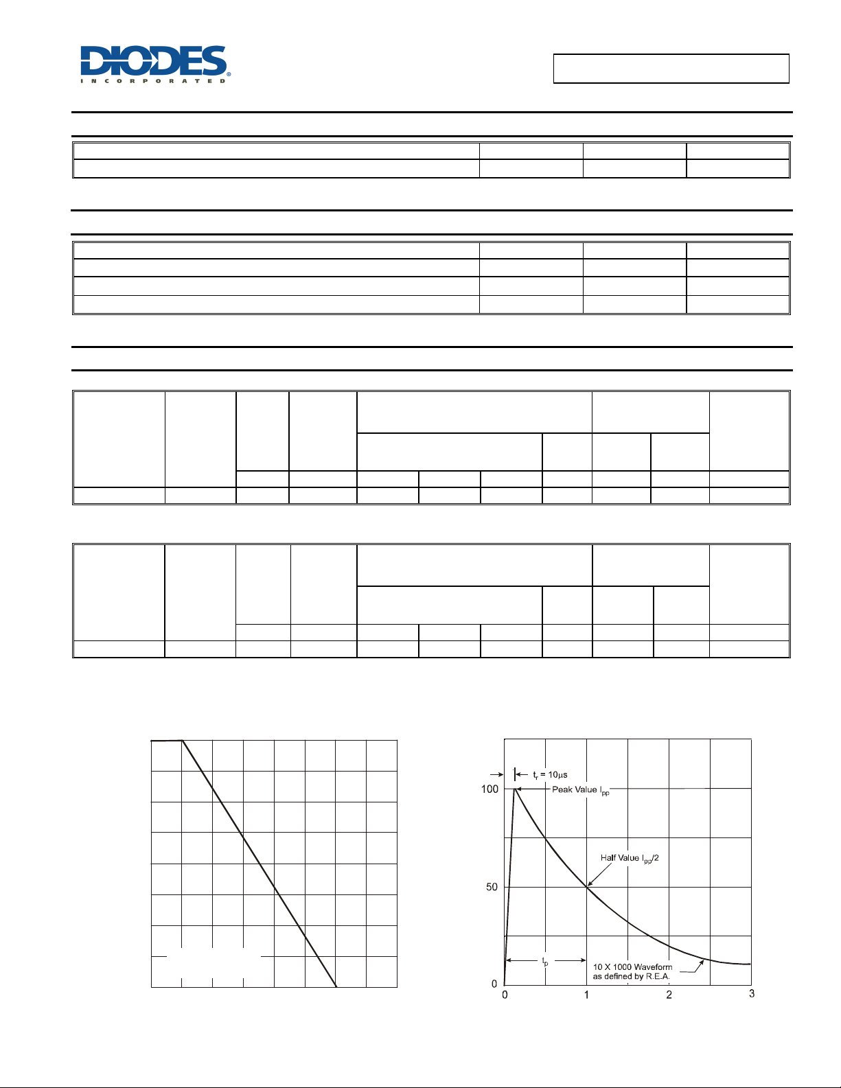
Notes: 7. Non-repetitive current pulse per Figure 2 and derate above TA = +25°C per Figure 1.
8. Device mounted on FR-5 PCB 1.0 x 0.75 x 0.062 inch pad layout as shown on Diodes Inc. suggested pad layout AP02001, which can be found on our
website at http://www.diodes.com. 200mW per element must not be exceeded.
9. Short duration pulse test used to minimize self-heating effect.
100
Breakdown Voltage
VBR (Note 9) (V) @ IT V
225 mW
556 °C/W
-65 to +150 °C
Max. Clamping
Voltage V
C @ IPP
(Note 7)
I
C
PP
Typical
Temperature
Coefficient
Max. Clamping
Voltage V
C @ IPP
(Note 7)
I
C
PP
Typical
Temperature
Coefficient
F
%
75
I
I
A
50
LSE DE
25
PEAK POWER OR CURRENT
EAK
10 X 1000 Waveform
as defined by REA
PP pp
I , PEAK PULSE CURRENT (%I )
0
0 25 50 75 100 125 150 175 200
T , AMBIENT TEMPERATURE ( C)
A
°
Figure 1 Pulse Derating Curve
MMBZ15VDL, MMBZ27VCL
Document number: DS30352 Rev. 15 - 2
2 of 5
www.diodes.com
t, TIME (ms)
Figure 2 Pulse Waveform
October 2013
© Diodes Incorporated
Page 3

P, P
OWER
PATIO
R
O
O
TAG
GE CUR
RENT
MMBZ15VDL, MMBZ27VCL
300
Note 8
250
30
29
E (V)
N (mW)
200
150
DISSI
100
D
FR-5 Board
50
0
025
T , AMBIENT TEMPERATURE
A
75 100 125 150
50
Figure 3 Steady State Power Derating Curve
175
L
WN V
EAKD
BR
V, B
28
27
26
25
-55
-15
T , AMBIENT TEMPERATURE (°C)
A
25
Figure 4 Typical Breakdown Voltage vs.
65
105 145
Temperature (MMBZ27VCL)
100
100
T = 25°C
J
(nA)
I , LEAKA
R
100
0.1
10
10
Unidirectional
1
-55
-15
T , AMBIENT TEMPERATURE (°C)
A
25 65 105
Figure 5 Typical Leakage Current vs.
Temperature (MMBZ27VCL)
Bidirectional
Unidirectional
T = 25CJ°
Non repetitive
pulse waveform
(Rectangular)
145
Bidirectional
10
Unidirectional
Non repetitive
pulse waveform
(Rectangular)
1.0
pk
P , PEAK PULSE POWER (W)
0.1
0.1 1.0
10 100
1,000 10,000
PULSE WIDTH (ms)
Figure 6 Pulse Rating Curve, P (W) vs. Pulse Width (ms)
Power is defined as P = V x I
pk
pk C pp
1.0
pk (NOM)
P , PEAK PULSE POWER (W)
0.1
0.1 1.0
10 100
1,000 10,000
PULSE WIDTH (ms)
Figure 7 Pulse Rating Curve, P (W) vs. Pulse Width (ms)
Power is defined as P = V x I
where V is the nominal breakdown voltage
BR(NOM)
MMBZ15VDL, MMBZ27VCL
Document number: DS30352 Rev. 15 - 2
pk (NOM)
pk(NOM) BR(NOM) pp
3 of 5
www.diodes.com
October 2013
© Diodes Incorporated
Page 4

Package Outline Dimensions
Please see AP02002 at http://www.diodes.com/datasheets/ap02002.pdf for the latest version.
K
J
A
Dim Min Max Typ
A 0.37 0.51 0.40
B 1.20 1.40 1.30
C
B
C 2.30 2.50 2.40
D 0.89 1.03 0.915
F 0.45 0.60 0.535
G 1.78 2.05 1.83
H
H 2.80 3.00 2.90
J 0.013 0.10 0.05
K1
F
D
G
L
M
K 0.903 1.10 1.00
K1 - - 0.400
L 0.45 0.61 0.55
M 0.085 0.18 0.11
Suggested Pad Layout
Please see AP02001 at http://www.diodes.com/datasheets/ap02001.pdf for the latest version.
Y
Dimensions Value (in mm)
Z 2.9
Z
C
X 0.8
Y 0.9
C 2.0
E 1.35
X
E
MMBZ15VDL, MMBZ27VCL
SOT23
0° 8° -
All Dimensions in mm
MMBZ15VDL, MMBZ27VCL
Document number: DS30352 Rev. 15 - 2
4 of 5
www.diodes.com
October 2013
© Diodes Incorporated
Page 5

IMPORTANT NOTICE
DIODES INCORPORATED MAKES NO WARRANTY OF ANY KIND, EXPRESS OR IMPLIED, WITH REGARDS TO THIS DOCUMENT,
INCLUDING, BUT NOT LIMITED TO, THE IMPLIED WARRANTIES OF MERCHANTABILITY AND FITNESS FOR A PARTICULAR PURPOSE
(AND THEIR EQUIVALENTS UNDER THE LAWS OF ANY JURISDICTION).
Diodes Incorporated and its subsidiaries reserve the right to make modifications, enhancements, improvements, corrections or other changes
without further notice to this document and any product described herein. Diodes Incorporated does not assume any liability arising out of the
application or use of this document or any product described herein; neither does Diodes Incorporated convey any license under its patent or
trademark rights, nor the rights of others. Any Customer or user of this document or products described herein in such applications shall assume
all risks of such use and will agree to hold Diodes Incorporated and all the companies whose products are represented on Diodes Incorporated
website, harmless against all damages.
Diodes Incorporated does not warrant or accept any liability whatsoever in respect of any products purchased through unauthorized sales channel.
Should Customers purchase or use Diodes Incorporated products for any unintended or unauthorized application, Customers shall indemnify and
hold Diodes Incorporated and its representatives harmless against all claims, damages, expenses, and attorney fees arising out of, directly or
indirectly, any claim of personal injury or death associated with such unintended or unauthorized application.
Products described herein may be covered by one or more United States, international or foreign patents pending. Product names and markings
noted herein may also be covered by one or more United States, international or foreign trademarks.
This document is written in English but may be translated into multiple languages for reference. Only the English version of this document is the
final and determinative format released by Diodes Incorporated.
LIFE SUPPORT
Diodes Incorporated products are specifically not authorized for use as critical components in life support devices or systems without the express
written approval of the Chief Executive Officer of Diodes Incorporated. As used herein:
A. Life support devices or systems are devices or systems which:
1. are intended to implant into the body, or
2. support or sustain life and whose failure to perform when properly used in accordance with instructions for use provided in the
labeling can be reasonably expected to result in significant injury to the user.
B. A critical component is any component in a life support device or system whose failure to perform can be reasonably expected to cause the
failure of the life support device or to affect its safety or effectiveness.
Customers represent that they have all necessary expertise in the safety and regulatory ramifications of their life support devices or systems, and
acknowledge and agree that they are solely responsible for all legal, regulatory and safety-related requirements concerning their products and any
use of Diodes Incorporated products in such safety-critical, life support devices or systems, notwithstanding any devices- or systems-related
information or support that may be provided by Diodes Incorporated. Further, Customers must fully indemnify Diodes Incorporated and its
representatives against any damages arising out of the use of Diodes Incorporated products in such safety-critical, life support devices or systems.
Copyright © 2013, Diodes Incorporated
www.diodes.com
MMBZ15VDL, MMBZ27VCL
MMBZ15VDL, MMBZ27VCL
Document number: DS30352 Rev. 15 - 2
5 of 5
www.diodes.com
October 2013
© Diodes Incorporated
 Loading...