DIODES MMBTA28 Datasheet

Features
TCUDORPWEN
· Epitaxial Planar Die Construction
· Ideal for Medium Power Amplification and
Switching
· High Current Gain
Mechanical Data
· Case: SOT-23, Molded Plastic
· Case Material - UL Flammability Rating
Classification 94V-0
· Moisture sensitivity: Level 1 per J-STD-020A
· Terminals: Solderable per MIL-STD-202,
Method 208
· Terminal Connections: See Diagram
· Marking (See Page 2): K6R
· Weight: 0.008 grams (approx.)
· Ordering & Date Code Information: See Page 2
MMBTA28
NPN SURFACE MOUNT DARLINGTON TRANSISTOR
SOT-23
E
B
B
C
TOP VIEW
G
H
C
A
B
C
E
D
K
J
D
E
L
M
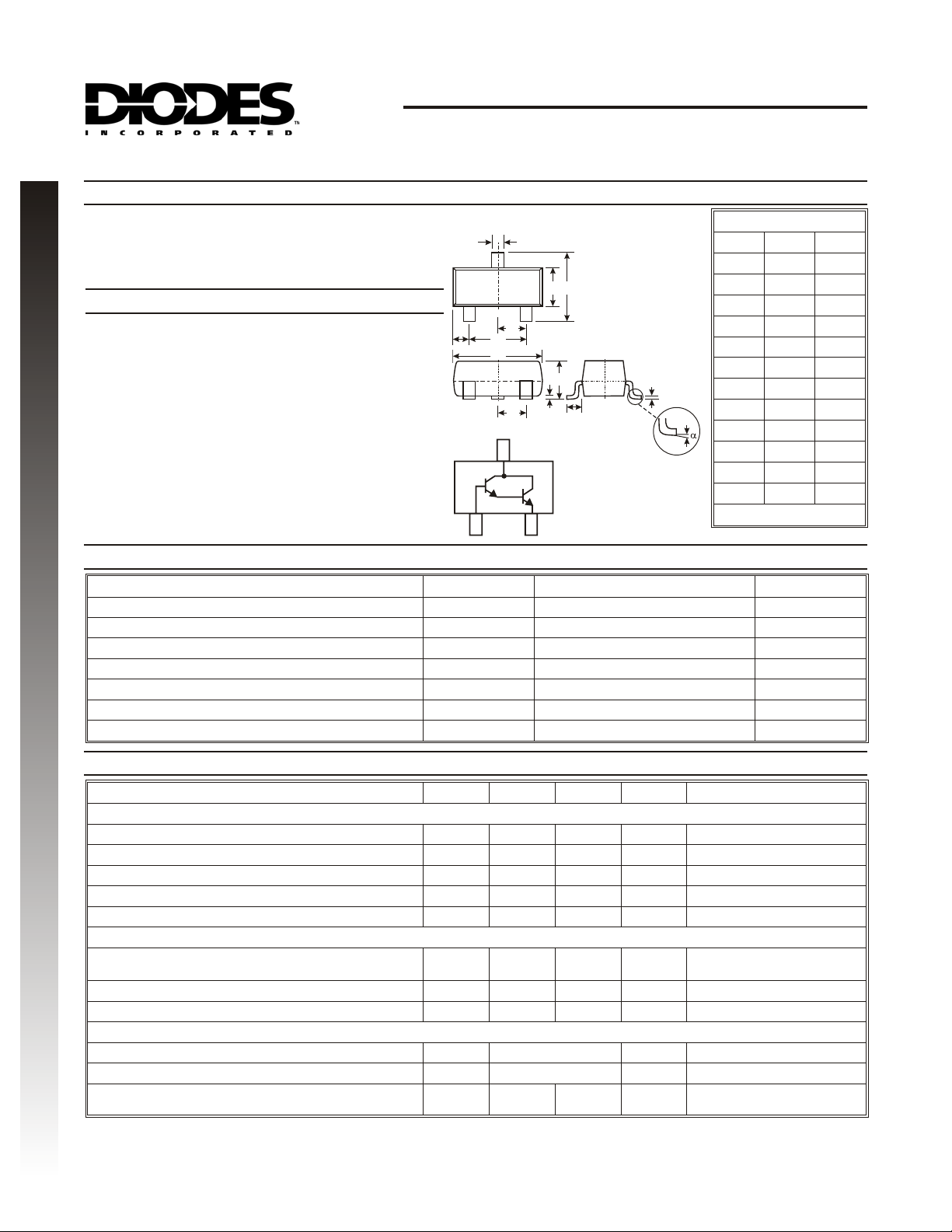
Dim Min Max
A
0.37 0.51
B
1.20 1.40
C
2.30 2.50
D
0.89 1.03
E
0.45 0.60
G
1.78 2.05
H
2.80 3.00
J
0.013 0.10
K
0.903 1.10
L
0.45 0.61
M
0.085 0.180
a
0° 8°
All Dimensions in mm
Maximum Ratings
@ TA= 25°C unless otherwise specified
Characteristic Symbol MMBTA28 Unit
Collector-Base Voltage
Collector-Emitter Voltage
Emitter-Base Voltage
Collector Current - Continuous
Power Dissipation
Thermal Resistance, Junction to Ambient
Operating and Storage and Temperature Range
Electrical Characteristics
@ TA = 25°C unless otherwise specified
Characteristic Symbol Min Max Unit Test Condition
OFF CHARACTERISTICS (Note 2)
Collector-Base Breakdown Voltage
Emitter-Base Breakdown Voltage
Collector-Emitter Breakdown Voltage
Collector Cutoff Current
Emitter Cutoff Current
ON CHARACTERISTICS (Note 2)
DC Current Gain
Collector-Emitter Saturation Voltage
Base- Emitter Saturation Voltage
SMALL SIGNAL CHARACTERISTICS
Output Capacitance
Input Capacitance
Current Gain-Bandwidth Product
V
(BR)CBO
V
(BR)EBO
V
(BR)CEO
I
CBO
I
EBO
h
V
CE(SAT)
V
BE(SAT)
C
C
Tj,T
FE
obo
ibo
f
T
V
CBO
V
CEO
V
EBO
I
C
P
d
R
qJA
STG
80 ¾ V
12 ¾ V
80 ¾ V
¾ 100 nA
¾ 100 nA
10,000
10,000
¾¾
¾ 1.5 V
¾ 2.0 V
8.0 Typical pF
15 Typical pF
125 ¾ MHz
80 V
80 V
12 V
500 mA
300
mW
417 °C/W
-55 to +150 °C
I
= 100mAIE = 0
C
= 100mAIC = 0
I
E
= 100mAIB = 0
I
C
VCB = 60V, IE= 0
VEB= 10V, IC = 0
I
= 10mA, VCE= 5.0V
C
IC = 100mA, VCE = 5.0V
IC = 100mA, IB = 100mA
IC = 100mA, VCE = 5.0V
VCB = 10V, f = 1.0MHz, IE = 0
VEB = 0.5V, f = 1.0MHz, IC = 0
= 5.0V, IC = 10mA,
V
CE
f = 100MHz
Notes: 1. Device mounted on FR-4 PCB, 1.6x1.6x0.06 nch pad layout as shown on Diodes Inc. suggested pad layout
document AP02001 which can be found on our website at http://www.diodes.com/datasheets/ap02001.pdf.
2. Short duration test pulse used to minimize self-heating effect.
DS30367 Rev. 2 - 2 1 of 3 MMBTA28
www.diodes.com

Ordering Information
p
1.1
(Note 3)
TCUDORPWEN
Device
MMBTA28-7
Packaging Shipping
SOT-23 3000/Tape & Reel
Notes: 3. For Packaging Details, go to our website at http://www.diodes.com/datasheets/ap02007.pdf.
Marking Information
K6R = Product Type Marking Code
YM = Date Code Marking
Y = Year ex: N = 2002
M = Month ex: 9 = September
2005 2006 2007 2008 2009
STUVW
Date Code Key
Month Jan Feb March Apr May Jun Jul
Code
K6R
YM
Year 2002 2003 2004
Code
NPR
1234567
Aug Sep Oct Nov Dec
89 OND
D
P , POWER DISSIPATION (mW)
350
300
250
200
150
100
50
I
1.0
C
I
B
= 1000
T = -50°C
A
0.9
0.8
T = 25°C
0.7
0.6
0.5
A
T = 150°C
A
0.4
0.3
VOLTAGE (V)
0.2
0.1
CE(SAT)
V , COLLECTOR-EMITTER SATURATION
0
0
25 50
T , AMBIENT TEMPERATURE (°C)
A
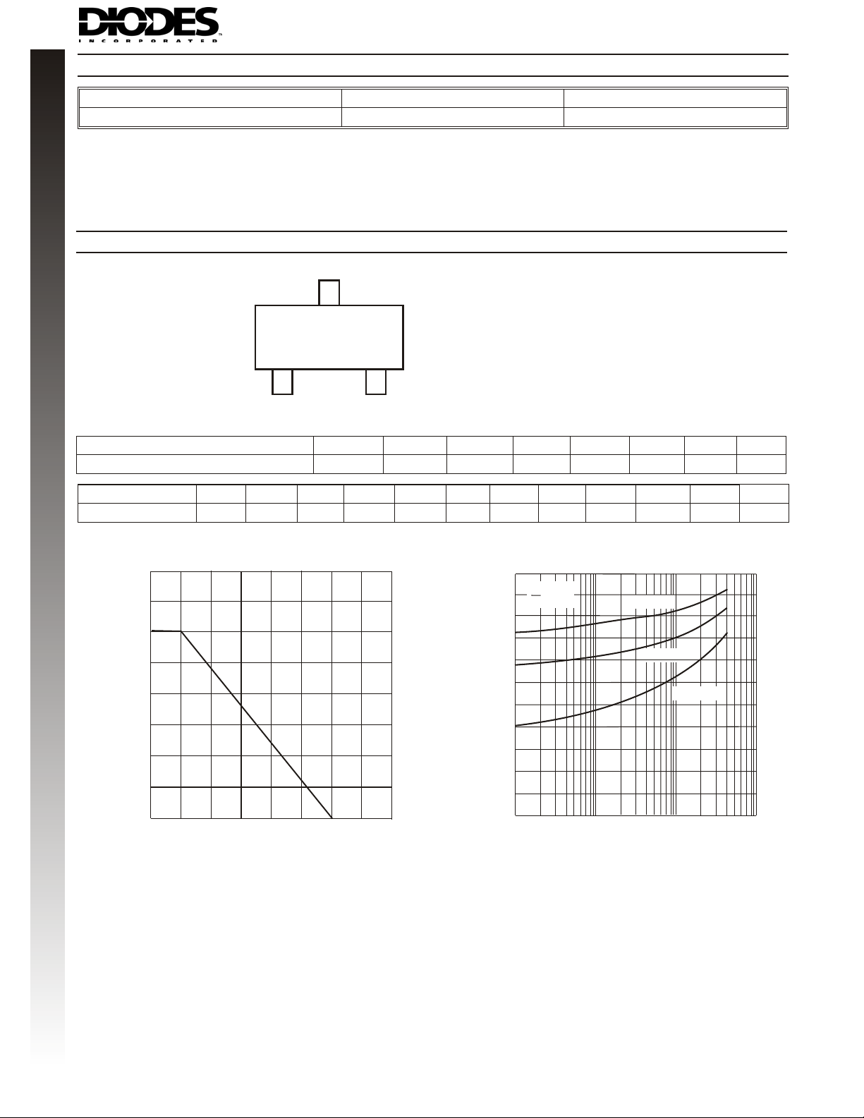
Fig. 1, Max Power Dissipation vs
100 125
75
Ambient Tem
150
erature
175
200
0
1
10
I , COLLECTOR CURRENT (mA)
C
100 1000
Fig. 2 Typical Collector-Emitter Saturation Voltage
vs. Collector Current
DS30367 Rev. 2 - 2 2 of 3 MMBTA28
www.diodes.com
 Loading...