Diodes MMBT4403 User Manual

40V PNP SURFACE MOUNT SMALL SIGNAL TRANSISTOR IN SOT23
Features
• Epitaxial Planar Die Construction
• Complementary NPN Type Available (MMBT4401)
• Ideal for Medium Power Amplification and Switching
• Totally Lead-Free & Fully RoHS compliant (Notes 1 & 2)
• Halogen and Antimony Free. “Green” Device (Note 3)
• Qualified to AEC-Q101 Standards for High Reliability
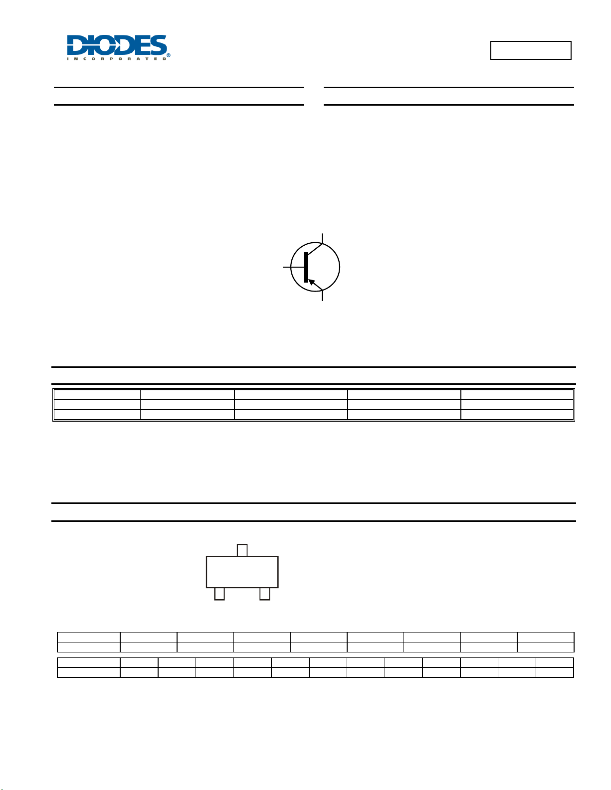
SOT23
Top View
B
Device Symbol
Mechanical Data
• Case: SOT23
• UL Flammability Rating 94V-0
• Case material: molded Plastic “Green” Compound
• Moisture Sensitivity: Level 1 per J-STD-020
• Terminals: Matte Tin Finish
• Weight: 0.008 grams (Approximate)
C
E
Top View
Pin-Out
MMBT4403
Ordering Information (Note 4)
Product Marking Reel size (inches) Tape width (mm) Quantity per reel
MMBT4403-7-F K2T 7 8 3,000
MMBT4403-13-F K2T 13 8 10,000
Notes: 1. No purposely added lead. Fully EU Directive 2002/95/EC (RoHS) & 2011/65/EU (RoHS 2) compliant.
3. Halogen and Antimony free "Green” products are defined as those which contain <900ppm bromine, <900ppm chlorine (<1500ppm total Br + Cl) and
4. For packaging details, go to our website at http://www.diodes.com
2. See http://www.diodes.com for more information about Diodes Incorporated’s definitions of Halogen and Antimony free,"Green" and Lead-Free.
<1000ppm antimony compounds.
Marking Information
Date Code Key
Year 2010 2011 2012 2013 2014 2015 2016 2017
Code X Y Z A B C D E
Month Jan Feb Mar Apr May Jun Jul Aug Sep Oct Nov Dec
Code 1 2 3 4 5 6 7 8 9 O N D
K2T
YM
MMBT4403
Document Number: DS30058 Rev. 11 - 2
K2T = Product Type Marking Code
YM = Date Code Marking
Y = Year (ex: Y = 2011)
M = Month (ex: 9 = September)
1 of 6
www.diodes.com
March 2012
© Diodes Incorporated

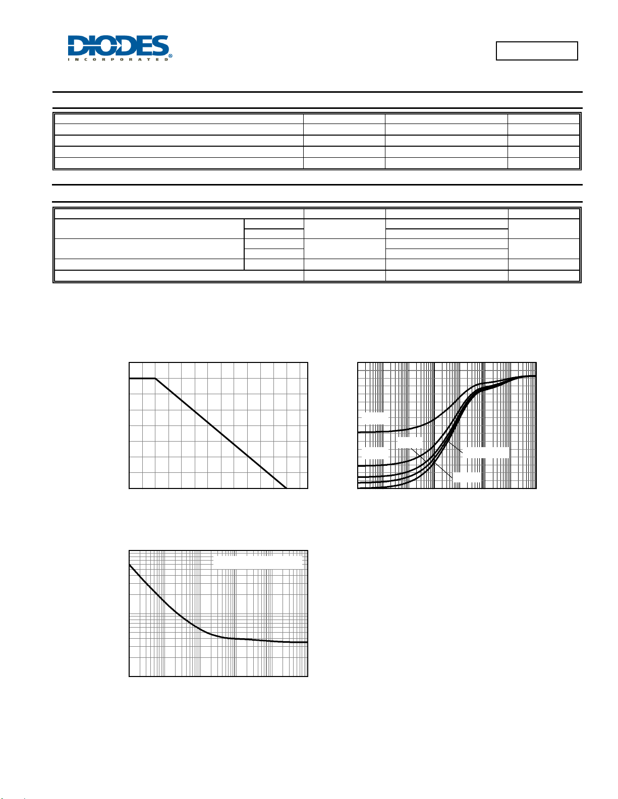
Maximum Ratings (@T
Characteristic Symbol Value Unit
Collector-Base Voltage
Collector-Emitter Voltage
Emitter-Base Voltage
Collector Current - Continuous (Note 7)
Thermal Characteristics (@T
Collector Power Dissipation
Thermal Resistance, Junction to Ambient
Thermal Resistance, Junction to Leads (Note 7)
Operating and Storage Temperature Range
Notes: 5. For the device mounted on minimum recommended pad layout FR4 PCB with high coverage of single sided 1oz copper, in still air conditions.
6. For the device mounted on 15mm x 15mm x 1.6mm FR4 PCB with high coverage of single sided 1oz copper, in still air conditions.
7. Thermal resistance from junction to solder-point (at the end of the collector lead).
= +25°C, unless otherwise specified.)
A
V
CBO
V
CEO
V
EBO
I
C
= +25°C, unless otherwise specified.)
A
Characteristic Symbol Value Unit
(Note 5)
(Note 6) 350
(Note 5)
(Note 6) 357
R
R
T
J,TSTG
P
θJA
θJL
D
-40 V
-40 V
-6.0 V
-600 mA
310
403
350
-55 to +150
MMBT4403
mW
°C/W
°C/W
°C
0.4
0.3
0.2
0.1
0.0
0 255075100125150
Max Pow e r Dissipat ion (W)
Temperature (°C)
Derating Curve
10
Single Pulse. T
1
amb
=25°C
400
350
300
250
D=0.5
200
150
D=0.2
100
50
0
100µ 1m 10m 100m 1 10 100 1k
Therma l R esistance (°C/W)
D=0.1
Single Pulse
D=0.05
Puls e Width (s)
Transient Thermal Impedance
0.1
10m 100m 1 10 100 1k
Max Power Dissipat i on (W)
Puls e Width (s)
Pulse Power Dissipation
MMBT4403
Document Number: DS30058 Rev. 11 - 2
2 of 6
www.diodes.com
March 2012
© Diodes Incorporated
 Loading...