

Page 1
Please click here to visit our online spice models database.
Features
• Low Forward Voltage Drop
• Fast Switching
• Very High Density (Five Diode Elements in a Sub-Miniature
Package)
• Lead Free/RoHS Compliant (Note 1)
• "Green" Device (Note 2)
• Qualified to AEC-Q101 Standards for High Reliability
NEW PRODUCT
Maximum Ratings @T
= 25°C unless otherwise specified
A
Characteristic Symbol Value Unit
Non-Repetitive Peak Reverse Voltage
Peak Repetitive Reverse Voltage
Working Peak Reverse Voltage
DC Blocking Voltage
RMS Reverse Voltage
Forward Continuous Current
Average Rectified Output Current
Non-Repetitive Peak Forward Surge Current @ t = 1.0μs
@ t = 1.0s
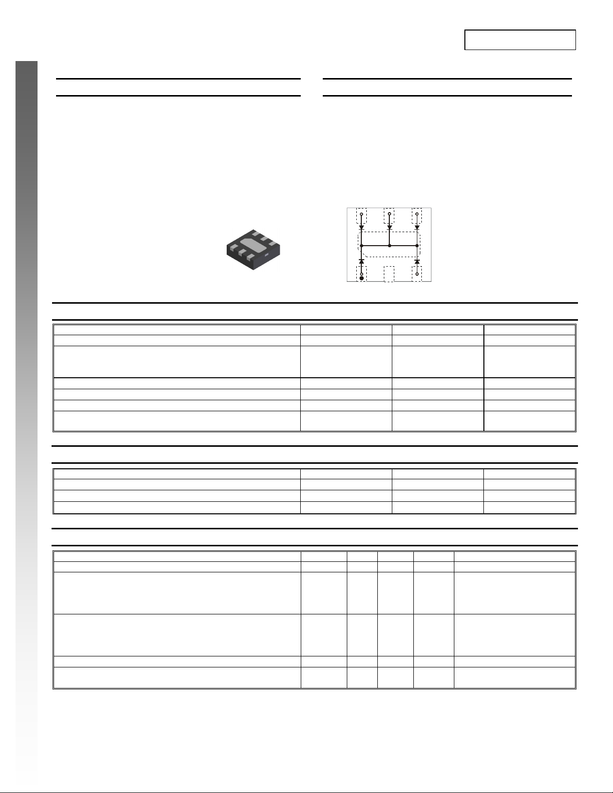
BOTTOM VIEW
MMBD4148PLM
FIVE ELEMENT COMMON CATHODE SWITCHING DIODE ARRAY
Mechanical Data
• Case: DFN1616-6
• Case Material: Molded Plastic, “Green” Molding Compound.
UL Flammability Classification Rating 94V-0
• Moisture Sensitivity: Level 1 per J-STD-020D
• Terminals: Solderable per MIL-STD-202, Method 208
• Lead Free Plating (NiPdAu Finish over Copper leadframe).
• Polarity: Pin 1 Dot and Center Pad notch, See diagram
• Marking Information: See Page 2
• Ordering Information: See Page 2
• Weight: 0.004 grams (approximate)
DFN1616-6
N/A
TOP VIEW
Internal Schematic
V
V
V
V
R(RMS)
I
RM
RRM
RWM
V
R
I
FM
I
O
FSM
100 V
75 V
53 V
300 mA
200 mA
2.0
1.0
A
Thermal Characteristics
Characteristic Symbol Value Unit
Power Dissipation (Note 3)
Thermal Resistance Junction to Ambient Air (Note 3)
Operating and Storage Temperature Range
Electrical Characteristics @T
Characteristic Symbol Min Max Unit Test Condition
Reverse Breakdown Voltage (Note 4)
Forward Voltage
Leakage Current (Note 4)
Total Capacitance
Reverse Recovery Time
Notes: 1. No Purposefully added Lead.
2. Diodes Inc.'s "Green" policy can be found on our website at http://www.diodes.com/products/lead_free/index.php.
Only one switching diode powered on.
MMBD4148PLM
Document number: DS31437 Rev. 6 - 2
3. Part mounted on FR-4 PC board with recommended pad layout, which can be found on our website at http://www.diodes.com/datasheets/ap02001.pdf.
4. Short duration pulse test used to minimize self-heating effect.
= 25°C unless otherwise specified
A
P
D
R
θ
, T
T
J
V
(BR)R
V
F
I
R
C
⎯
T
t
⎯
rr
1 of 3
www.diodes.com
JA
STG
75
⎯
0.715
0.855
⎯
1.0
1.25
1.0
⎯
50
30
25
2.0 pF
4.0 ns
500 mW
256
-65 to +150
V
V
μA
μA
μA
nA
IR = 100μA
I
= 1.0mA
F
= 10mA
I
F
I
= 50mA
F
= 150mA
I
F
V
= 75V
R
= 75V, TJ = 150°C
V
R
V
= 25V, TJ = 150°C
R
= 20V
V
R
°C/W
°C
VR = 0, f = 1.0MHz
= IR = 10mA,
I
F
= 0.1 x IR, RL = 100Ω
I
rr
September 2008
© Diodes Incorporated
Page 2
P, P
OWER
P
T
O
TANT
O
U
O
RWAR
C
URRENT
TANT
O
US R
R
CUR
RENT
C, TOT
CAPACITAN
C
A
A
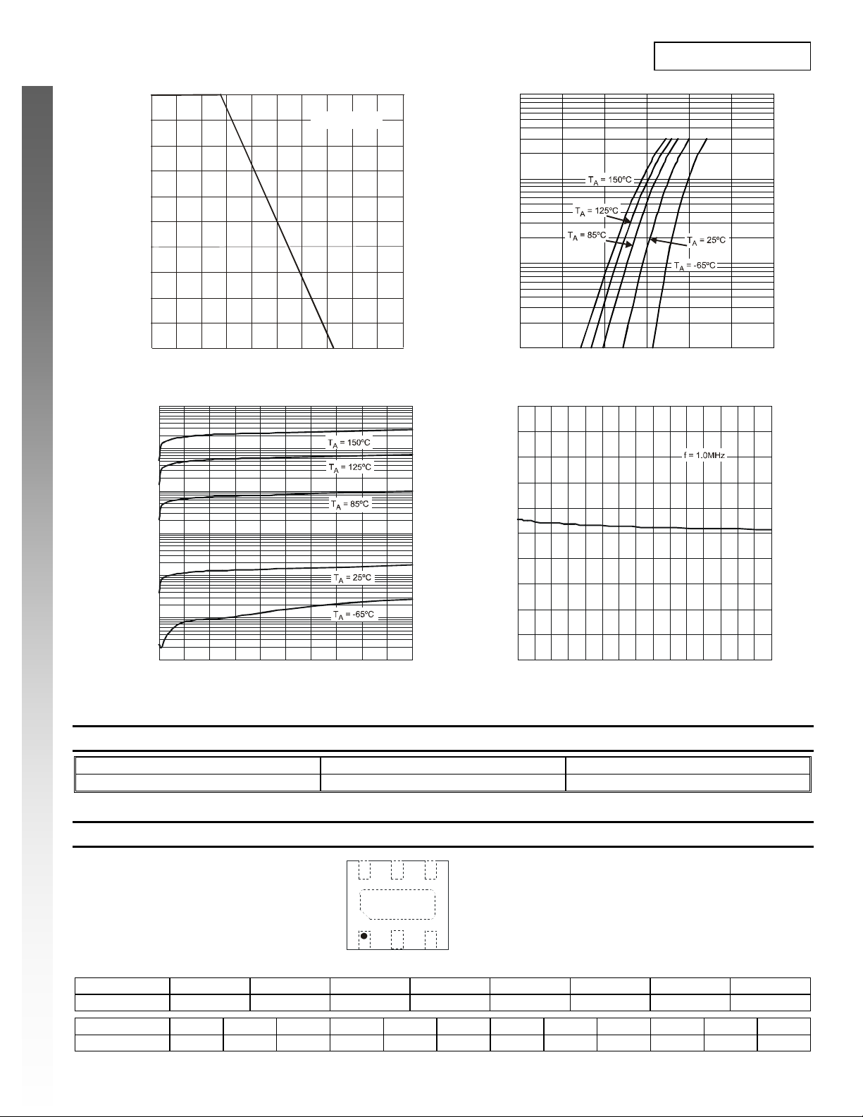
500
400
N (mW)
I
300
A
DISSI
200
D
100
0
0
NEW PRODUCT
100,000
(nA)
10,000
R = 256°C/W
θ
JA
100
T , AMBIENT TEMPERATURE, (°C)
A
Fig. 1 Power Derating Curve
200
MMBD4148PLM
1
(A)
0.1
D
S F
0.01
ANE
F
I , INS
0.001
0 500 1,000 1,500
V , INSTANTANEOUS FORWARD VOLTAGE (mV)
F
Fig. 2 Typical Forward Characteristics
2.0
1.8
1.6
E (pF)
1.4
1.2
1.0
0.8
AL
0.6
T
0.4
SE
EVE
ANE
1,000
100
10
1
0.2
R
I , INS
0
0102030405060708090100
V , INSTANTANEOUS REVERSE VOLTAGE (V)
R
Fig. 3 Typical Reverse Characteristics
0
02550
V , REVERSE VOLTAGE (V)
R
Fig. 4 Typical C apacitance vs. Reverse Voltage
75
Ordering Information (Note 5)
Part Number Case Packaging
MMBD4148PLM-7 DFN1616-6 3000/Tape & Reel
Notes: 5. For packaging details, go to our website at http://www.diodes.com/datasheets/ap02007.pdf.
Marking Information
P6 YM
Date Code Key
Year 2008 2009 2010 2011 2012 2013 2014 2015
Code V W X Y Z A B C
Month Jan Feb Mar Apr May Jun Jul Aug Sep Oct Nov Dec
Code 1 2 3 4 5 6 7 8 9 O N D
MMBD4148PLM
Document number: DS31437 Rev. 6 - 2
www.diodes.com
P6 = Product Type Marking Code
YM = Date Code Marking
Y = Year ex: V = 2008
M = Month ex: 9 = September
2 of 3
September 2008
© Diodes Incorporated
Page 3

MMBD4148PLM
Package Outline Dimensions
NEW PRODUCT
A
A1
D
e
E
E2
b
D2
A3
L
DFN1616-6
Dim Min Max Typ
A 0.545 0.605 0.575
A1 0 0.05 0.02
A3
⎯ ⎯
b 0.20 0.30 0.25
D 1.55 1.675 1.60
D2 1.10 1.30 1.20
E 1.55 1.675 1.60
e
⎯ ⎯
E2 0.30 0.50 0.40
L 0.275 0.375 0.325
All Dimensions in mm
0.13
0.50
Suggested Pad Layout
Diodes Incorporated and its subsidiaries reserve the right to make modifications, enhancements, improvements, corrections or other changes
without further notice to any product herein. Diodes Incorporated does not assume any liability arising out of the application or use of any product
described herein; neither does it convey any license under its patent rights, nor the rights of others. The user of products in such applications shall
assume all risks of such use and will agree to hold Diodes Incorporated and all the companies whose products are represented on our website,
harmless against all damages.
Diodes Incorporated products are not authorized for use as critical components in life support devices or systems without the expressed written
approval of the President of Diodes Incorporated.
Y
X2
C
Z
IMPORTANT NOTICE
LIFE SUPPORT
Dimensions Value (in mm)
Z 1.3
G 0.175
G
X1
X1 0.50
X2 0.525
Y 0.30
C 0.50
MMBD4148PLM
Document number: DS31437 Rev. 6 - 2
3 of 3
www.diodes.com
September 2008
© Diodes Incorporated
 Loading...