

Page 1
θ
θ
(
Please click here to visit our online spice models database.
Features
• Epitaxial Planar Die Construction
• High Collector-EmitterVoltage
• Ideally Suited for Automated Assembly Processes
• Ideal for Power Switching or Amplification Applications
• Lead Free By Design/RoHS Compliant (Note 1)
• "Green" Device (Note 2)
NEW PRODUCT
Maximum Ratings @T
Characteristic Symbol Value Unit
Collector-Base Voltage
Collector-Emitter Voltage
Emitter-Base Voltage
Continuous Collector Current
Peak Pulse Collector Current
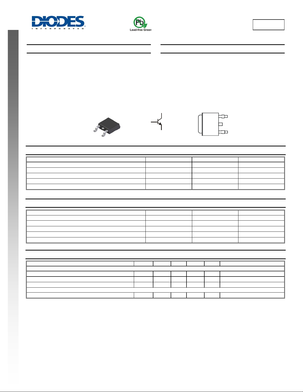
Top View
= 25°C unless otherwise specified
A
HIGH VOLTAGE NPN SURFACE MOUNT TRANSISTOR
Mechanical Data
• Case: DPAK
• Case Material: Molded Plastic, "Green" Molding Compound. UL
• Moisture Sensitivity: Level 1 per J-STD-020D
• Terminals: Finish — Matte Tin annealed over Copper Leadframe
• Marking Information: See Page 4
• Ordering Information: See Page 4
• Weight: 0.34 grams (approximate)
COLLECTOR
2,4
1
BASE
3
EMITTER
Device Schematic
MJD340
Flammability Classification Rating 94V-0
(Lead Free Plating). Solderable per MIL-STD-202, Method 208
3
24
1
Pin Out Configuration
V
CBO
V
CEO
V
EBO
I
C
I
CM
300 V
300 V
3 V
0.5 A
0.75 A
Thermal Characteristics
Characteristic Symbol Value Unit
Power Dissipation @TC = 25°C PD
Thermal Resistance, Junction to Case
Power Dissipation @TA = 25°C (Note 3) PD
Thermal Resistance, Junction to Ambient
Operating and Storage Temperature Range
Electrical Characteristics @T
OFF CHARACTERISTICS (Note 4)
Collector-Emitter Sustaining Voltage
Collector Cutoff Current
Emitter Cutoff Current
ON CHARACTERISTICS (Note 4)
DC Current Gain
Notes: 1. No purposefully added lead.
2. Diodes Inc.'s "Green" policy can be found on our website at http://www.diodes.com/products/lead_free/index.php.
3. Device mounted on FR-4 PCB with minimum recommended pad layout.
4. Measured under pulsed conditions. Pulse width = 300μs. Duty cycle ≤2%.
MJD340
Document number: DS31609 Rev. 2 - 2
Characteristic Symbol Min Typ Max Unit Test Condition
A
R
R
, T
T
J
= 25°C unless otherwise specified
V
SUS)CEO
I
CBO
I
EBO
h
FE
300
⎯ ⎯
⎯ ⎯
30
1 of 4
www.diodes.com
JC
JA
STG
⎯ ⎯
⎯
15 W
8.33 °C/W
1.56 W
80 °C/W
-55 to +150 °C
V
I
= 1mA, IB = 0
100
100
240
C
μA
μA
⎯
= 300V, IE = 0
V
CB
= 3V, IC = 0
V
EB
VCE = 10V, IC = 50mA
December 2008
© Diodes Incorporated
Page 2
C
O
CTO
R C
URR
T
C CUR
REN
T GAIN
C
O
CTO
R
T
TER
2
T
T
R
TUR
N
O
N
OLT
G
2
T
T
R
TURAT
O
N
OLT
G
NEW PRODUCT
MJD340
2.0
1.5
10
(A)
1
EN
Pw = -10ms
1.0
0.1
Pw = -100ms
DC
LLE
0.5
D
P , POWER DISSIPATI ON (W)
1,000
R = 81°C/W
θ
JA
0
25 50 75 100 125 150
0
T , AMBIENT TEMPERA TURE ( C)
A
°
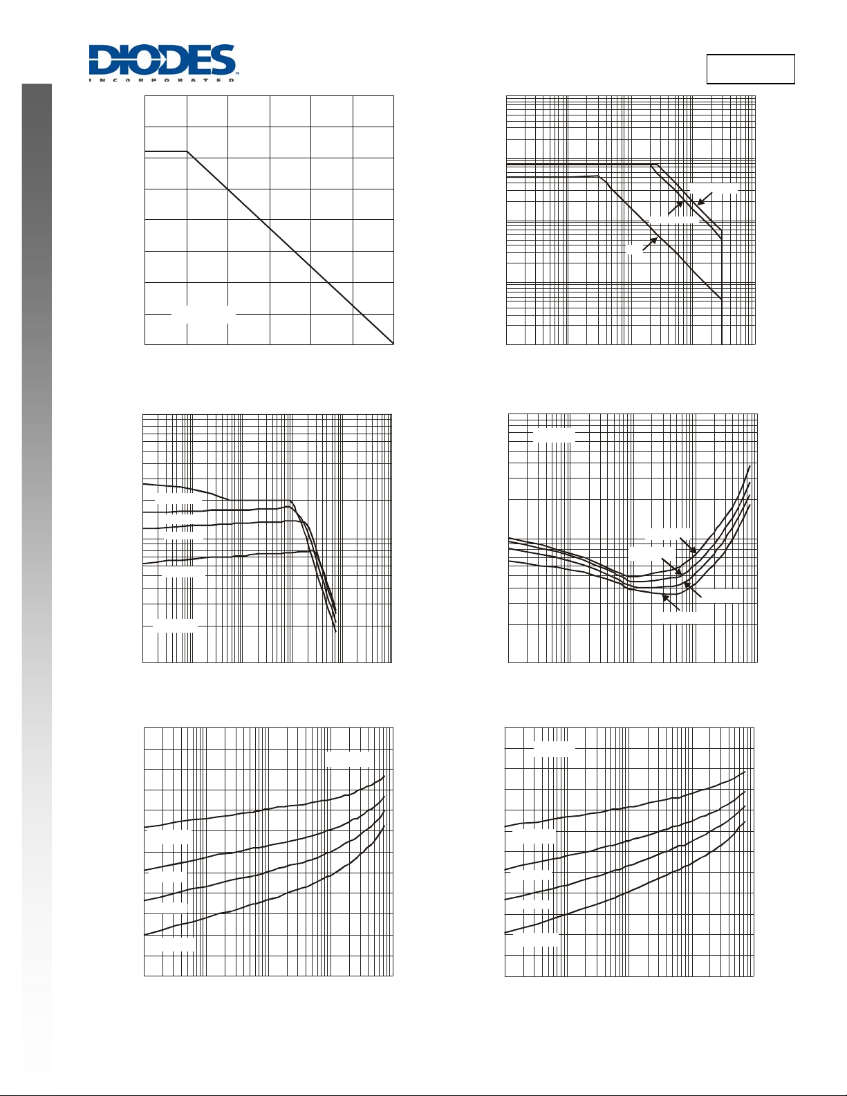
Fig. 1 Pow er D issipati o n
vs. Ambient Temperat ur e (Note 3)
0.01
C
I,
0.001
0.1 1 10 100 1,000
V , COLLECTOR-EMITTER VOLTAGE (V)
CE
Fig. 2 Typical Collector Current
vs. Collector-Emitter Voltage (Note 3)
1
I/I = 10
CB
T = 150°C
A
T = 85°C
A
T = 25°C
100
FE
h, D
A
T = -55°C
A
V = 2V
CE
10
0.1 1 10 100 1,000 10,000
I , COLLECTOR CURRENT (mA)
Fig. 3 Typical DC Current Gain vs. Collector Current
C
1.
E (V)
A
1.0
V = 2V
CE
V
0.8
-
T = -55°C
A
0.6
E
T = 25°C
A
0.4
T = 85°C
A
-EMI
VOLTAGE (V)
0.1
LLE
SATURATION
CE(SAT)
V,
T = 150°C
A
T = 85°C
A
T = -55°C
A
T = 25°C
A
0.01
0.1 1 10 100 1,000
I , COLLECTOR CURRENT (mA)
Fig. 4 Typical Collector-Emitter Saturation Voltage
C
vs. Collecto r Cu r re nt
1.
I = 10
/I
E (V)
A
1.0
CB
V
0.8
I
T = -55°C
A
0.6
SA
T = 25°C
A
E
0.4
T = 85°C
A
0.2
T = 150°C
A
BE(ON)
0
V, BASE-EMI
0.1 1 10 100 1,000
I , COLLECTOR CURRENT (mA)
C
Fig. 5 Typical Base-Emitter Turn-On Voltage
vs. Collector Current
0.2
T = 150°C
A
0
0.1 1 10 100 1,000
BE(SAT)
V , BASE-EMI
I , COLLECTOR CURRENT (mA)
C
Fig. 6 Typical Base-Emitter Saturation Voltage
vs. Collector Current
MJD340
Document number: DS31609 Rev. 2 - 2
2 of 4
www.diodes.com
December 2008
© Diodes Incorporated
Page 3

CAPACITAN
C
F
T
R
T T
HER
R
TANC
Y
NEW PRODUCT
MJD340
1,000
)
100
f = 1MHz
C
ibo
E (p
10
C
obo
1
0.1 1 10 100
V , REVERSE VOLTAGE (V)
R
Fig. 7 Typical Capacitance Characteristics
1
D = 0.7
E
D = 0.5
D = 0.3
ESIS
0.1
D = 0.1
MAL
0.01
ANSIEN
r(t),
D = 0.05
D = 0.02
D = 0.01
D = 0.005
D = Single Pulse
D = 0.9
R (t) = r(t) *
θ
JA
R = 81°C/W
JA
P(pk)
t
1
t
2
T - T = P * R (t)
JA JA12θ
Duty Cycle, D = t /t
R
θθJA
0.001
0.00001 0.0001 0.001 0.01 0.1 1 10 100 1,000
t , PULSE DURATION TIME (s)
1
Fig. 8 Transient Thermal Response (Note 3)
Ordering Information (Note 5)
Part Number Case Packaging
MJD340-13 DPAK 2500/Tape & Reel
Notes: 5. For packaging details, go to our website at http://www.diodes.com/datasheets/ap02007.pdf.
Marking Information
YWW
MJD340
MJD340
Document number: DS31609 Rev. 2 - 2
www.diodes.com
MJD340 = Product Type Marking Code
= Manufacturers’ code marking
YYWW = Date Code Marking
YY = Last Digit of Year (ex: 08 = 2008)
WW = Week Code 01-52
3 of 4
December 2008
© Diodes Incorporated
Page 4

Package Outline Dimensions
NEW PRODUCT
b
E
b2
e
e
1
L2
D
L1
A1
L
C
H
SEATING
PLANE
A
C1
All Dimensions in mm
DPAK
Dim Min Max
A 2.18 2.40
A1 0.89 1.14
b 0.61 Typ
b2 5.20 5.50
C 0.45 0.58
C1 0.45 0.58
D 5.40 6.20
E 6.35 6.80
e 2.28 Typ
e1 4.57 Typ
H 9.00 10.40
L 0.51
L1 0.64 1.02
L2 0.88 1.27
⎯
Suggested Pad Layout
Diodes Incorporated and its subsidiaries reserve the right to make modifications, enhancements, improvements, corrections or other changes
without further notice to any product herein. Diodes Incorporated does not assume any liability arising out of the application or use of any product
described herein; neither does it convey any license under its patent rights, nor the rights of others. The user of products in such applications shall
assume all risks of such use and will agree to hold Diodes Incorporated and all the companies whose products are represented on our website,
harmless against all damages.
Diodes Incorporated products are not authorized for use as critical components in life support devices or systems without the expressed written
approval of the President of Diodes Incorporated.
X2
Y2
Z
C
E1
X1
Y1
IMPORTANT NOTICE
LIFE SUPPORT
Dimensions Value (in mm)
Z 11.6
X1 1.5
X2 7.0
Y1 2.5
Y2 7.0
C 6.9
E1 2.3
MJD340
MJD340
Document number: DS31609 Rev. 2 - 2
4 of 4
www.diodes.com
December 2008
© Diodes Incorporated
 Loading...