DIODES MBRB1540CT, MBRB1545CT, MBRB1535CT, MBRB1530CT Datasheet

MBRB1530CT - MBRB1545CT
15A SURFACE MOUNT SCHOTTKY BARRIER RECTIFIER
Features
Schottky Barrier Chip
·
Guard Ring Die Construction for
·
Transient Protection
Low Power Loss, High Efficiency
·
High Surge Capability
·
High Current Capability and Low Forward
·
Voltage Drop
Surge Overload Rating to 150A Peak
·
For Use in Low Voltage, High Frequency
·
Inverters, Free Wheeling, and Polarity
Protection Applications
Plastic Material - UL Flammability
·
Classification 94V-0
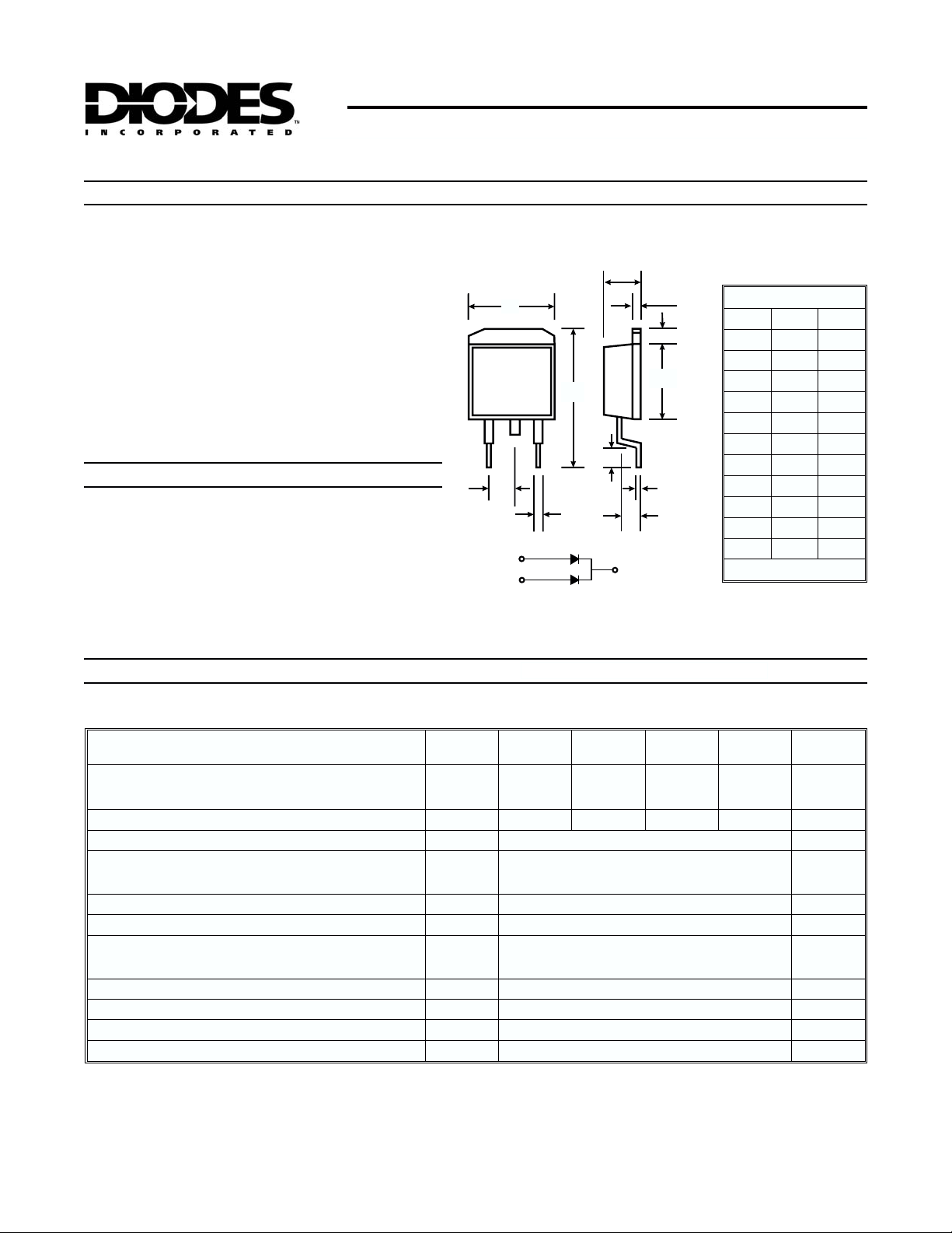
Mechanical Data
2
· Case: D
· Terminals: Solderable per MIL-STD-202,
Method 208
· Polarity: See Diagram
· Approx. Weight: 1.7 grams
· Mounting Position: Any
· Marking: Type Number
PAK Molded Plastic
A
4
123
D
PIN 1
PIN 3
E
G
H
J
B
M
K
C
L
PIN2&4
D2PAK
A
B
C
D
E
G
H
J
K
L
M
Min Max
9.65 10.69
14.60 15.88
0.51 1.14
2.29 2.79
4.37 4.83
1.14 1.40
1.14 1.40
8.25 9.25
0.30 0.64
2.03 2.92
2.29 2.79
Dim
All Dimensions in mm
Maximum Ratings and Electrical Characteristics
Single phase, half wave, 60Hz, resistive or inductive load.
For capacitive load, derate current by 20%.
Characteristic Symbol
Peak Repetitive Reverse Voltage
Working Peak Reverse Voltage
DC Blocking Voltage
RMS Reverse Voltage
Average Rectified Output Current @ TC= 105°C
Non-Repetitive Peak Forward Surge Current 8.3ms
single half sine-wave superimposed on rated load
(JEDEC Method)
Forward Voltage, per Element (Note 4) @ IF= 7.5A
Voltage Rate of Change
Peak Reverse Current @TA= 25°C
at Rated DC Blocking Voltage @ T
Maximum Recovery Time (Note 3)
Typical Junction Capacitance (Note 2)
Typical Thermal Resistance Junction to Terminal (Note 1)
Operating and Storage Temperature Range
Notes: 1. Thermal resistance: junction to terminal, unit mounted on PC board with 5.0 mm2(0.013 mm thick) copper pad as heat sink.
2. Measured at 1.0 MHz and applied reverse voltage of 4.0V DC.
3. Reverse recovery test conditions: I
4. 300µs pulse width, 2% duty cycle.
= 100°C
A
= 0.5A, IR= 1.0A, Irr= 0.25A (see figure 1).
F
V
RRM
V
RWM
V
R
V
R(RMS)
I
O
I
FSM
V
FM
dv/dt 10,000 V/µs
I
RM
t
rr
C
j
R
qJT
T
j,TSTG
@ TA= 25°C unless otherwise specified
MBRB
1530CT
30 35 40 45 V
21 24.5 28 31.5 V
MBRB
1535CT
-65 to +150 °C
MBRB
1540CT
15 A
150 A
0.7 V
0.1
15
30 ns
250 pF
3.0 K/W
MBRB
1545CT
Unit
mA
DS13015 Rev. B-2 1 of 2 MBRB1530CT-MBRB1545CT

300
g
100
g
16
20
g
100
g
1000
g
12
8
4
(AV)
I , AVERAGE FORWARD CURRENT (A)
0
0 50 100 150
T , CASE TEMPERATURE (°C)
C
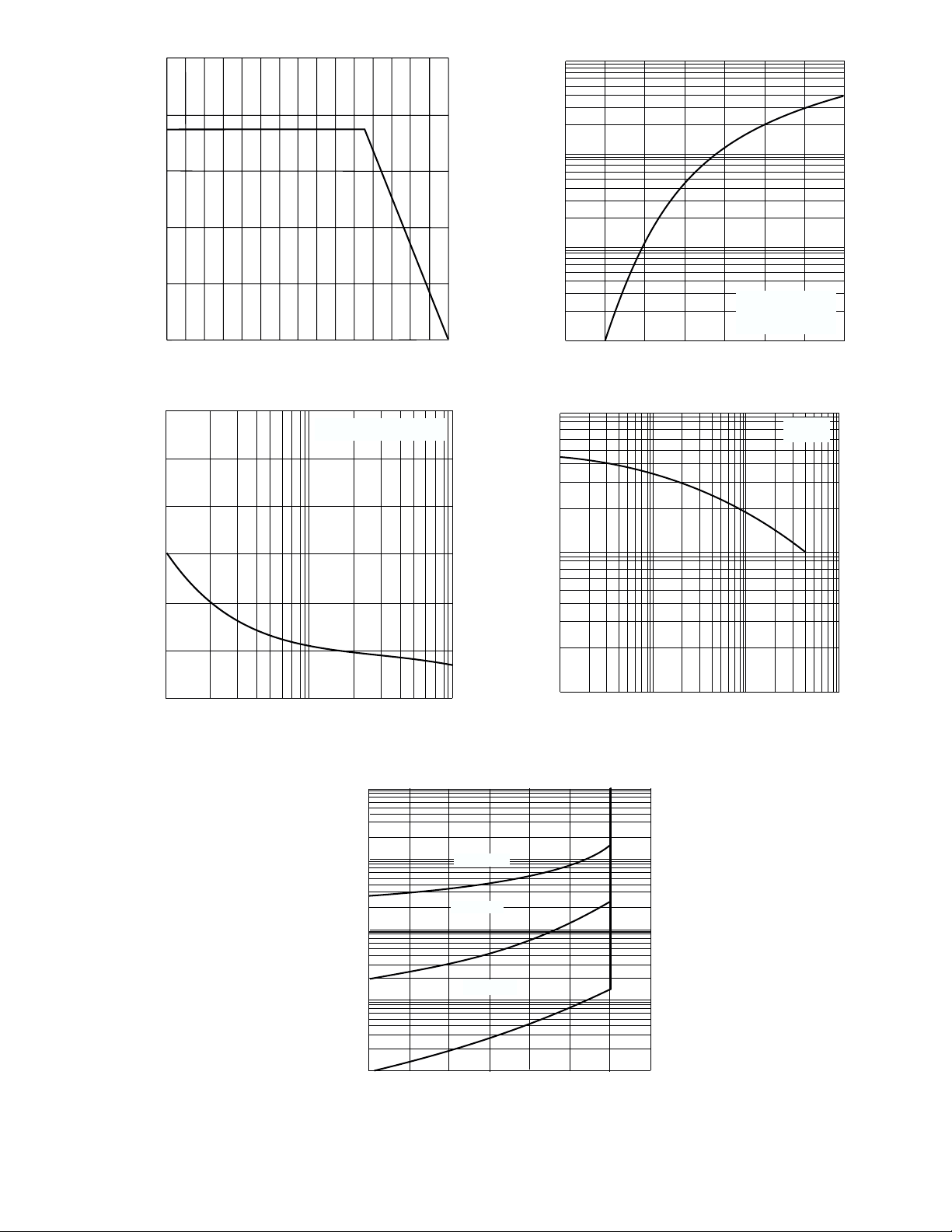
. 1 Fwd Current DeratingCurve
Fi
10
1.0
F
I , INSTANTANEOUS FORWARD CURRENT (A)
0.1
0.2 0.4 0.6 0.8
V , INSTANTANEOUS FORWARD VOLTAGE (V)
F
Fi
.2 Typical Fwd Characteristics per Element
T = 25°C
j
Pulse width = 300 µs
2% duty cycle
FSM
I , PEAK FORWARD SURGE CURRENT (A)
250
200
150
100
50
8.3 ms single half-sine-wave
JEDEC method
T = 25°C
j
f = 1MHz
100
j
C , JUNCTION CAPACITANCE (pF)
0
1
10
100
NUMBER OF CYCLES AT 60 Hz
. 3 Max Non-Repetitive Surge Current
Fi
10
T = 100°C
j
10
0.1 1.0 10 100
V , REVERSE VOLTAGE (V)
R
.4 Typical Junction Capacitance
Fi
T = 75°C
j
1.0
T = 25°C
40
j
80 120
R
I , INSTANTANEOUS REVERSE CURRENT (mA)
0.01
0.1
0
PERCENT OF RATED PEAK REVERSE VOLTAGE (%)
.5 Typical Reverse Characteristics, per element
Fi
DS13015 Rev. B-2 2 of 2 MBRB1530CT-MBRB1545CT
 Loading...