

Page 1
Features and Benefits
• Guard Ring Die Construction for Transient Protection
• Low Power Loss, High Efficiency
• High Surge Capability
• High Current Capability and Low Forward Voltage Drop
• Surge Overload Rating to 150A Peak
• For Use in Low Voltage, High Frequency Inverters, Free
Wheeling, and Polarity Protection Applications
• Lead Free Finish, RoHS Compliant (Note 1)
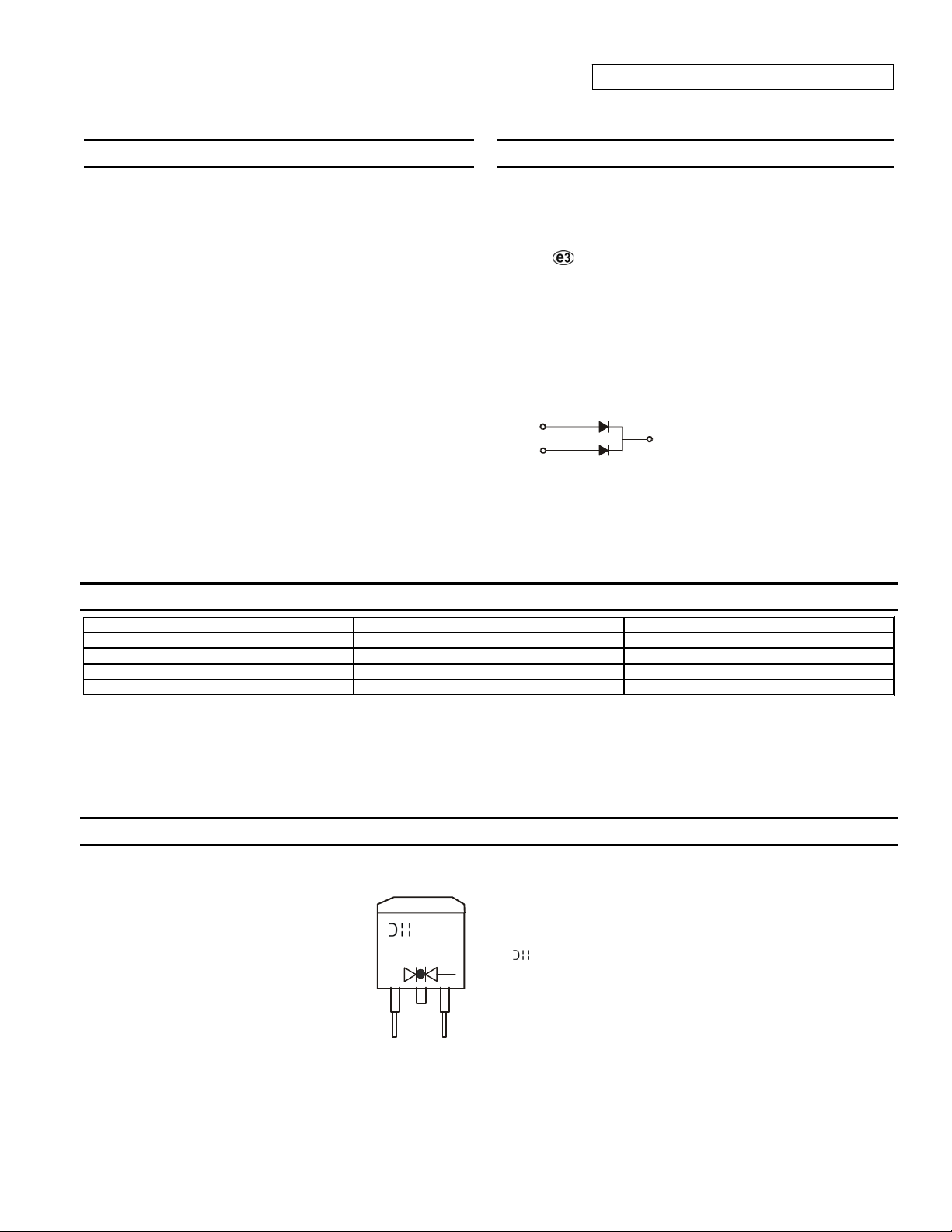
Top View
MBRB1530CT - MBRB1545CT
15A SURFACE MOUNT SCHOTTKY BARRIER RECTIFIER
Mechanical Data
• Case: D2PAK
• Case Material: Molded Plastic. UL Flammability Classification
Rating 94V-0
• Moisture Sensitivity: Level 1 per J-STD-020
• Terminals: Finish ⎯ Tin. Solderable per MIL-STD-202, Method
208
• Polarity: See Diagram
• Weight: 1.7 grams (approximate)
PIN 1
PIN 3
Polarity
PIN 2 & 4
Ordering Information (Note 2)
Device Packaging Shipping
MBRB1530CT-T D2PAK 800/Tape & Reel, 13-inch
MBRB1535CT-T D2PAK 800/Tape & Reel, 13-inch
MBRB1540CT-T D2PAK 800/Tape & Reel, 13-inch
MBRB1545CT-T D2PAK 800/Tape & Reel, 13-inch
Notes: 1. EU Directive 2002/95/EC (RoHS). All applicable RoHS exemptions applied, see EU Directive 2002/95/EC Annex Notes
2. For packaging details, visit our website at http://www.diodes.com/datasheets/ap02007.pdf.
Marking Information
MBRB1530CT - MBRB1545CT
Document number: DS13015 Rev. 7 - 2
YWW
MBRB15XXCT
www.diodes.com
MBRB15XXCT = Product Type Marking Code Where
xx = 30, 35, 40 or 45, Depending on Device Type
= Manufacturers’ Code Marking
YWW = Date Code Marking
Y = Last Digit of Year (ex: 2 for 2002)
WW = Week Code (01 to 53)
1 of 4
May 2011
© Diodes Incorporated
Page 2
)
V
r
R
G
F
O
R
R
C
URR
T
NSTAN
TAN
O
US F
O
R
R
C
URREN
T
Maximum Ratings @T
= 25°C unless otherwise specified
A
Single phase, half wave, 60Hz, resistive or inductive load.
For capacitive load, derate current by 20%.
Characteristic Symbol
Peak Repetitive Reverse Voltage
Working Peak Reverse Voltage
V
V
DC Blocking Voltage
RMS Reverse Voltage
V
R(RMS
Average Rectified Output Current @ TC = 105°C IO
Non-Repetitive Peak Forward Surge Current 8.3ms
Single Half Sine-Wave Superimposed on Rated Load
I
Thermal Characteristics
Characteristic Symbol
Typical Thermal Resistance Junction to Terminal
V
Operating Temperature Range (Note 3)
Storage Temperature Range
≤ 80% V
R
VR ≤ 50% V
DC Forward Mode ≤200
RRM
RRM
RRM
RWM
V
R
FSM
MBRB1530CT - MBRB1545CT
MBRB
1530CT
30 35 40 45 V
21 24.5 28 31.5 V
R
JT
θ
T
J
T
STG
MBRB
1535CT
MBRB
1540CT
1545CT
15 A
150 A
alue Unit
3.0 °C/W
-65 to +150
≤180
-65 to +175 °C
MBRB
Unit
°C
Electrical Characteristics @T
= 25°C unless otherwise specified
A
Characteristic Symbol Value Unit
Forward Voltage, per Element @ IF = 7.5A VFM
0.7 V
Voltage Rate of Change dv/dt 10,000 V/µs
Peak Reverse Current @ TA = 25°C
at Rated DC Blocking Voltage (Note 4) @ T
= 100°C
A
Maximum Reverse Recovery Time (Note 5)
Typical Total Capacitance (Note 6)
Notes: 3. The heat generated must be less than the thermal conductivity from Junction-to-Ambient: dPD/dTJ < 1/R
4. 300µs pulse width, 2% duty cycle.
5. Reverse recovery test conditions: IF = 0.5A, IR = 1.0A, Irr = 0.25A (see figure 1).
6. Measured at 1.0 MHz and applied reverse voltage of 4.0V DC.
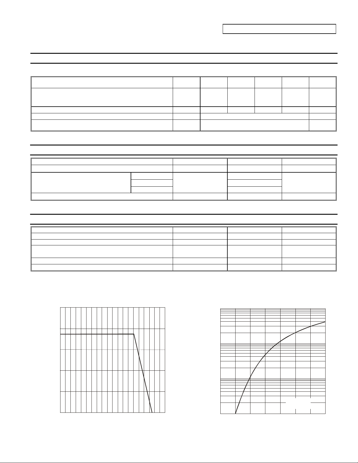
20
I
RM
t
r
C
T
100
0.1
15
mA
30 ns
250 pF
θJA
(A)
(A)
16
EN
10
12
D
D
WA
WA
8
E
A
1.0
E
4
(AV)
I, AVE
0
050100 200
T , CASE TEMPERATURE (°C)
C
Fig. 1 Forward Current Derating Curve
MBRB1530CT - MBRB1545CT
Document number: DS13015 Rev. 7 - 2
150
2 of 4
www.diodes.com
F
I, I
0.1
0.2 0.4 0.6 0.8
V , INSTANTANEOUS FORWARD VOLTAGE (V)
F
Fig. 2 Typical Forward Character istics, per El ement
ο
T = 25C
j
© Diodes Incorporated
May 2011
Page 3

P
FORWAR
U
R
G
CUR
RENT
C, TOT
CAPACITANC
F
NSTAN
TANEO
US R
R
CUR
REN
T
300
8.3 ms single half-sine-wave
1,000
(A)
E
D S
EAK
FSM
I,
250
200
150
100
50
0
1
NUMBER OF CYCLES AT 60 Hz
10
Fig. 3 Max Non-Repetitive Surge Current
100
)
E (p
100
AL
T
10
100
MBRB1530CT - MBRB1545CT
T = 25°C
j
f = 1MHz
0.1 1.0 10 100
V , DC REVERSE VOLTAGE (V)
R
Fig. 4 Typical Total Ca pacitance
(mA)
10
SE
1.0
EVE
0.1
R
I, I
0.01
0
40 80 120
PERCENT OF RATED PEAK REVERSE VOLTAGE (%)
Fig. 5 Typical Reverse Char acteris t ics, per el em ent
Package Outline Dimensions
E
12K
e
MBRB1530CT - MBRB1545CT
Document number: DS13015 Rev. 7 - 2
b1
L1
D2PAK
Dim Min Max
D
H
A 4.07 4.82
b 0.51 0.99
b1 1.15 1.77
c 0.356 0.58
L2
c1 1.143 1.65
D 8.39 9.65
E 9.66 10.66
b
c
A
a
L
c1
3 of 4
www.diodes.com
e 2.54 Typ
H 14.61 15.87
L 1.78 2.79
L1
L2
⎯
⎯
1.67
1.77
a 0° 8°
All Dimensions in mm
May 2011
© Diodes Incorporated
Page 4

MBRB1530CT - MBRB1545CT
Suggested Pad Layout
DIODES INCORPORATED MAKES NO WARRANTY OF ANY KIND, EXPRESS OR IMPLIED, WITH REGARDS TO THIS DOCUMENT,
INCLUDING, BUT NOT LIMITED TO, THE IMPLIED WARRANTIES OF MERCHANTABILITY AND FITNESS FOR A PARTICULAR PURPOSE
(AND THEIR EQUIVALENTS UNDER THE LAWS OF ANY JURISDICTION).
Diodes Incorporated and its subsidiaries reserve the right to make modifications, enhancements, improvements, corrections or other changes
without further notice to this document and any product described herein. Diodes Incorporated does not assume any liability arising out of the
application or use of this document or any product described herein; neither does Diodes Incorporated convey any license under its patent or
trademark rights, nor the rights of others. Any Customer or user of this document or products described herein in such applications shall assume
all risks of such use and will agree to hold Diodes Incorporated and all the companies whose products are represented on Diodes Incorporated
website, harmless against all damages.
Diodes Incorporated does not warrant or accept any liability whatsoever in respect of any products purchased through unauthorized sales channel.
Should Customers purchase or use Diodes Incorporated products for any unintended or unauthorize d application, Customers shall indemnify and
hold Diodes Incorporated and its representatives harmless against all claims, damages, expenses, and attorney fees arising out of, directly or
indirectly, any claim of personal injury or death associated with such unintended or unauthorized application.
Products described herein may be covered by one or more United States, international or foreign patents pending. Product names and markings
noted herein may also be covered by one or more United States, international or foreign trademarks.
Diodes Incorporated products are specifically not authorized for use as critical components in life support devices or systems without the express
written approval of the Chief Executive Officer of Diodes Incorporated. As used herein:
A. Life support devices or systems are devices or systems which:
1. are intended to implant into the body, or
2. support or sustain life and whose failure to perform when properly used in accordance with instructions for use provided in the
labeling can be reasonably expected to result in significant injury to the user.
B. A critical component is any component in a life support device or system whose failure to perform can be reasonably expected to cause the
failure of the life support device or to affect its safety or effectiveness.
Customers represent that they have all necessary expertise in the safety and regulatory ramifications of their life support devices or systems, and
acknowledge and agree that they are solely responsible for all legal, regulatory and safety-related requirements concerning their products and any
use of Diodes Incorporated products in such safety-critical, life support devices or systems, notwithstanding any devices- or systems-related
information or support that may be provided by Diodes Incorporated. Further, Customers must fully indemnify Diodes Incorporated and its
representatives against any damages arising out of the use of Diodes Incorporated products in such safety-critical, life support devices or systems.
Copyright © 2011, Diodes Incorporated
www.diodes.com
Y2
Y1
X1
X2
E1
Z
C
IMPORTANT NOTICE
LIFE SUPPORT
Dimensions Value (in mm)
Z 16.9
X1 1.1
X2 10.8
Y1 3.5
Y2 11.4
C 9.5
E1 2.5
MBRB1530CT - MBRB1545CT
Document number: DS13015 Rev. 7 - 2
4 of 4
www.diodes.com
May 2011
© Diodes Incorporated
 Loading...