Diodes MBR5H150 User Manual

HIGH VOLTAGE POWER SCHOTTKY RECTIFIER MBR5H150
Preliminary Datasheet
General Description
High voltage schottky rectifier suited for switch
mode power supplies and other power converters.
This device is intended for use in medium voltage
operation, and particularly, in high frequency circuits
where low switching losses and low noise are
required.
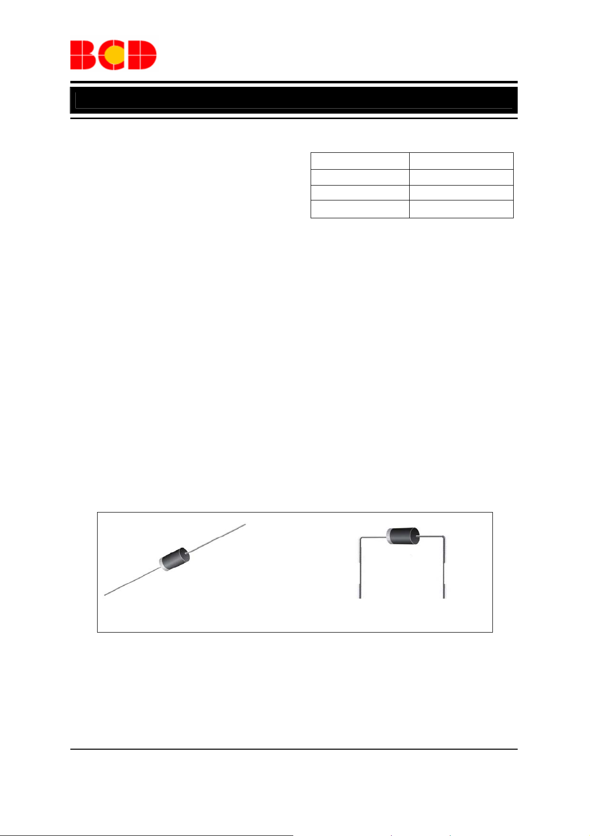
The MBR5H150 is available in standard DO-27 and
DO-27(A) packages.
Main Product Characteristics
I
5A
F(AV)
V
150V
RRM
TJ
V
0.92V
F(max)
175°C
Features
High Surge Capacity
•
• Low Forward Voltage Drop
• 175°C Operating Junction Temperature
• Guard-Ring for Stress Protection
• Pb-Free and Halogen-Free Packages are
available
• The Plastic Material Carries UL Recongnition
94V-0
Mechanical Characteristics
• Case: JEDEC DO-201AD Molded Plastic
• Epoxy Meets UL 94 V-0@ 0.125 in
• Weight (Approximately): 1.2 Grams
• Finish: All External Surfaces Corrosion
Resistant and Terminal
Applications
• Power Supply − Output Rectification
• Power Management
• Instrumentation
DO-27 DO-27(A)
Figure 1. Package Type of MBR5H150
Aug. 2009 Rev. 1. 0 BCD Semiconductor Manufacturing Limited
1

Preliminary Datasheet
HIGH VOLTAGE POWER SCHOTTKY RECTIFIER MBR5H150
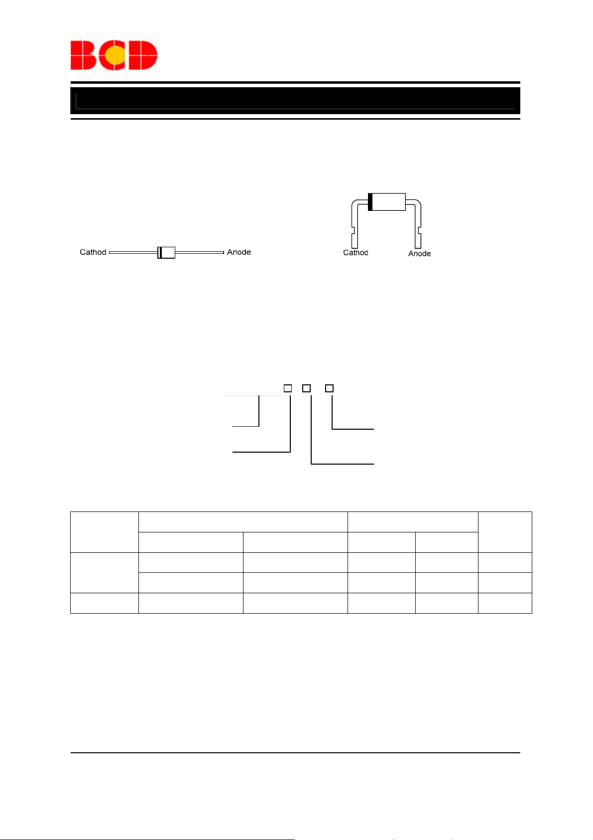
Pin Configuration
VP Pacakge VPA Package
(DO-27) (DO-27(A))
Figure 2. Pin Configuration of MBR5H150 (Top View)
Ordering Information
MBR5H150 -
Circuit Type E1: Lead Free
G1: Green
Package
VP: DO-27
VPA: DO-27(A) TR: Ammo
Part Number Marking ID
Package
Lead Free Green Lead Free Green
Blank: Tube
Packing
Type
DO-27
DO-27(A) MBR5H150VPA-E1 MBR5H150VPA-G1 515VP 515VPG Bulk
MBR5H150VP-E1 MBR5H150VP-G1 515VP 515VPG Bulk
MBR5H150VPTR-E1 MBR5H150VPTR-G1 515VP 515VPG Ammo
BCD Semiconductor's Pb-free products, as designated with "E1" suffix in the part number, are RoHS compliant.
Products with “G1” suffix are available in green packages.
Aug. 2009 Rev. 1. 0 BCD Semiconductor Manufacturing Limited
2

Preliminary Datasheet
HIGH VOLTAGE POWER SCHOTTKY RECTIFIER MBR5H150
Absolute Maximum Ratings ( Per Diode Leg) (Note 1)
Parameter Symbol Value Unit
V
Peak Repetitive Reverse Voltage
Working Peak Reverse Voltage
DC Blocking Voltage
Average Rectified Forward Current
(Rated V
Non repetitive Peak Surge Current
(Surge applied at rated load conditions half wave, single phase, 60Hz)
Operating Junction Temperature Range(Note 2)
) TC = 150°C
R
RRM
V
RWM
V
R
I
5 A
F(AV)
I
125 A
FSM
TJ 175
150 V
°C
Storage Temperature Range
Voltage Rate of Change (Rated VR)
ESD Ratings: Machine Model = C
Human Body Model =3B
Note 1: Stresses greater than those listed under “Absolute Maximum Ratings” may cause permanent damage to
the device. These are stress ratings only, and functional operation of the device at these or any other conditions
beyond those indicated under “Recommended Operating Conditions” is not implied. Exposure to “Absolute
Maximum Ratings” for extended periods may affect device reliability.
Note 2: The heat generated must be less than the thermal conductivity from Junction−to−Ambient: dP
.
1/θ
JA
T
-55 to 175
STG
dv/dt 10000
> 400
> 8000
D
°C
V/µs
V
/dTJ <
Recommended Operating Conditions
Parameter Symbol Condition Value Unit
Junction to Case TBD
Junction to
Ambient
TBD
°C/W
Maximum Thermal Resistance
θJC
θ
JA
Electrical Characteristics
Parameter Symbol Conditions Value
Maximum Instantaneous Forward
Voltage Drop (Note 3)
VF
IF=5A, TC=25°C
0.92 V
Units
Maximum Instantaneous Reverse
Current (Note 3)
IR
Rated DC Voltage,
T
=25°C
C
Rated DC Voltage,
T
=150°C
C
8.0
50.0
µA
mA
Note 3: Pulse Test: Pulse Width = 300µs, Duty Cycle ≤2.0%.
Aug. 2009 Rev. 1. 0 BCD Semiconductor Manufacturing Limited
3
 Loading...