Diodes LMV393 User Manual

LMV331/ LMV393
GENERAL PURPOSE LOW VOLTAGE COMPARATOR
Description
The LMV331/LMV393 series are low voltage (2.7V to 5.5V) single
and dual comparators, which are designed to effectively reduce cost
and space at low voltage levels.
These devices offer specifications that meet or exceed the familiar
LM331/LM393 devices operating with a lower supply voltage and
consuming a far lower supply current.
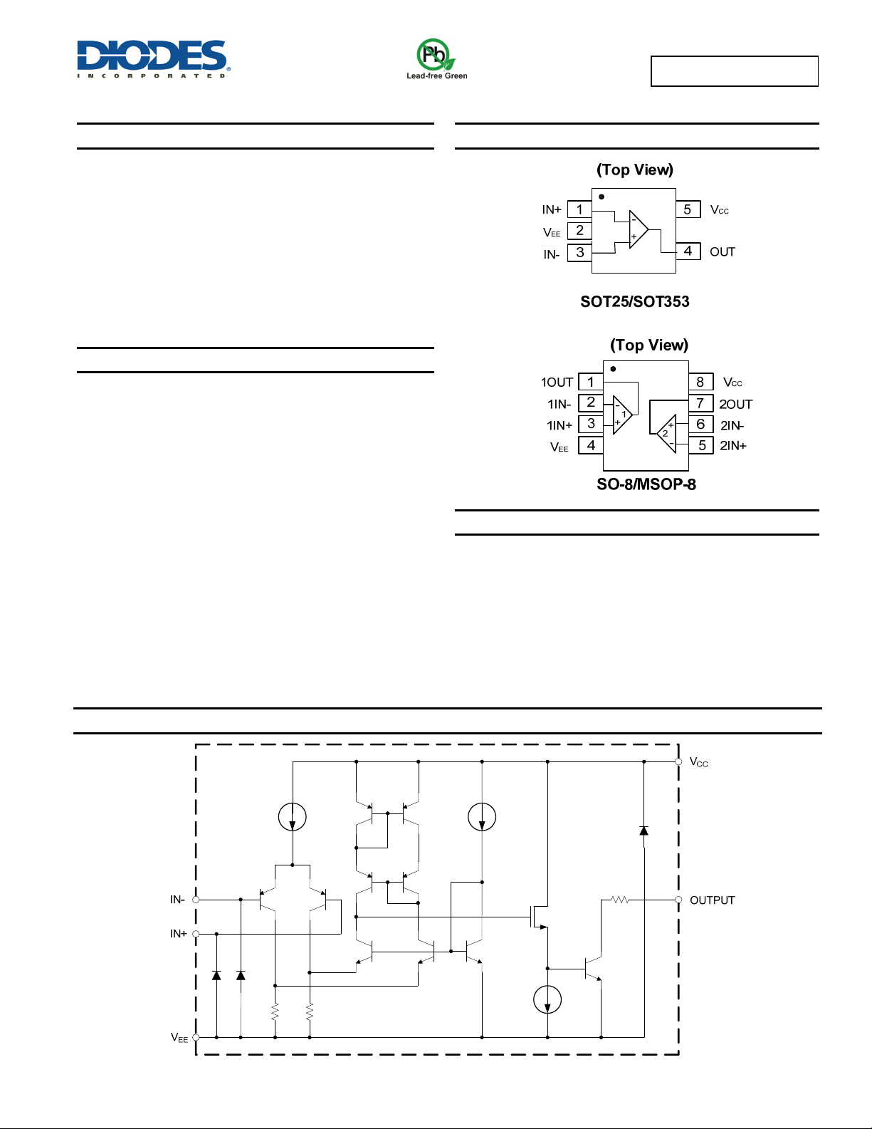
The LMV331 is available in 5-Pin SOT353/SOT25 packages that
reduce space on PC boards and portable electronic devices. LMV393
is available in industry standard SOP-8 and MSOP-8 packages.
Pin Assignments
Features
• Guaranteed 2.7V and 5.5V performance
• Operating temperature range (-40°C to +125°C)
• Low supply current 40 µA/comparator Typ
• Input Common Mode Voltage Range includes ground
• Open Collector Output for Maximums Flexibility
• SOT353, SOT25, MSOP-8, SO-8: Available in “Green” Molding
ADVANCED INFORMATION
Compound (No Br, Sb)
• Totally Lead-Free & Fully RoHS Compliant (Notes 1 & 2)
• Halogen and Antimony Free. “Green” Device (Note 3)
Notes: 1. No purposely added lead. Fully EU Directive 2002/95/EC (RoHS) & 2011/65/EU (RoHS 2) compliant.
2. See http://www.diodes.com/quality/lead_free.html for more information about Diodes Incorporated’s definitions of Halogen- and Antimony-free, "Green"
and Lead-free.
3. Halogen- and Antimony-free "Green” products are defined as those which contain <900ppm bromine, <900ppm chlorine (<1500ppm total Br + Cl) and
<1000ppm antimony compounds.
Applications
• Mobile communications
• Battery powered devices
• Notebooks and PDA’s
• General purpose low voltage applications
• General purpose portable devices
Schematic Diagram
LMV331/ LMV393
Document number: DS37022 Rev. 1 - 2
Each Comparator
1 of 13
www.diodes.com
May 2014
© Diodes Incorporated

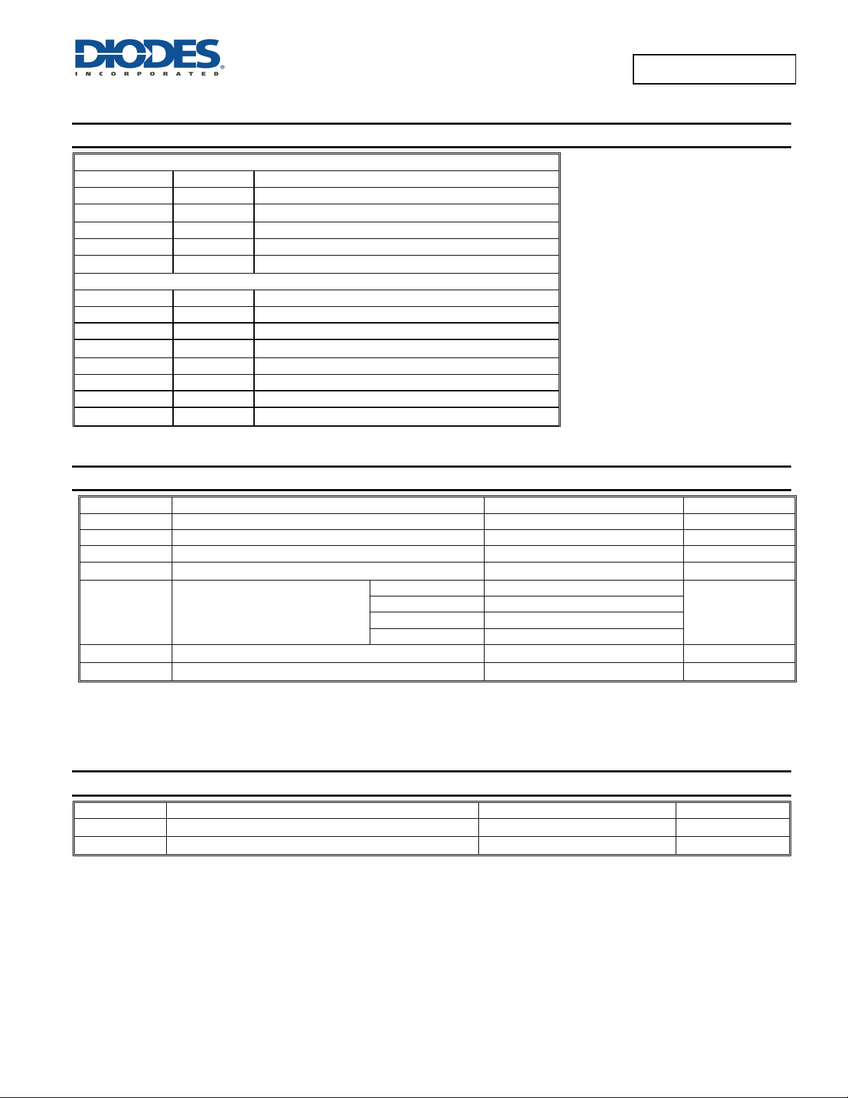
Pin Descriptions
LMV331
Pin Name Pin # Function
IN+ 1 Non-inverting Input
VEE
IN- 3 Inverting Input
OUT 4 Output
VCC
LMV393
1OUT 1 Channel 1 Output
1IN- 2 Channel 1 Inverting Input
1IN+ 3 Channel 1 Non-inverting Input
VEE
2IN+ 5 Channel 2 Non-inverting Input
2IN- 6 Channel 2 Inverting Input
2OUT 7 Channel 2 Output
VCC
ADVANCED INFORMATION
Absolute Maximum Ratings (Note 4) (@T
Symbol Description Rating Unit
ESD HBM Human Body Model ESD Protection 4.0 KV
ESD MM Machine Model ESD Protection 300 V
Differential Input Voltage ±Supply Voltage V
θJA
TST
TJ
EE
VCC -V
Notes: 4. Stresses greater than the 'Absolute Maximum Ratings' specified above, may cause permanent damage to the device. These are stress ratings only;
functional operation of the device at these or any other conditions exceeding those indicated in this specification is not implied. Device reliability may be
affected by exposure to absolute maximum rating conditions for extended periods of time.
5. All numbers are typical, and apply for packages soldered directly onto a PC board in still air.
2 Chip Supply Voltage(Negative)/GND
5 Chip Supply Voltage(Positive)
4 Chip Supply Voltage(Negative)/GND
8 Chip Supply Voltage(Positive)
Supply Voltage 5.5 V
Thermal Resistance Junction-toAmbient
Storage Temperature -65 to 150 °C
Maximum Junction Temperature 150 °C
Recommended Operating Conditions (@T
Symbol Description Rating Unit
VCC -VEE
TA
Supply Voltage 2.7 to 5.5 V
Operating Ambient Temperature Range
LMV331/ LMV393
Document number: DS37022 Rev. 1 - 2
= +25°C, unless otherwise specified.)
A
SOT353 (Note 5) TBD
SOT25 (Note 5) TBD
SO-8 (Note 5) TBD
MSOP-8 (Note 5) TBD
= +25°C, unless otherwise specified.)
A
-40 to +125
2 of 13
www.diodes.com
LMV331/ LMV393
°C/W
°C
May 2014
© Diodes Incorporated

LMV331/ LMV393
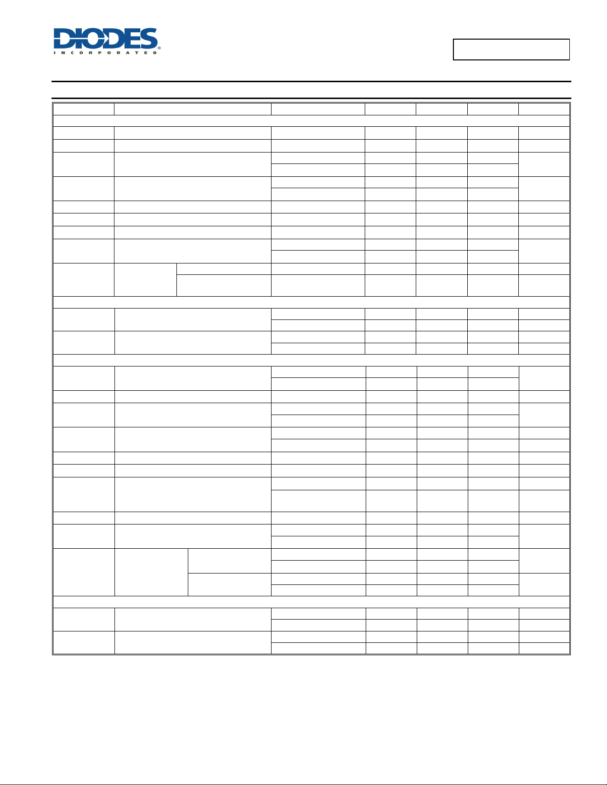
Electrical Characteristics (Notes 6 & 7) (@T
= +25°C, VEE = 0V, VCM = 0V and RL = 5.1KΩ, unless otherwise specified.)
A
Symbol Parameter Test Conditions Min Typ Max Unit
2.7V DC Electrical Characteristics
VOS
TCVOS
IB
IOS
VCM
V
SAT
IO
IOL
Input Offset Voltage 1.7 7 mV
Input Offset Voltage Average Drift
Input Bias Current
Input Offset Current
TA = full range
10 250
TA = full range
5 50
TA = full range
5 µV/°C
400
150
Common-Mode Input Voltage Range -0.1 +2.0 V
Saturation Voltage
Output Sink Current
Output Leakage Current
I
≤ 1mA
SINK
VO≤ 1.5V
0.003
TA = full range
120 mV
5 23 mA
1
LMV331 40 100 µA
IS
Supply Current
LMV393
(Both Comparators)
70 150 uA
2.7V AC Electrical Characteristics
t
PHL
ADVANCED INFORMATION
t
PLH
Propagation delay high to low
Propagation delay low to high
Input overdrive= 10mV 1000 ns
Input overdrive= 100mV 350 ns
Input overdrive= 10mV 500 ns
Input overdrive= 100mV 400 ns
5V DC Electrical Characteristics
VOS
TCVOS
IB
IOS
VCM
AV
V
SAT
IO
IOL
IS
Input Offset Voltage
Input Offset Voltage Average Drift
Input Bias Current
Input Offset Current
Common-Mode Input Voltage Range -0.1 4.2 V
Large Signal Differential Voltage Gain 20 50 V/mV
Saturation Voltage
I
SINK
Output Sink Current
Output Leakage Current
LMV331
Supply Current
LMV393
(Both Comparators)
1.7 7
TA = full range
TA = full range
9
5 µV/°C
25 250
TA = full range
400
2 50 nA
TA = full range
≤ 4mA
I
SINK
≤ 4mA, TA = full
range
VO≤ 1.5V
150
200 400 mV
700
10 84 mA
0.003
TA = full range
1
60 120
TA = full range
150
100 200
TA=full range 250
5VAC Electrical Characteristics
t
PHL
t
PLH
Notes: 6. Typical values represent the most likely parametric norm as determined at the time of characterization. Actual typical values may vary over time and will
7. All limits are guaranteed by testing or statistical analysis.
Propagation delay high to low
Propagation delay low to high
also depend on the application and configuration. The typical values are not tested and are not guaranteed on shipped production material.
Input overdrive = 10mV 600 ns
Input overdrive = 100mV 200 ns
Input overdrive = 10mV 450 ns
Input overdrive = 100mV 300 ns
LMV331/ LMV393
Document number: DS37022 Rev. 1 - 2
3 of 13
www.diodes.com
nA
nA
µA
mV
nA
µA
µA
uA
May 2014
© Diodes Incorporated

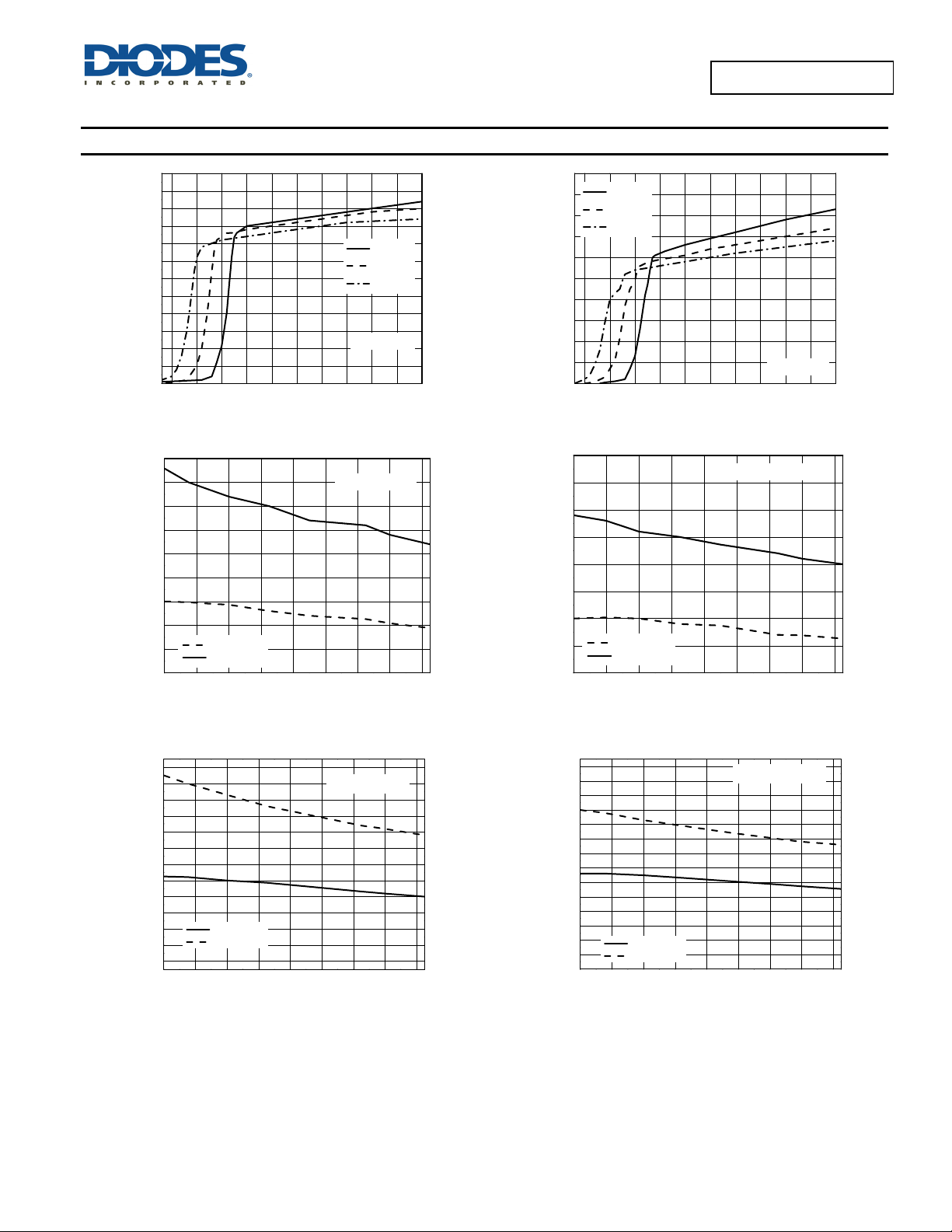
Typical Performance Characteristics (@T
60
55
50
45
40
35
30
25
20
Supply Current (μA)
15
10
5
0
123456
Supply Voltage (V)
Supply Current vs. Supply Voltage (LMV331)
80
75
70
ADVANCED INFORMATION
65
60
55
50
Supply Current (μA)
45
40
35
-40-20 0 20406080100120
Output High
Output Low
Temperature (OC)
VCC=5V, VEE=0V
Supply Current vs. Temperature (LMV331)
160
150
140
130
120
110
100
90
80
70
Supply Current (μA)
60
50
40
-40 - 20 0 20 40 60 80 100 120
Output High
Output Low
Tempareture (oC)
VCC=5V, VEE=0V
Supply Current vs. Temperature (LMV393)
LMV331/ LMV393
Document number: DS37022 Rev. 1 - 2
TA=-40oC
TA=25oC
TA=85oC
Output High
= +25°C, unless otherwise specified.)
A
100
TA=-40oC
90
TA=25oC
80
TA=85oC
70
60
50
40
30
Supply Current (μA)
20
10
0
123456
Supply Current vs. Supply Voltage (LMV331)
75
70
65
60
55
50
Supply Current (μA)
45
40
35
Output High
Output Low
-40 -20 0 20 40 60 80 100 120
Supply Current vs. Temperature (LMV331)
160
150
140
130
120
110
100
90
80
70
60
Supply Current (μA)
50
40
30
20
-40 - 20 0 20 40 60 80 100 120
Supply Current vs. Temperature (LMV393)
4 of 13
www.diodes.com
Supply Voltage (V)
Temperature (OC)
Output High
Output Low
LMV331/ LMV393
VCC=2.7V, VEE=0V
Tempareture (oC)
Output Low
VCC=2.7V, VEE=0V
© Diodes Incorporated
May 2014
 Loading...