

Page 1
Please click here to visit our online spice models database.
DPLS160
Features
• Epitaxial Planar Die Construction
• Complementary NPN Type Available (DNLS160)
• Surface Mount Package Suited for Automated Assembly
• Lead Free/RoHS Compliant (Note 1)
• "Green Device" (Note 2)
• Qualified to AEC-Q101 Standards for High Reliability
Mechanical Data
• Case: SOT-23
• Case Material: Molded Plastic, “Green” Molding
Compound. UL Flammability Classification Rating 94V-0
• Moisture Sensitivity: Level 1 per J-STD-020D
NEW PRODUCT
• Terminals: Finish ⎯ Matte Tin annealed over Copper
leadframe. Solderable per MIL-STD-202, Method 208
• Marking Information: See Page 4
• Ordering Information: See Page 4
• Weight: 0.008 grams (approximate)
Maximum Ratings @T
Collector-Base Voltage
Collector-Emitter Voltage
Emitter-Base Voltage
Collector Current - Continuous
Peak Pulse Collector Current
Base Current (DC)
= 25°C unless otherwise specified
A
Characteristic Symbol Value Unit
LOW V
V
CBO
V
CEO
V
EBO
I
C
I
CM
I
B
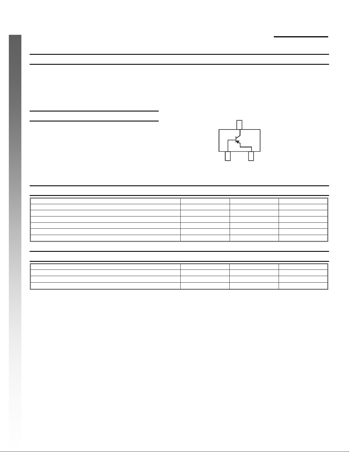
PNP SURFACE MOUNT TRANSISTOR
CE(SAT)
SOT-23
B
Schematic and Pin Configuration
C
E
-80 V
-60 V
-5 V
-1 A
-2 A
-300 mA
Thermal Characteristics
Characteristic Symbol Value Unit
Power Dissipation (Note 3) @ TA = 25°C PD
Thermal Resistance, Junction to Ambient (Note 3) @ TA = 25°C
Operating and Storage Temperature Range
Notes: 1. No purposefully added lead.
DS31389 Rev. 4 - 2 1 of 4
2. Diode’s Inc.’s “Green” policy can be found on our website at http://www.diodes.com/products/lead_free/index.php.
3. Device mounted on FR-4 PCB, 1 inch x 0.85 inch x 0.062 inch; pad layout as shown on page 4 or in Diodes Inc. suggested pad layout document
AP02001, which can be found on our website at http://www.diodes.com/datasheets/ap02001.pdf.
T
www.diodes.com
300 mW
R
JA
θ
, T
J
STG
417
-55 to +150
°C/W
°C
DPLS160
© Diodes Incorporated
Page 2
P, P
OWER
PATIO
N
C
O
CTO
R CUR
REN
T
Electrical Characteristics @T
= 25°C unless otherwise specified
A
Characteristic Symbol Min Typ Max Unit Test Condition
OFF CHARACTERISTICS (Note 4)
Collector-Base Breakdown Voltage
Collector-Emitter Breakdown Voltage
Emitter-Base Breakdown Voltage
Collector Cutoff Current
Collector Cutoff Current
Emitter Cutoff Current
V
(BR)CBO
V
(BR)CEO
V
(BR)EBO
I
I
I
ON CHARACTERISTICS (Note 4)
DC Current Gain
Collector-Emitter Saturation Voltage
NEW PRODUCT
Collector-Emitter Saturation Resistance
Base-Emitter Saturation Voltage
Base-Emitter Turn On Voltage
V
CE(SAT)
R
CE(SAT)
V
BE(SAT)
V
BE(ON)
SMALL SIGNAL CHARACTERISTICS
Output Capacitance
C
Current Gain-Bandwidth Product
Notes: 4. Measured under pulsed conditions. Pulse width = 300μs. Duty cycle ≤2%.
400
CBO
CES
EBO
h
FE
obo
f
T
-80
-60
-5
⎯ ⎯
⎯ ⎯
⎯ ⎯
200
150
100
⎯
⎯
⎯
⎯
⎯
⎯
⎯
150 220
⎯ ⎯
⎯ ⎯
⎯ ⎯
-100
-50
-100 nA
-100 nA
325
250
180
-90
-90
-160
⎯
⎯
⎯
-160
-175
-330
160 330 mΩ
-0.95 -1.1 V
-0.82 -0.9 V
10 15 pF
⎯
V
IC = -100μA, IE = 0
V
IC = -10mA, IB = 0
V
IE = -100μA, IC = 0
nA
V
= -60V, IE = 0
CB
μA
V
= -60V, IE = 0, TA = 150°C
CB
V
mV
VCE = -60V, V
V
= -5V, IC = 0
EB
= -5V, IC = -1mA
V
CE
= -5V, IC = -500mA
V
CE
V
= -5V, IC = -1A
CE
= -100mA, IB = -1mA
I
C
= -500mA, IB = -50mA
I
C
I
= -1A, IB = -100mA
C
BE
= 0
IC = -1A, IB = -100mA
IC = -1A, IB = -50mA
V
= -5V, IC = -1A
CE
VCB = -10V, f = 1.0MHz
MHz
VCE = -10V, IC = -50mA, f = 100MHz
1.5
350
I = -10mA
B
I = -8mA
B
I = -6mA
B
I = -4mA
B
I = -2mA
B
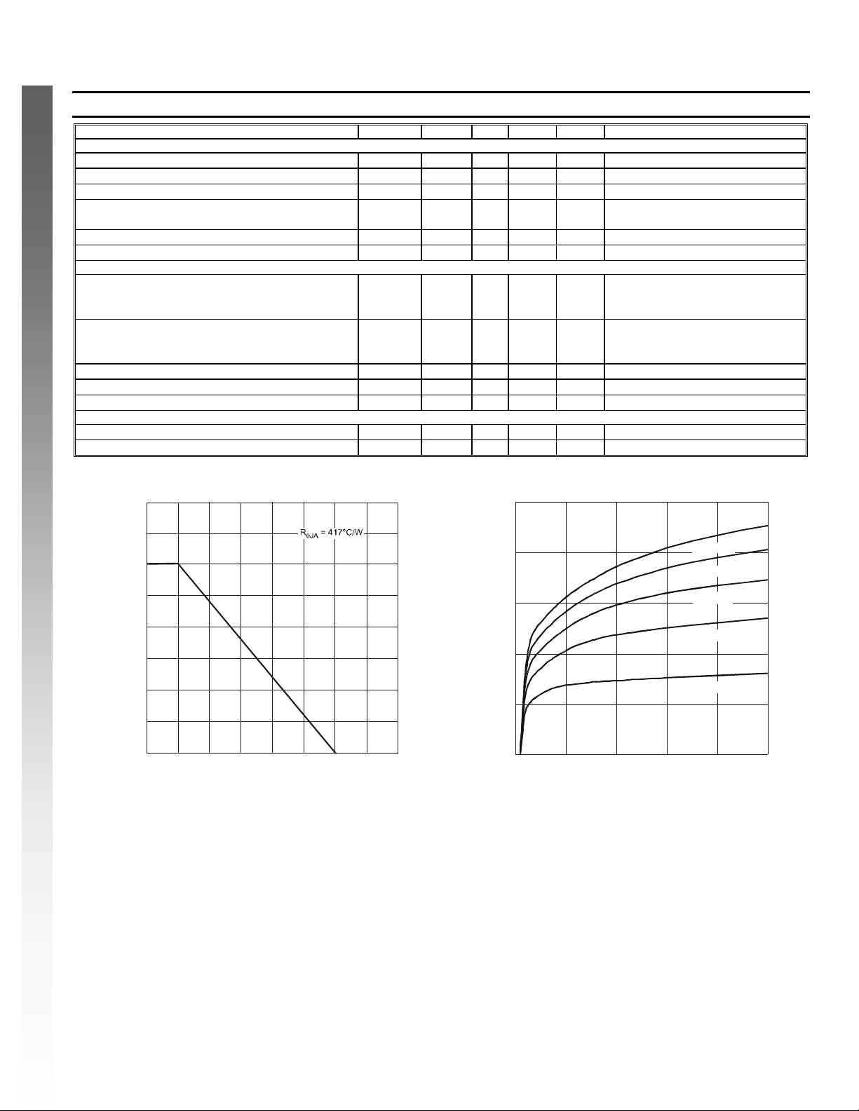
(mW)
DISSI
300
250
200
150
100
D
1.2
(A)
0.9
0.6
LLE
C
-I ,
0.3
50
0
0
25 50
T , AMBIENT TEMPERATURE (°C)
A
75
100 125
150
175
200
Fig. 1 Maximum Power Dissipation vs.
Ambient Temperature
0
01234
-V , COLLECTOR-EMITTER VOLTAGE (V)
CE
Fig. 2 Typical Collector Current
vs. Collector-Emitter Voltage
5
DS31389 Rev. 4 - 2 2 of 4
www.diodes.com
DPLS160
© Diodes Incorporated
Page 3

C CUR
REN
T
G
N
T
TER
TURATIO
OLTAG
600
AI
400
200
FE
h, D
0.4
0.3
0.2
0.1
SATURATION VOLTAGE (V)
CE(SAT)
-V , COLLECTOR EMITTER
0
NEW PRODUCT
0.001 0.01 0.1 1 10
-I , COLLECTOR CURRENT (A)
Fig. 3 Typical DC Current Gain vs. Collector Current
BE(ON)
-V , BASE EMITTER TURN-ON VOLTAGE (V)
0.001 0.01 0.1 1 10
-I , COLLECTOR CURRENT (A)
120
0
0.001 0.01 0.1 1 10
-I , COLLECTOR CURRENT (A)
C
C
1.2
E (V)
1.0
N V
0.8
T = -55°C
A
0.6
T = 25°C
A
SA
T = 85°C
A
0.4
T = 150°C
A
I/I = 20
CB
0.2
0
0.001 0.01 0.1 1 10
BE(SAT)
C
-V , BASE-EMI
-I , COLLECTOR CURRENT (A)
C
Fig. 6 Typical Base-Emitter Saturation Voltage
vs. Collector Current
250
100
C
ibo
f = 1MHz
200
80
150
60
100
40
CAPACITANCE (pF)
C
obo
20
0
0.01 0.1 1 10 100
V , REVERSE VOLTAGE (V)
R
Fig. 7 Typical Total Capacitance
50
0
T
f , CURRENT GAIN-BANDWIDTH PRODUCT (MHz)
0102030405060708090100
I , COLLECTOR CURRENT (mA)
C
Fig. 8 Typical Gain-Bandwidth Product
vs. Collector Current
DS31389 Rev. 4 - 2 3 of 4
www.diodes.com
V = -10V
CE
f = 100MHz
DPLS160
© Diodes Incorporated
Page 4

Ordering Information (Note 5)
Device Packaging Shipping
DPLS160-7 SOT-23 3000/Tape & Reel
Notes: 5. For packaging details, go to our website at http://www.diodes.com/datasheets/ap02007.pdf.
Marking Information
PK1 = Product Type Marking Code
PK1
Date Code Key
Year 2008 2009 2010 2011 2012 2013 2014 2015
NEW PRODUCT
Code V W X Y Z A B C
Month Jan Feb Mar Apr May Jun Jul Aug Sep Oct Nov Dec
Code 1 2 3 4 5 6 7 8 9 O N D
YM = Date Code Marking
Y = Year ex: U = 2007
YM
M = Month ex: 9 = September
Package Outline Dimensions
K
J
A
Dim Min Max
C
B
G
H
M
L
F
D
SOT-23
A 0.37 0.51
B 1.20 1.40
C 2.30 2.50
D 0.89 1.03
F 0.45 0.60
G 1.78 2.05
H 2.80 3.00
J 0.013 0.10
K 0.903 1.10
L 0.45 0.61
M 0.085 0.180
α
All Dimensions in mm
0° 8°
Suggested Pad Layout
Diodes Incorporated and its subsidiaries reserve the right to make modifications, enhancements, improvements, corrections or other changes
without further notice to any product herein. Diodes Incorporated does not assume any liability arising out of the application or use of any product
described herein; neither does it convey any license under its patent rights, nor the rights of others. The user of products in such applications shall
assume all risks of such use and will agree to hold Diodes Incorporated and all the companies whose products are represented on our website,
harmless against all damages.
Diodes Incorporated products are not authorized for use as critical components in life support devices or systems without the expressed written
approval of the President of Diodes Incorporated.
Y
Z
X E
C
IMPORTANT NOTICE
LIFE SUPPORT
Dimensions Value (in mm)
Z 2.9
X 0.8
Y 0.9
C 2.0
E 1.35
DS31389 Rev. 4 - 2 4 of 4
www.diodes.com
DPLS160
© Diodes Incorporated
 Loading...