Diodes DN0150BLP4 User Manual

Features
Epitaxial Die Construction
Ultra-Small Leadless Surface Mount Package
Ultra Low Profile (0.4mm max)
Complementary PNP Type: DP0150ALP4/DP0150BLP4
Totally Lead-Free & Fully RoHS compliant (Notes 1 & 2)
Halogen and Antimony Free. “Green” Device (Note 3)
Qualified to AEC-Q101 Standards for High Reliability
NEW PRODUCT
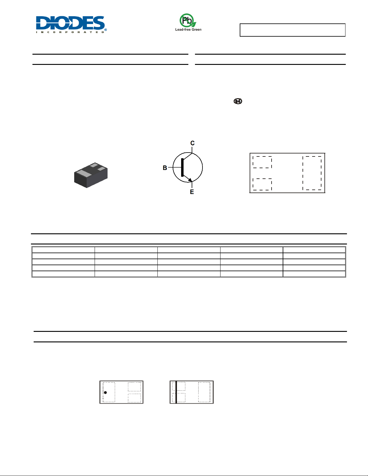
X2-DFN1006-3
Bottom View
50V NPN SMALL SIGNAL TRANSISTOR IN DFN1006
Mechanical Data
Case: X2-DFN1006-3
Case Material: Molded Plastic, "Green" Molding Compound.
Moisture Sensitivity: Level 1 per J-STD-020
Terminals: Finish NiPdAu, Solderable per MIL-STD-202,
Weight: 0.0008 grams (approximate)
Device Symbol
DN0150ALP4 / DN0150BLP4
UL Flammability Classification Rating 94V-0
Method 208
B
E
Top View
Pin Configuration
C
Ordering Information
Product Marking Reel size (inches) Tape width (mm) Quantity per reel
DN0150ALP4-7 T3 7 8 3,000
DN0150ALP4-7B T3 7 8 10,000
DN0150BLP4-7 T4 7 8 3,000
DN0150BLP4-7B T4 7 8 10,000
Notes: 1. No purposely added lead. Fully EU Directive 2002/95/EC (RoHS) & 2011/65/EU (RoHS 2) compliant.
2. See http://www.diodes.com/quality/lead_free.html for more information about Diodes Incorporated’s definitions of Halogen- and Antimony-free, "Green"
and Lead-free.
3. Halogen- and Antimony-free "Green” products are defined as those which contain <900ppm bromine, <900ppm chlorine (<1500ppm total Br + Cl) and
<1000ppm antimony compounds.
4. For packaging details, go to our website at http://www.diodes.com/products/packages.html.
(Note 4)
Marking Information
DN0150ALP4-7
DN0150BLP4-7
XX XX
Top View
Dot Denotes
Collector Side
DN0150ALP4-7B
DN0150BLP4-7B
XX = Product Type Marking Code
(See Ordering Information)
Top View
Bar Denotes Base
and Emitter Side
DN0150ALP4 / DN0150BLP4
Document number: DS31492 Rev. 5 - 2
1 of 5
www.diodes.com
December 2013
© Diodes Incorporated

)
Absolute Maximum Ratings (@T
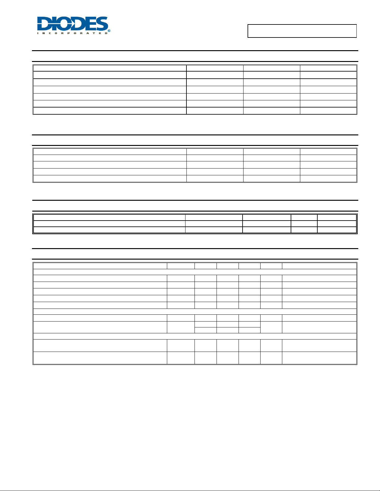
Characteristic Symbol Value Unit
Collector-Base Voltage
Collector-Emitter Voltage
Emitter-Base Voltage
Collector Current – Continuous
Peak Pulse Collector Current
Base Current
Thermal Characteristics (@T
Characteristic Symbol Value Unit
Power Dissipation (Note 5)
NEW PRODUCT
Thermal Resistance, Junction to Ambient (Note 5)
Thermal Resistance, Junction to Leads (Note 6)
Operating and Storage Temperature Range
ESD Ratings (Note 7)
= +25°C, unless otherwise specified.)
A
V
CBO
V
CEO
V
EBO
I
C
I
CM
I
B
= +25°C, unless otherwise specified.)
A
P
D
R
JA
R
θJL
T
, T
J
STG
DN0150ALP4 / DN0150BLP4
60 V
50 V
5 V
100 mA
200 mA
30 mA
450 mW
278 °C/W
110 °C/W
-55 to +150 °C
Electrostatic Discharge - Human Body Model ESD HBM 4,000 V 3A
Characteristic Symbol Value Unit JEDEC Class
Electrostatic Discharge - Machine Model ESD MM 400 V C
Electrical Characteristics (@T
= +25°C, unless otherwise specified.)
A
Characteristic Symbol Min Typ Max Unit Test Condition
OFF CHARACTERISTICS
Collector-Base Breakdown Voltage
Collector-Emitter Breakdown Voltage (Note 8)
Emitter-Base Breakdown Voltage
Collector Cut-Off Current
Emitter Cut-Off Current
BV
BV
BV
I
CBO
I
EBO
CBO
CEO
EBO
60 — — V
50 — — V
5 — — V
— — 0.1 μA
— — 0.1 μA
IC = 10μA, IE = 0
IC = 1mA, IB = 0
IE = 10μA, IC = 0
VCB = 60V, IE = 0
VEB = 5V, IC = 0
ON CHARACTERISTICS (Note 8)
Collector-Emitter Saturation Voltage
DC Current Gain DN0150ALP4
DN0150BLP4
V
CE(SAT
h
FE
— 0.10 0.25 V
120 — 240
200 — 400
IC = 100mA, IB = 10mA
—
VCE = 6V, IC = 2mA
SMALL SIGNAL CHARACTERISTICS
= 10V, IE = -1mA
V
Transition Frequency
Output Capacitance
Notes: 5. For a device mounted on minimum recommended pad layout 1oz copper that is on a single-sided FR-4 PCB; device is measured under still air
conditions whilst operating in a steady-state. The entire exposed collector pad is attached to the heat sink.
6. Thermal resistance from junction to solder-point (at the end of the collector lead).
7. Refer to JEDEC specification JESD22-A114 and JESD22-A115.
f
T
C
ob
60 — — MHz
— 1.3 — pF
CE
f = 30MHz
= 10V, IE = 0,
V
CB
f = 1MHz
8. Measured under pulsed conditions. Pulse width 300µs. Duty cycle 2%
DN0150ALP4 / DN0150BLP4
Document number: DS31492 Rev. 5 - 2
2 of 5
www.diodes.com
December 2013
© Diodes Incorporated
 Loading...