Diodes DMS3017SSD User Manual

ASYMMETRIC DUAL N-CHANNEL ENHANCEMENT MODE MOSFET
Features
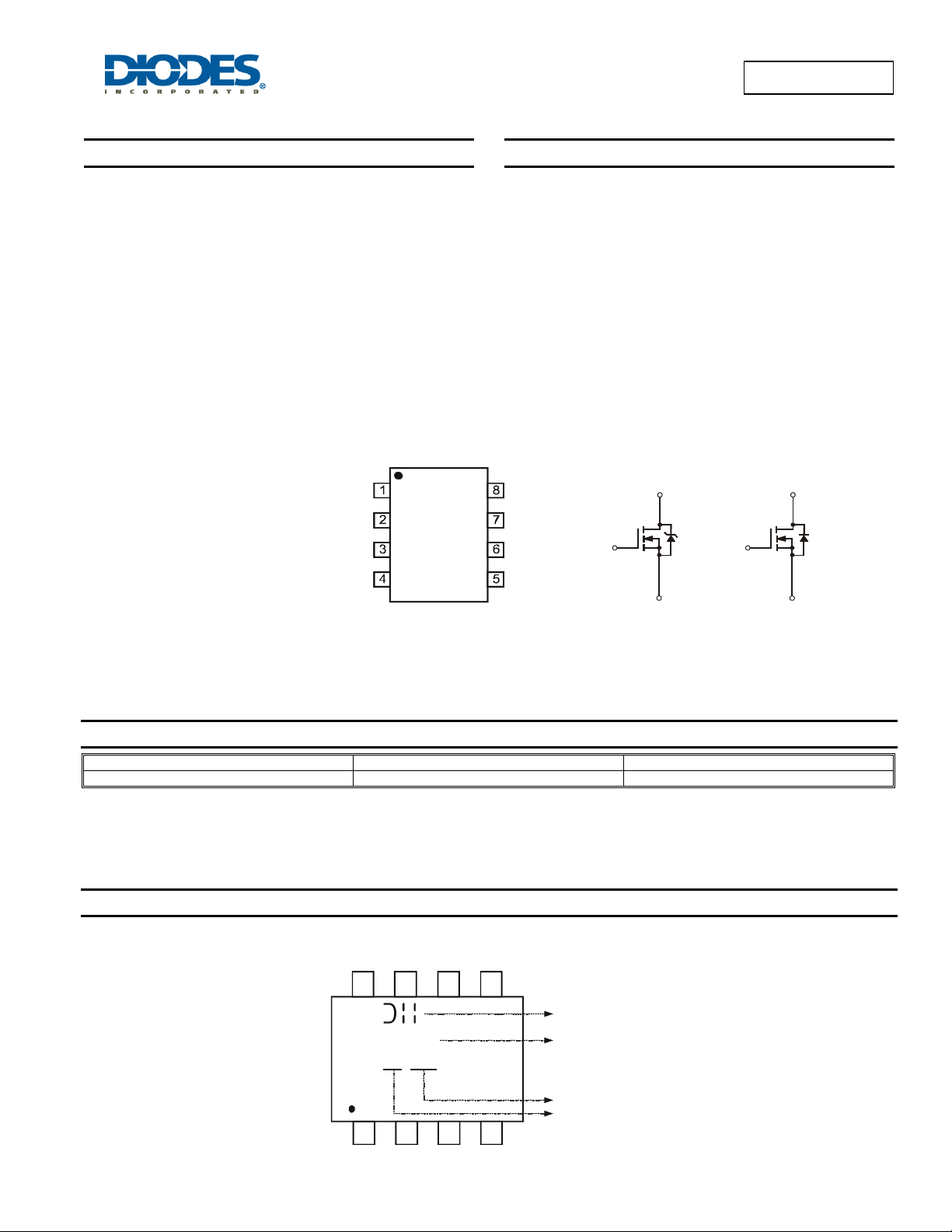
• DIOFET utilize a unique patented process to monolithically
integrate a MOSFET and a Schottky in a single die to deliver:
• Low R
• Low V
construction
• Low Q
diode switching losses
• Low gate capacitance (Q
through or cross conduction currents at high frequencies
• Avalanche rugged – I
• Lead Free By Design/RoHS Compliant (Note 1)
• "Green" Device (Note 2)
• Qualified to AEC-Q101 Standards for High Reliability
– minimizes conduction loss
DS(on)
– reducing the losses due to body diode
SD
– lower Qrr of the integrated Schottky reduces body
rr
) ratio – reduces risk of shoot-
g/Qgs
and EAR rated
AR
D2
D2
G1
S1
Top View
Top View
Internal Schematic
DMS3017SSD
Mechanical Data
• Case: SO-8
• Case Material: Molded Plastic, “Green” Molding Compound.
UL Flammability Classification Rating 94V-0
• Moisture Sensitivity: Level 1 per J-STD-020
• Terminal Connections: See Diagram Below
• Weight: 0.072 grams (approximate)
Q1 Q2
G2
S2/D1
S2/D1
S2/D1
D
1
G
1
S
1
Integrat ed Schottky Diode
G
2
N-Channel MOSFETN-Channel MOSFET +
D
2
S
2
Ordering Information (Note 3)
Part Number Case Packaging
DMS3017SSD-13 SO-8 2500 / Tape & Reel
Notes: 1. No purposefully added lead.
2. Diodes Inc.'s "Green" policy can be found on our website at http://www.diodes.com/products/lead_free/index.php.
3. For packaging details, go to our website at http://www.diodes.com/datasheets/ap02007.pdf.
Marking Information
DMS3017SSD
Document number: DS35052 Rev. 2 - 2
Top View
8 5
S3017SD
WW
YY
1 4
www.diodes.com
1 of 10
Logo
Part no.
Week: 01 ~ 53
Y ear: “09” = 2009
October 2010
© Diodes Incorporated

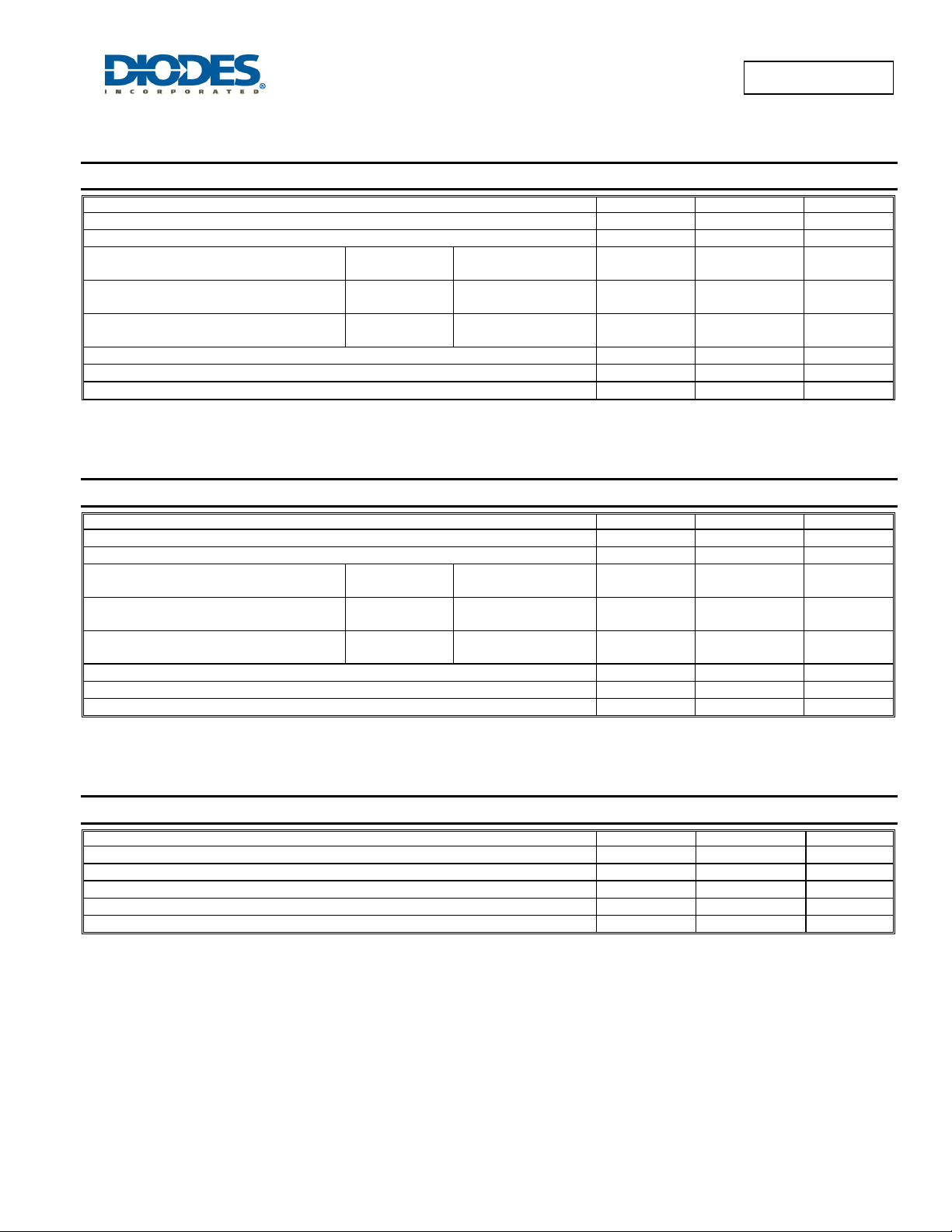
Maximum Ratings – Q1 @TA = 25°C unless otherwise specified
Characteristic Symbol Value Unit
Drain-Source Voltage
Gate-Source Voltage
T
Continuous Drain Current (Note 4) VGS = 10V
Continuous Drain Current (Note 5) VGS = 10V
Continuous Drain Current (Note 5) VGS = 4.5V
Pulsed Drain Current (Note 6)
Avalanche Current (Notes 6 & 7)
Repetitive Avalanche Energy (Notes 6 & 7) L = 0.1mH
Steady
State
Steady
State
Steady
State
= 25°C
A
T
= 70°C
A
= 25°C
T
A
= 70°C
T
A
T
= 25°C
A
T
= 70°C
A
DMS3017SSD
V
DSS
V
GSS
I
D
I
D
I
D
I
DM
I
AR
E
AR
30 V
±20 V
8.0
6.5
10
7.8
8.7
7.0
A
A
A
60 A
16 A
12.8 mJ
Maximum Ratings – Q2 @TA = 25°C unless otherwise specified
Characteristic Symbol Value Unit
Drain-Source Voltage
Gate-Source Voltage
Continuous Drain Current (Note 4) VGS = 10V
Continuous Drain Current (Note 5) VGS = 10V
Continuous Drain Current (Note 5) VGS = 4.5V
Pulsed Drain Current (Note 6)
Avalanche Current (Notes 6 & 7)
Repetitive Avalanche Energy (Notes 6 & 7) L = 0.1mH
Steady
State
Steady
State
Steady
State
T
= 25°C
A
= 70°C
T
A
T
= 25°C
A
T
= 70°C
A
= 25°C
T
A
= 70°C
T
A
V
DSS
V
GSS
I
D
I
D
I
D
I
DM
I
AR
E
AR
30 V
±20 V
6.0
4.7
7.2
6.0
6.0
5.0
A
A
A
60 A
16 A
12.8 mJ
Thermal Characteristics
Characteristic Symbol Value Unit
Power Dissipation (Note 4)
Thermal Resistance, Junction to Ambient @T
= 25°C (Note 4) R
A
Power Dissipation (Note 5)
Thermal Resistance, Junction to Ambient @T
= 25°C (Note 5) R
A
Operating and Storage Temperature Range
Notes: 4. Device mounted on FR-4 substrate PC board, with minimum recommended pad layout. The value in any given application depends on the user’s specific
board design. Device contains two active die running at equal power.
5. Device mounted on 1 inch x 1 inch FR4 PCB with high coverage of single sided 1oz copper, in still air conditions. Device contains two active die running
at equal power.
6. Repetitive rating, pulse width limited by junction temperature.
7. I
and EAR rating are based on low frequency and duty cycles to keep TJ = 25°C
AR
P
D
θJA
P
D
θJA
T
, T
J
STG
1.19 W
107 °C/W
1.79 W
70 °C/W
-55 to +150 °C
DMS3017SSD
Document number: DS35052 Rev. 2 - 2
2 of 10
www.diodes.com
October 2010
© Diodes Incorporated

)
g
g
g
)
r
)
R
C
URRENT
R
C
URRENT
DMS3017SSD
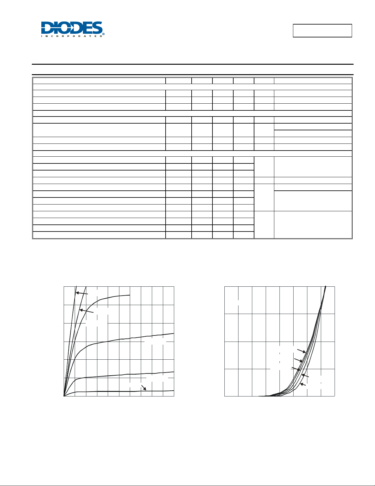
Electrical Characteristics – Q1 @ T
= 25°C unless otherwise stated
A
Characteristic Symbol Min Typ Max Unit Test Condition
OFF CHARACTERISTICS (Note 8)
Drain-Source Breakdown Voltage
Zero Gate Voltage Drain Current
Gate-Source Leakage
BV
I
I
ON CHARACTERISTICS (Note 8)
Gate Threshold Voltage
Static Drain-Source On-Resistance
Forward Transfer Admittance
Diode Forward Voltage
V
GS(th
R
DS (ON)
|Y
V
DYNAMIC CHARACTERISTICS (Note 9)
Input Capacitance
Output Capacitance
Reverse Transfer Capacitance
C
C
C
Gate Resistance
Total Gate Charge (VGS = 4.5V) Qg
Total Gate Charge (VGS = 10V) Qg
Gate-Source Charge
Gate-Drain Charge
Turn-On Delay Time
Q
Q
t
D(on
Turn-On Rise Time
Turn-Off Delay Time
t
D(off
Turn-Off Fall Time
Notes: 8. Short duration pulse test used to minimize self-heating effect.
9. Guaranteed by design. Not subject to production testing.
30
V = 10V
GS
25
V = 4.5V
GS
(A)
20
V = 4.0V
GS
DSS
DSS
GSS
SD
iss
oss
rss
R
t
t
30 - - V
- - 100 μA
- - ±100 nA
1.0 - 2.5 V
|
fs
9.5
- 18 - S
- 0.45 0.60 V
- 1276 -
- 160 -
- 136 -
- 1.48 2.7
8.5
-
12
15
- 14.3 -
- 30.6 -
s
d
f
- 3.4 -
- 4.3 -
- 15.8 -
- 27.8 -
- 29.7 -
- 13.6 -
VGS = 0V, ID = 250μA
VDS = 30V, VGS = 0V
VGS = ±20V, VDS = 0V
VDS = VGS, ID = 250μA
= 10V, ID = 9.5A
V
mΩ
GS
VGS = 4.5V, ID = 8.8A
VDS = 5V, ID = 9.5A
VGS = 0V, IS = 1A
= 15V, VGS = 0V,
V
DS
pF
f = 1.0MHz
Ω
VDS = 0V, VGS = 0V, f = 1MHz
VDS = 15V, VGS = 4.5V, ID = 8.8A
nC
= 15V, VGS = 10V, ID = 8.8A
V
DS
= 4.5V, VDS = 15V,
V
GS
ns
= 1.8Ω, ID = 8.8A
R
G
20
V = 5V
DS
15
(A)
15
AIN
10
D
I, D
5
V = 2.5V
GS
0
0 0.5 1 1.5 2 2.5 3 3.5 4 4.5 5
V , DRAIN-SOURCE VOLT AGE (V)
DS
Fig. 1 Typical Output Ch ar acteristic
V = 3.5V
GS
V = 3.0V
GS
10
V = 150°C
AIN
D
I, D
5
0
0 0.5 1 1.5 2 2.5 3 3.5 4
V , GATE-SOURCE VOLT AGE (V)
GS
Fig. 2 Typical Transfer Characteristic
GS
V = 125°C
GS
V = 85°C
GS
V = -55°C
V = 25°C
GS
GS
DMS3017SSD
Document number: DS35052 Rev. 2 - 2
3 of 10
www.diodes.com
October 2010
© Diodes Incorporated
 Loading...