Diodes DMS3016SFG User Manual

N-CHANNEL ENHANCEMENT MODE MOSFET WITH SCHOTTKY DIODE
Product Summary
I
V
R
(BR)DSS
30V
13mΩ @ V
16mΩ @ VGS = 4.5V
DS(on) max
GS
= 10V
D
TA = 25°C
10.2A
9.3A
Description
This new generation MOSFET has been designed to minimize the onstate resistance (R
performance, making it ideal for high efficiency power management
applications.
) and yet maintain superior switching
DS(on)
Applications
• DC-DC Converters
• Power management functions
• Analog Switch
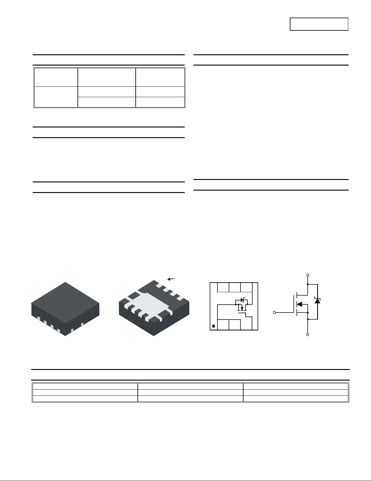
Top View Bottom View
POWERDI3333-8
D
S
D
D
D
S
Pin 1
S
Green
DMS3016SFG
Features and Benefits
• DIOFET utilizes a unique patented process to monolithically
integrate a MOSFET and a Schottky in a single die to deliver:
• Low R
• Low V
• Low Q
switching losses
• Low gate capacitance (Q
through or cross conduction currents at high frequencies
• Avalanche rugged – I
• Small form factor thermally efficient package enables higher
density end products
• Occupies just 33% of the board area occupied by SO-8 enabling
smaller end product
• Lead-Free Finish; RoHS Compliant (Notes 1 & 2)
• Halogen and Antimony Free. “Green” Device (Note 3)
• Qualified to AEC-Q101 Standards for High Reliability
– minimize conduction losses
DS(ON)
– reducing the losses due to body diode conduction
SD
– lower Qrr of the integrated Schottky reduces body diode
rr
) ratio – reduces risk of shoot-
g/Qgs
and EAR rated
AR
Mechanical Data
• Case: POWERDI3333-8
• Case Material: Molded Plastic, “Green” Molding Compound.
• UL Flammability Classification Rating 94V-0
• Moisture Sensitivity: Level 1 per J-STD-020
• Terminal Connections: See Diagram
• Terminals: Finish ⎯ Matte Tin annealed over Copper leadframe.
Solderable per MIL-STD-202, Method 208
• Weight: 0.072 grams (approximate)
8765
G
Gate
234
1
Top View
Pin Configuration
Drain
Source
Internal Schematic
POWERDI
®
Ordering Information (Note 4)
Part Number Case Packaging
DMS3016SFG-7 POWERDI3333-8 2,000/Tape & Reel
DMS3016SFG-13 POWERDI3333-8 3,000/Tape & Reel
Notes: 1. EU Directive 2002/95/EC (RoHS) & 2011/65/EU (RoHS 2) compliant. All applicable RoHS exemptions applied.
2. See http://www.diodes.com for more information about Diodes Incorporated’s definitions of Halogen- and Antimony-free, "Green" and Lead-free.
POWERDI is a registered trademark of Diodes Incorporated.
DMS3016SFG
Document number: DS35434 Rev. 7 - 2
3. Halogen- and Antimony-free "Green” products are defined as those which contain <900ppm bromine, <900ppm chlorine (<1500ppm total Br + Cl) and
<1000ppm antimony compounds.
4. For packaging details, go to our website at http://www.diodes.com.
1 of 7
www.diodes.com
October 2012
© Diodes Incorporated

θ
P, P
T
R
N
N
T
P
O
R
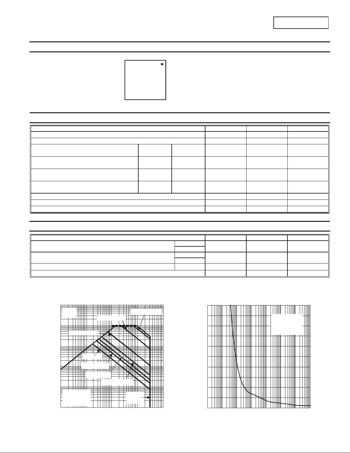
Marking Information
Maximum Ratings (@T
Drain-Source Voltage
Gate-Source Voltage
Continuous Drain Current (Note 5) VGS = 10V
Continuous Drain Current (Note 5) VGS = 4.5V
Continuous Drain Current (Note 6) VGS = 10V
Continuous Drain Current (Note 6) VGS = 4.5V
Pulsed Drain Current (10us pulse, duty cycle=1%)
Avalanche Current (Note 7)
Repetitive Avalanche Energy (Note 7) L = 0.3mH
= +25°C, unless otherwise specified.)
A
Characteristic Symbol Value Units
S30
YYWW
Steady
State
Steady
State
Steady
State
Steady
State
S30 = Product Type Marking Code
YYWW = Date Code Marking
YY = Last digit of year (ex: 09 = 2009)
WW = Week code (01 ~ 53)
V
DSS
V
GSS
T
= +25°C
A
= +70°C
T
A
T
= +25°C
A
T
= +70°C
A
T
= +25°C
A
= +70°C
T
A
T
= +25°C
A
T
= +70°C
A
I
D
I
D
I
D
I
D
I
DM
I
AR
E
AR
DMS3016SFG
30 V
±12 V
7.0
5.5
6.4
5.1
10.2
8.1
9.3
7.4
80 A
13 A
24 mJ
A
A
A
A
Thermal Characteristics (@T
= +25°C, unless otherwise specified.)
A
Characteristic Symbol Value Units
Total Power Dissipation
Thermal Resistance, Junction to Ambient
(Note 5)
(Note 6)
(Note 5)
(Note 6)
Thermal Resistance, Junction to Case (Note 6)
Operating and Storage Temperature Range
Notes: 5. Device mounted on FR-4 PC board, with minimum recommended pad layout, single sided.
6. Device mounted on FR-4 substrate PC board, 2oz copper, with thermal vias to bottom layer 1inch square copper plate
7 .I
and EAR rating are based on low frequency and duty cycles to keep TJ = +25°C
AR
1,000
R
DS(ON)
Limited
I(A) @P =1ms
DW
I(A) @P =100µs
DW
100
I(A) @P =10ms
DW
10
I (A) @ DC
D
I(A) @P =10s
1
D
I , DRAIN CURRENT (A)
0.1
T = 150 C
J(MAX)
T= 25C
A
Single Pulse
0.01
0.01 0.1 1 10 100
DW
I(A) @P =1s
DW
I(A) @P =100ms
DW
°
°
V , DRAIN-SOURCE VOLTAGE (V)
DS
I(A) @
D
P=10µs
W
(W)
IWE
SIE
A
EAK
100
90
80
70
60
50
40
30
20
(PK)
10
0
Fig. 1 SOA, Safe Oper ation Area
P
R
R
T
J, TSTG
D
JA
θ
JC
0.98
2.08
127
60
°C/W
3.42 °C/W
-55 to +150 °C
Single Pulse
°
R = 54C/W
θ
JA
R = r * R
θθ
JA(t) (t) JA
T - T = P * R
JA JA(t)
θ
0.001 0.01 0.1 1 10 100 1,0000.0001
t1, PULSE DURATION TIME (sec)
Fig. 2 Single Pulse Maximum Power Dissipation
W
POWERDI is a registered trademark of Diodes Incorporated.
DMS3016SFG
Document number: DS35434 Rev. 7 - 2
2 of 7
www.diodes.com
October 2012
© Diodes Incorporated

)
g
g
)
r
)
1
D = 0.7
D = 0.5
D = 0.3
0.1
D = 0.1
D = 0.05
D = 0.02
0.01
D = 0.01
D = 0.005
r(t), TRANSIENT THERMAL RESISTANCE
Single Puls e
0.001
0.00001 0.0001 0.001 0.01 0.1 1 10 100 1,000
t1, PULSE DURATION TIMES (sec)
D = 0.9
R(t)=r(t) * R
θ
JA
R = 54°C/W
JA
Duty Cycle, D = t1/ t2
θθJA
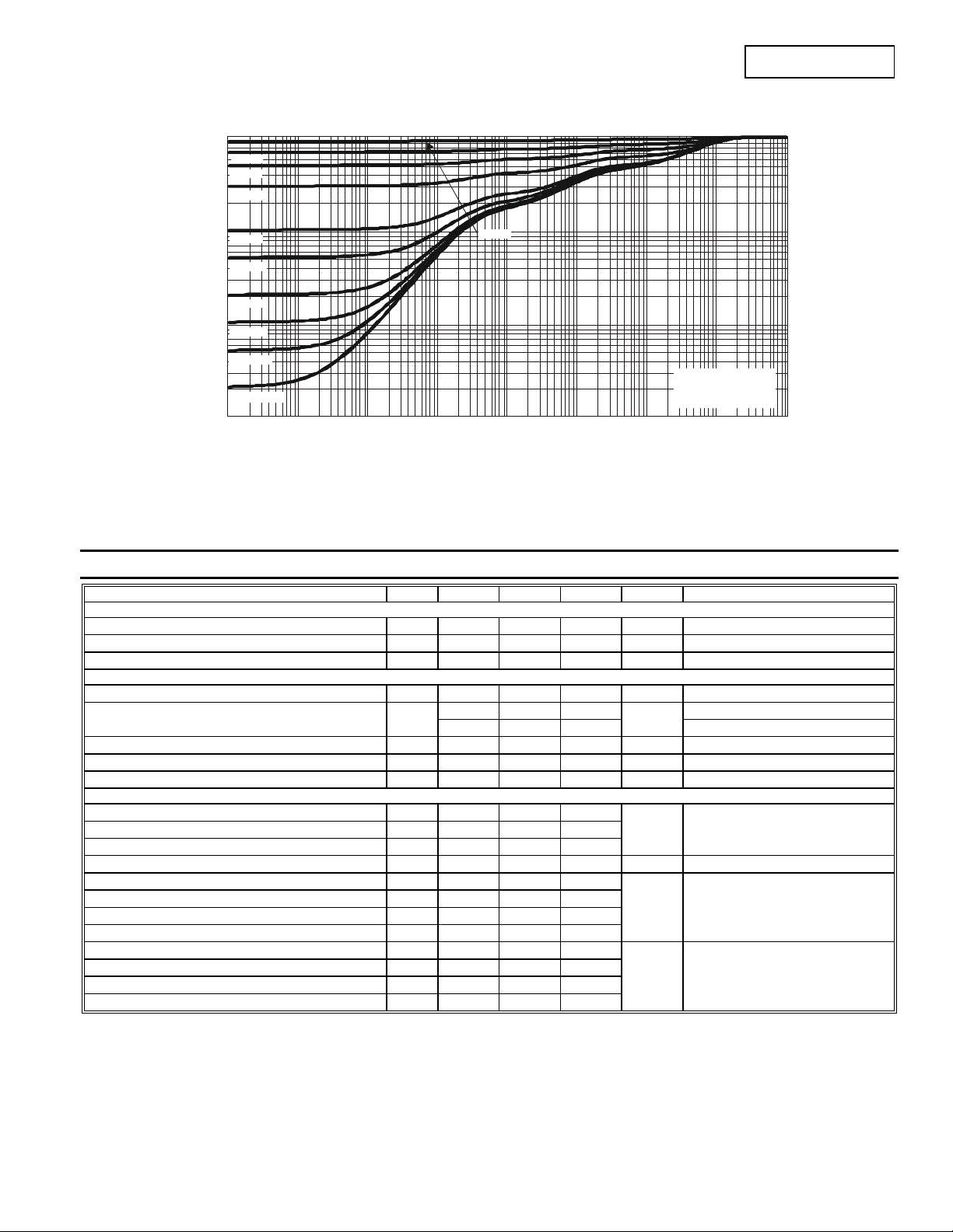
Fig. 3 Transient Thermal Resistance
DMS3016SFG
Electrical Characteristics (@T
= +25°C, unless otherwise specified.)
A
Characteristic Symbol Min Typ Max Unit Test Condition
OFF CHARACTERISTICS (Note 8)
Drain-Source Breakdown Voltage
Zero Gate Voltage Drain Current
Gate-Source Leakage
BV
I
DSS
I
GSS
DSS
30
⎯ ⎯
⎯ ⎯
⎯ ⎯
100
±100
V
VGS = 0V, ID = 1mA
µA
V
nA
DS
V
GS
= 30V, VGS = 0V
= ±12V, VDS = 0V
ON CHARACTERISTICS (Note 8)
Gate Threshold Voltage
Static Drain-Source On-Resistance
Forward Transfer Admittance
Diode Forward Voltage
Maximum Body-Diode + Schottky Continuous Current
V
R
DS(ON)
|Y
V
GS(th
fs
SD
I
S
1.0
⎯
⎯
| ⎯
⎯
⎯
10 13
12 16
25
0.37 0.6 V
⎯ ⎯
2.2 V
mΩ
⎯
VDS = VGS, ID = 250μA
= 10V, ID = 11.2A
V
GS
VGS = 4.5V, ID = 10.A
S
V
= 5V, ID = 11.2A
DS
VGS = 0V, IS = 1A
5 A
DYNAMIC CHARACTERISTICS (Note 9)
Input Capacitance
Output Capacitance
Reverse Transfer Capacitance
Gate Resistance
C
iss
C
oss
C
rss
R
G
Total Gate Charge (VGS = 4.5V) Qg
Total Gate Charge (VGS = 10V) Qg
Gate-Source Charge
Gate-Drain Charge
Turn-On Delay Time
Turn-On Rise Time
Turn-Off Delay Time
Turn-Off Fall Time
Notes: 8 .Short duration pulse test used to minimize self-heating effect.
9. Guaranteed by design. Not subject to production testing.
t
t
Q
Q
D(on
D(off
s
d
t
t
f
⎯
⎯
⎯
⎯
⎯
⎯
⎯
⎯
⎯
⎯
⎯
⎯
1886
372
128
2.0
19.5
44.6
4.8
4.6
5.8
23.7
35.4
7.7
⎯
⎯
pF
⎯
⎯ Ω
⎯
⎯
⎯
nC
⎯
⎯
⎯
⎯
ns
⎯
V
= 15V, VGS = 0V
DS
f = 1.0MHz
VDS = 0V, VGS = 0V, f = 1.0MHz
V
= 15V, VGS = 10V
DS
I
= 11.2A
D
V
= 10V, VDD = 15V, RG = 3Ω,
GS
R
= 1.2Ω
L
POWERDI is a registered trademark of Diodes Incorporated.
DMS3016SFG
Document number: DS35434 Rev. 7 - 2
3 of 7
www.diodes.com
October 2012
© Diodes Incorporated
 Loading...