Diodes DMS3014SFG User Manual

DMS3014SFG
30V N-CHANNEL ENHANCEMENT MODE MOSFET
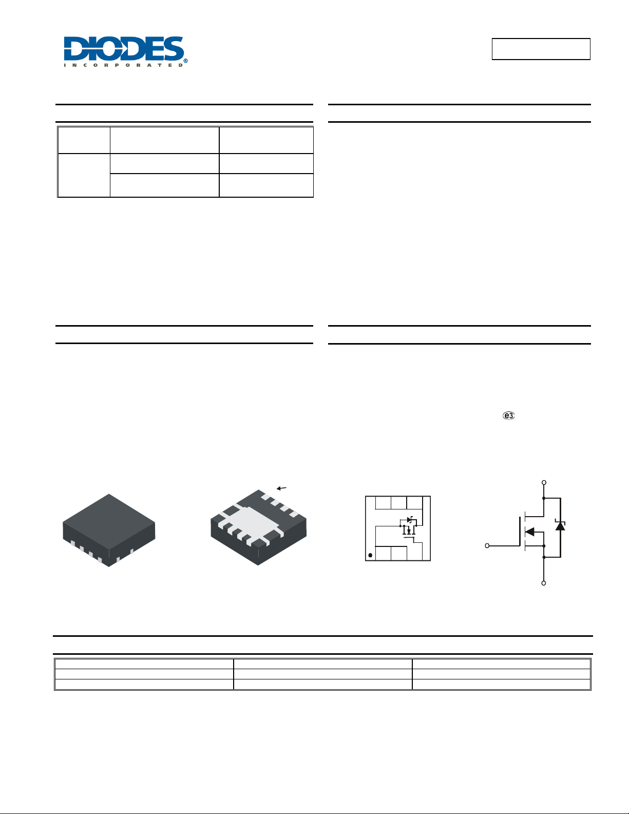
POWERDI
®
Pin 1
S
Features and Benefits
• DIOFET utilizes a unique patented process to monolithically
integrate a MOSFET and a Schottky in a single die to deliver:
• Low R
• Low V
• Low Q
– minimize conduction losses
DS(ON)
– reducing the losses due to body diode conduction
SD
– lower Qrr of the integrated Schottky reduces body
rr
diode switching losses
• Low gate capacitance (Q
) ratio – reduces risk of shoot-
g/Qgs
through or cross conduction currents at high frequencies
• Small form factor thermally efficient package enables higher
density end products
• Occupies just 33% of the board area occupied by SO-8 enabling
smaller end product
• 100% UIS (Avalanche) rated
• 100% Rg tested
• Totally Lead-Free & Fully RoHS Compliant (Notes 1 & 2)
• Halogen and Antimony Free. “Green” Device (Note 3)
• Qualified to AEC-Q101 Standards for High Reliability
Mechanical Data
• Case: POWERDI3333-8
• Case Material: Molded Plastic, "Green" Molding Compound.
UL Flammability Classification Rating 94V-0
• Moisture Sensitivity: Level 1 per J-STD-020
• Terminal Connections Indicator: See diagram
• Terminals: Finish ⎯ Matte Tin annealed over Copper leadframe.
Solderable per MIL-STD-202, Method 208
• Weight: 0.072 grams (approximate)
Drain
8765
G
Gate
234
1
Top View
Pin Configuration
Internal Schematic
Source
Product Summary
I
max
D
V
(BR)DSS
R
13m @ V
DS(ON)
max
= 10V
GS
TA = 25°C
9.5A
30V
14m @ VGS = 4.5V
9.0A
ADVANCE INFORMATION
Description and Applications
This MOSFET has been designed to minimize the on-state resistance
(R
) and yet maintain superior switching performance, making it
DS(on)
ideal for high efficiency power management applications.
• Backlighting
• Power Management Functions
• DC-DC Converters
Top View
D
D
D
D
S
S
Bottom View
Ordering Information (Note 4)
Part Number Case Packaging
DMS3014SFG-7 POWERDI3333-8 2000/Tape & Reel
DMS3014SFG-13 POWERDI3333-8 3000/Tape & Reel
Notes: 1. No purposely added lead. Fully EU Directive 2002/95/EC (RoHS) & 2011/65/EU (RoHS 2) compliant.
2. See http://www.diodes.com for more information about Diodes Incorporated’s definitions of Halogen- and Antimony-free, "Green" and Lead-free.
4. For packaging details, go to our website at http://www.diodes.com.
POWERDI is a registered trademark of Diodes Incorporated
DMS3014SFG
Document number: DS35594 Rev. 6 - 2
3. Halogen- and Antimony-free "Green” products are defined as those which contain <900ppm bromine, <900ppm chlorine (<1500ppm total Br + Cl) and
<1000ppm antimony compounds.
1 of 8
www.diodes.com
© Diodes Incorporated
May 2012

θ
DMS3014SFG
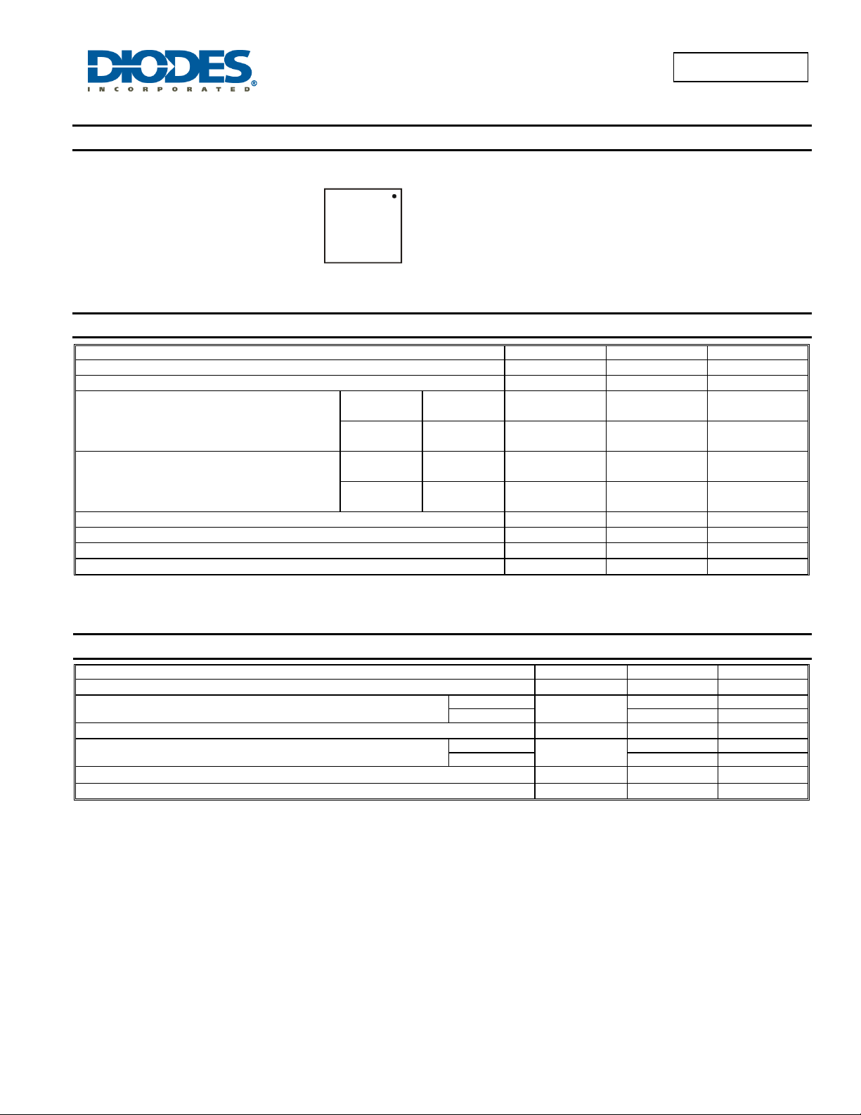
Marking Information
Maximum Ratings @T
Drain-Source Voltage
Gate-Source Voltage
ADVANCE INFORMATION
Continuous Drain Current (Note 6) VGS = 10V
Continuous Drain Current (Note 6) VGS = 4.5V
Pulsed Drain Current (10s pulse, duty cycle = 1%)
Maximum Continuous Body Diode Forward Current (Note 6)
Avalanche Current (Note 7) L = 0.1mH
Repetitive Avalanche Energy (Note 7) L = 0.1mH
S29 = Product Type Marking Code
YYWW
S29
= 25°C unless otherwise specified
A
YYWW = Date Code Marking
YY = Last digit of year (ex: 11 = 2011)
WW = Week code (01 ~ 53)
Characteristic Symbol Value Units
30 V
±12 V
9.5
7.6
13.0
9.7
9.0
7.4
12.2
9.3
A
A
A
A
80 A
3.0 A
30 A
45 mJ
Steady
State
t<10s
Steady
State
t<10s
T
= 25°C
A
= 70°C
T
A
T
= 25°C
A
T
= 70°C
A
T
= 25°C
A
= 70°C
T
A
T
= 25°C
A
T
= 70°C
A
V
DSS
V
GSS
I
D
I
D
I
D
I
D
I
DM
I
S
I
AR
E
AR
Thermal Characteristics @T
= 25°C unless otherwise specified
A
Characteristic Symbol Value Units
Total Power Dissipation (Note 5)
Thermal Resistance, Junction to Ambient (Note 5)
Steady state
t<10s 72 °C/W
Total Power Dissipation (Note 6)
Thermal Resistance, Junction to Ambient (Note 6)
Steady state
t<10s 35 °C/W
Thermal Resistance, Junction to Case (Note 6)
Operating and Storage Temperature Range
Notes: 5. Device mounted on FR-4 substrate PC board, 2oz copper, with minimum recommended pad layout.
6. Device mounted on FR-4 substrate PC board, 2oz copper, with 1inch square copper plate.
7. I
and EAR rating are based on low frequency and duty cycles to keep TJ = 25°C
AR
P
R
P
R
R
T
J, TSTG
D
JA
θ
D
JA
θ
JC
1 W
131 °C/W
2.1 W
63 °C/W
7.1 °C/W
-55 to +150 °C
POWERDI is a registered trademark of Diodes Incorporated
DMS3014SFG
Document number: DS35594 Rev. 6 - 2
2 of 8
www.diodes.com
May 2012
© Diodes Incorporated

R
C
URRENT
P, P
T
R
T P
O
R
θ
T
R
T T
HER
R
TANC
DMS3014SFG
100
R
DS(on)
Limited
P = 10sWµ
10
(A)
DC
P = 10s
1
AIN
D
0.1
-I , D
0.01
0.1 1 10
ADVANCE INFORMATION
W
P = 1s
W
P = 100ms
W
P = 10ms
W
P = 1ms
W
P = 100µs
W
T = 150°C
J(max)
T = 25°C
A
Single Pulse
-V , DRAIN-SOURCE VOLTAGE (V)
DS
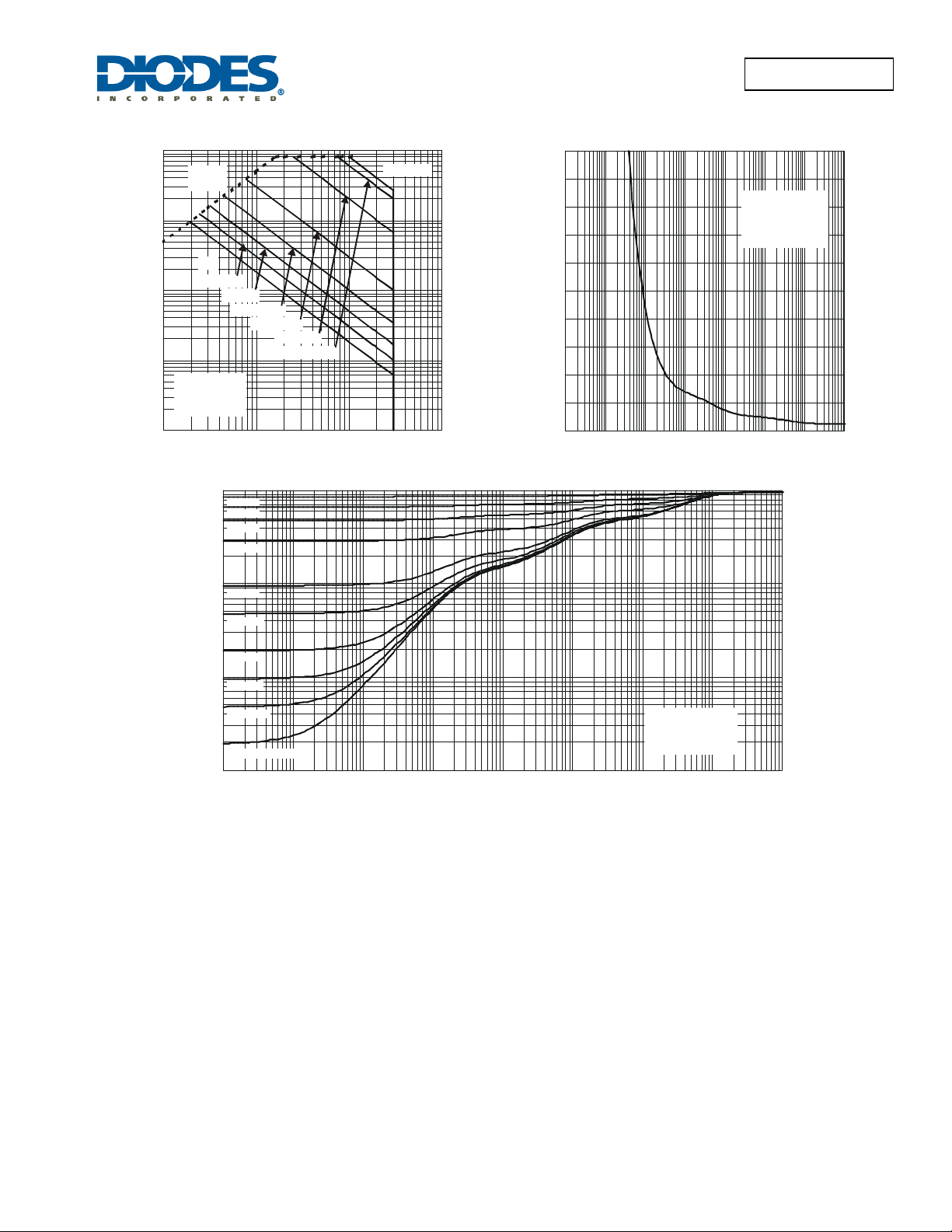
Fig. 1 SOA, Safe Operat ion Area
1
D = 0.9
D = 0.7
E
D = 0.5
D = 0.3
100
100
90
(W)
80
70
IWE
Single Pulse
R = 61C/W
R = r * R
T - T = P * R
60
50
ANSIEN
40
30
EAK
20
(PK)
10
0
0.001 0.01 0.1 1 10 100 1,0000.0001
t1, PULSE DURATION TIME (sec)
Fig. 2 Single Pulse Maximum Power Dissipation
°
θ
JA
θθ
JA(t) (t) JA
JA JA(t)
ESIS
0.1
D = 0.1
MAL
D = 0.05
D = 0.02
0.01
D = 0.01
ANSIEN
D = 0.005
r(t),
D = Single Pulse
0.001
0.00001 0.0001 0.001 0.01 0.1 1 10 100 1,000
R = r * R
θ
JA(t) (t)
R = 60C/W
JA
Duty Cycle, D = t1/t2
θθJA
°
t1, PULSE DURATION TIME (sec)
Fig. 3 Transi ent Thermal Resis t ance
POWERDI is a registered trademark of Diodes Incorporated
DMS3014SFG
Document number: DS35594 Rev. 6 - 2
3 of 8
www.diodes.com
May 2012
© Diodes Incorporated
 Loading...